Abstract
With the rapid development of new energy sources, distributed power supplies are widely used in DC microgrid systems. The DC–DC converter, as the hub for transmitting energy between the distributed power supply and the DC bus, plays an important role in the stability of the whole system performance. Due to the complexity of the actual working environment, the DC bus voltage is often affected by uncertainties such as fluctuations of distributed power supply and random changes in load, so the reliability of DC–DC converters is increasingly required, and it is difficult for traditional linear controllers to ensure that a DC–DC converter operates stably over a wide range. In order to solve this problem, this paper takes the Single-Inductor Triple-Output (SITO) Buck converter, which represents the multi-input and multi-output system, as the research object, analyzes the respective operating characteristics and control difficulties, and proposes Objective Holographic Feedback Nonlinear Control (OHFNC) to improve the stability of the research system. The optimal control based on objective holographic feedback is proposed to address the cross-influence factors between the multiple output branches of the Buck converter and the inability of accurate feedback linearization. Finally, the validity of the model and theoretical analysis is verified by simulation and experimental results.
1. Introduction
The proliferation of highly integrated electronic devices has led to an increase in the number of cell modules and the corresponding design complexity, creating a need for small, cost-effective power sources while facilitating the rapid growth of renewable energy sources [1,2,3,4]. The conventional approach failed to meet these demands until the emergence of Single-Inductor Multiple-Output (SIMO) switching converters, thus offering an effective solution [5,6,7]. SIMO converters aid in reducing device quantities and the overall converter size, thereby enhancing efficiency and lowering costs. Additionally, the separate control of each output branch enables optimized performance [8,9,10]. With the rapid development of new energy sources, distributed power supplies have been widely used in DC microgrid systems. The stability of the DC–DC converter, as the core component for energy transfer between the distributed power supply and the DC bus, is of great significance to ensure the overall system performance. Due to the complexity of the actual operating conditions, the DC bus voltage is often affected by uncertainties such as fluctuations in distributed power sources and random changes in loads. As a result, the reliability of DC–DC converters faces escalating requirements, which makes it difficult for conventional linear controllers to ensure the consistent operation of DC–DC converters over a wide range. The focus of this paper is to address this issue by investigating the CCM SITO buck converter.
The Single-Inductor Multiple-Output (SIMO) switching converter possesses a more intricate topology and represents a typical nonlinear coupled system in contrast to the conventional Single-Input Single-Output switching converter. The output branches of SIMO converters exhibit inductive coupling, where the inductance currents of different output branches are interrelated, resulting in one output branch. The load changes will have an impact on other output branches, which is the cross-influence between output branches. Therefore, a modification in the load of a particular output branch can induce fluctuations in the output voltage of the remaining branches [11,12]. Cross-influence impacts the steady-state voltage accuracy of individual output branches and can potentially jeopardize the system’s stability if it becomes severe [13,14]. Consequently, it is crucial to minimize the crossover effects of SIMO switching converters [15,16]. In response to this issue, the literature has put forth numerous control methods aimed at mitigating the cross-effects of SIMO switching converters. The earliest technique proposed was time-division multiplexing control [17,18]. However, it solely applies to Single-Inductor Dual-Output (SIDO) switching converters operating in discontinuous conduction mode (DCM), resulting in significant current ripple and energy loss. Conversely, the continuous conduction mode (CCM) SIMO converter provides benefits such as reduced voltage and current ripple, as well as enhanced efficiency in comparison to DCM SIMO converters [19,20].
To summarize all control theories and control methods for all DC–DC converters, they can be broadly classified into linear and nonlinear control theories based on the system model. Strictly speaking, nonlinearity is universal, and nonlinear systems are the most general systems and have a wide range of applications in different fields [21,22], while linear systems represent only a special case of nonlinear systems. The linear system structure is relatively simple, and its physical description and mathematical solution are relatively easy to realize; because of this, the linear control theory and research methods have established a perfect theoretical system, and there is a trend of applying linear control theory to study and analyze the DC–DC converter system [23]. However, the DC–DC converter is a nonlinear system that requires linearization to apply linear control methods. A common linear control method is the small-signal analysis method, which linearizes the system by adding a small perturbation near a specific operating point, then neglects the higher-order terms to obtain a linear model and finally applies linear control theory to its design. However, this control method has two limitations: firstly, the linearization is an approximate model near a specific operating point of the system, which can only reflect the local operating state of the system; if it is beyond the range of the operating point, the method is no longer applicable due to the nonlinear characteristics of the higher-order subterms, and therefore it cannot reflect the characteristics of the system in the whole state space. Secondly, the phenomenon of nonlinear systems is much more complex than that of linear systems, and the manifestation is also very different. In addition to the operating state exhibited by linear systems, nonlinear systems also have nonlinear phenomena such as bifurcation, chaos, and self-oscillation [24,25], which cannot be explained by linear control theory.
In order to solve the above problems, classical nonlinear control methods, such as the phase plane method, the input–output stability theory, the describing function method, the Lyapunov method, and so on, were proposed in the early days and applied to the field of power electronic converters and achieved better results. Since the 1980s, due to the rapid development of nonlinear analysis and nonlinear generalized functions in mathematical theory, the newly developed nonlinear control methods have also received more and more attention, including passive control, sliding mode control, adaptive control, robust control, etc. [26,27], and have also achieved certain results in power electronic converters. Although all these nonlinear control methods can keep the DC–DC converter stable, it is difficult for them to balance the steady-state accuracy and dynamic response of the system. In DC microgrids, for some multi-input and multi-output converters, the controller design process will be very complicated.
The study conducted by the authors of [28] proposed the Common-Mode–Differential-Mode (CMDM) Voltage Control for the CCM Single-Inductor Dual-Output (SIDO) switching converter, aiming to enhance the mitigation of crossover effects among the output branches. Nevertheless, the system exhibits slow response characteristics. The researchers in [29] introduced a digital multivariable voltage-based control technique to mitigate the crossover effects of the SIDO converter. However, as the number of output branches increases, the computational complexity of this method grows, resulting in decreased efficiency and increased implementation challenges. The researchers in [30,31,32] proposed a current-type ripple control technique for the CCM SIDO switching converter, demonstrating the effective suppression of crossover effects among the output branches. However, this technique necessitates an additional compensation circuit for each control loop, significantly augmenting the complexity of controller design and leading to higher system losses as the number of output branches grows. Finally, ref. [33] introduced a compensation-network-free voltage-based technique, effectively eliminating the requirement for each control loop to include a compensation network and substantially mitigating the cross-influence across the output branches.
The control methods proposed in the aforementioned literature effectively mitigate the crossover effects between the output branches of the SIMO converter. However, these methods predominantly rely on the small-signal model, which has inherent limitations. The small-signal model is an approximate linear model derived by ignoring higher-order subterms at the system’s equilibrium point. Exact feedback linearization (EFL) is a technique that overcomes these limitations by mapping the original nonlinear system to a linear system while preserving the higher-order nonlinear terms, thus ensuring the integrity of the system [34,35,36]. Reference [37] proposed EFL optimal control for the SIDO Boost converter. The authors redefined the output function satisfying the system’s EFL and designed a control law using optimal control techniques to effectively minimize the crossover effects between the output branches. However, constructing the output function that satisfies EFL involves solving partial differential equations, which can be more complex for higher-order systems and may be infeasible for certain systems [38].
The above literature has applied the exact feedback linearization method in combination with other linear control methods to design respective satisfactory controllers for the system under study. It has also concluded that for a nonlinear system model, if the relative order of the output function of the system to the system is equal to the order of the system, the system can be linearized to a controllable linear system by exact feedback. However, this condition is more demanding for some complex systems and is not easy to satisfy, so the main focus of people’s research has been to reconstruct the output function that can linearize the system with exact feedback. For some systems, although it is not possible to linearize their exact feedback, it is possible to linearize part of their exact feedback, but the remaining part is still nonlinear. At this point, the stability of the nonlinear part also needs to be discussed, and it is common to use system dynamics expansion methods to address the steady-state performance of certain state quantities [39]. In view of the advantages and disadvantages of exact feedback linearization and partially exact feedback linearization, the SITO Buck converter is investigated in this paper.
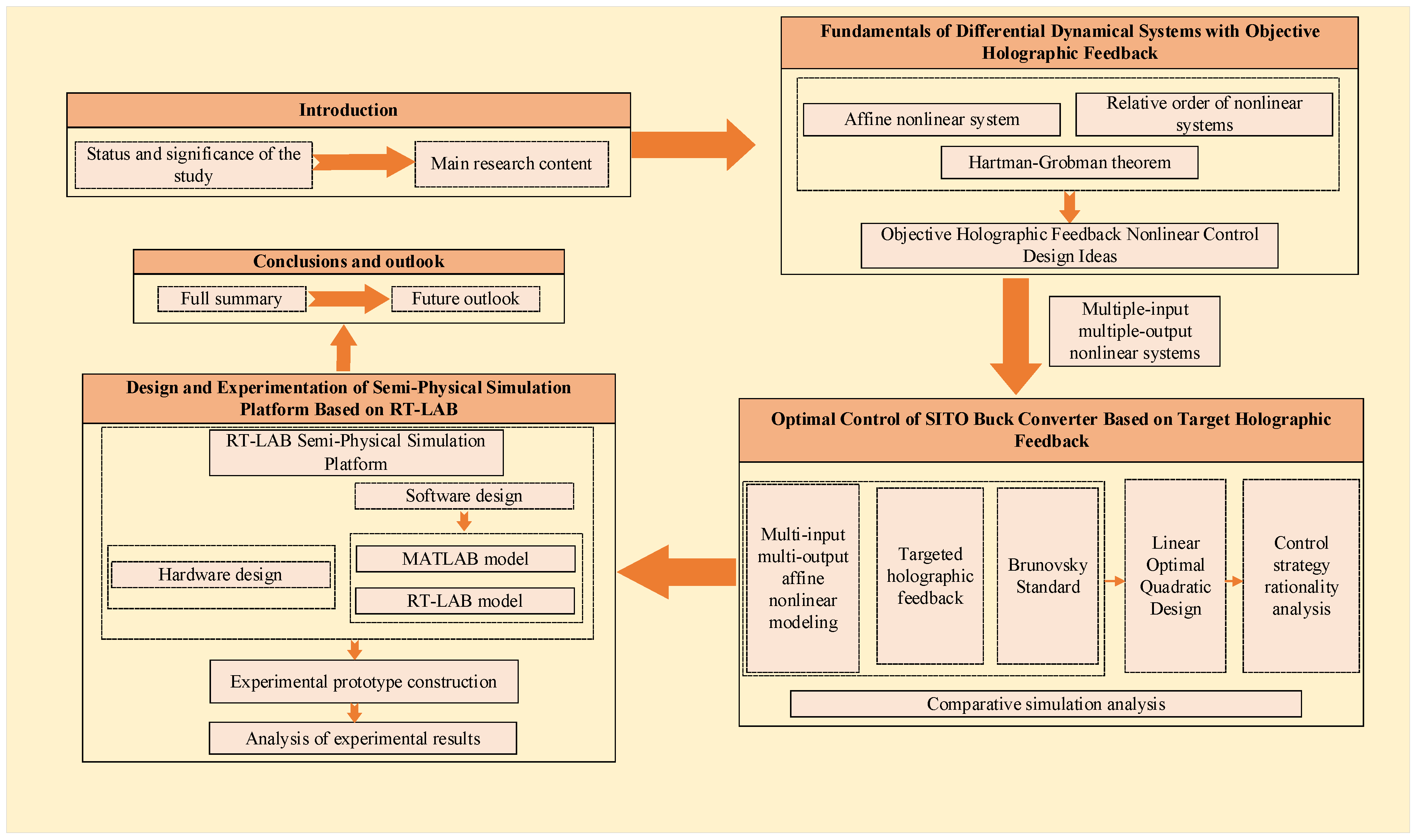
This paper presents the Objective Holographic Feedback Nonlinear Control (OHFNC) method for the controller design of the Current-Controlled Mode Synchronous Inverted Triple-Output (CCM SITO) Buck converter to tackle the shortcomings of exact feedback linearization (EFL) [40]. The OHFNC method eliminates the need for constructing an output function to achieve EFL and only requires the system variables to have first-order relative derivatives. This requirement is easy to satisfy and simplifies the design process. Additionally, the paper uses the Hartman–Grobman theory to elucidate the mechanism of OHFNC’s role in the CCM SITO Buck converter. It is demonstrated that, in the vicinity of the system’s equilibrium point, OHFNC can configure the system by assigning poles near the equilibrium point and independently constrain and control each target variable using nonlinear feedback. In this article, an optimal control strategy based on objective holographic feedback is proposed for a SITO Buck converter, which takes into account both the higher-order terms of the nonlinear system as well as the exact linearization of the system and suppresses the crossover effects between the output branches of a single-inductor multi-output converter. The workflow diagram of the paper is shown below in Figure 1.
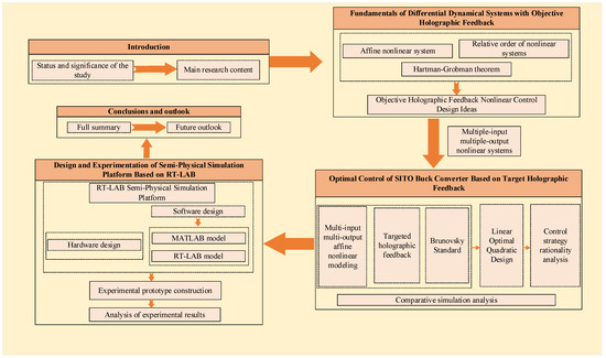
Figure 1.
Paper workflow diagram.
2. Theory of Nonlinear Systems
2.1. Affine Nonlinear System
The mathematical models of the systems studied herein are all affine nonlinear models with differential equations of the following form:
Here, x is the state variable, and are n × m dimensional function vectors, is an m-dimensional output function vector, and is an m-dimensional input (control) vector. When m = 1, the system is a Single-Input Single-Output affine nonlinear system, which is a special case in this form, and the model can be categorized as a Single-Input Single-Output (SISO) system or Multiple-Input Multiple-Output (MIMO) system based on the number of inputs and the number of outputs.
2.2. SIMO System Objective Holographic Feedback Nonlinear Control Idea
For system (1) with m = 1, the system is a Single-Input Single-Output (SISO) affine nonlinear system. This is where most nonlinear control design methods generally deal with the case where the input quantity is equal to the output quantity, or can only deal with nonlinear systems with the same number of inputs and control targets. However, in most of the nonlinear systems, where the (output quantity) target quantity is more than the input quantity, the use of the previous control methods can only ensure that part of the target quantity can be effectively constrained, but it is difficult to ensure that the not-constrained target quantity has good static and dynamic performance. At this point, system (1), with more outputs (target quantities) than inputs, is defined as a Single-Input Multiple-Output (SIMO) affine nonlinear system in the following form:
Here, x is an n-dimensional state variable, f(x) and g(x) are n-dimensional vector fields, u is a control input, and y is an m-dimensional output column vector, i.e., the target quantity of the system.
In general, the output function y defined in system (2) should have good static and dynamic performance according to practical requirements; it can be a state variable or a function of state variables. For system (2), it is not required that the input and output have the same dimension. If, in the output function y, there exists a function component y that has a first-order relative order to system (2), the Single-Input Multiple-Output affine nonlinear system (2) is said to objective holographic feedback. However, the case where the relative order is greater than 1 is avoided because the higher-order components are not easily accessible while the condition of first-order relative order is easily satisfied.
Usually, system (2) is expected to have its output function track in a given state stably after a perturbation; in other words, the desired state of y is given in advance. Assuming that is the reference trajectory that the output function wishes to track, the following multi-objective equation is obtained:
Here, Ii is the tracking deviation of the target quantity.
For nonlinear system (2), the control task is to design a nonlinear control law that ensures that (2) remains stable after a perturbation and that the target quantity still tracks its reference trajectory stably while the multi-objective Equation (3) satisfies the following relationship:
It is clear that when Equation (4) is satisfied, the problem of the accurate tracking of each target quantity is effectively solved. For nonlinear system (2), satisfying the objective holographic feedback is easily satisfied, i.e., there exists an output function ym of relative order 1 for the system, and the following relation is obtained [41]:
Equation (5) plays an important role in closely linking the target quantities of the system to the input control quantities.
The tracking deviation equation in (3) is actively constructed as a system of dynamic equations and is required to conform to the Brunovsky standard type of order m as follows:
Expanding Equation (6) and combining it with Equation (5) yields the following:
Here, v is the control law of linear system (6), whereby the control law of the original nonlinear system can be expressed thus:
It is worth noting that system (6) is a fully controllable linear system, which can be analyzed according to the knowledge of linear control theory, and the optimal control theory, sliding mode control, and other methods can be used to design the feedback control law v of system (6), and ultimately the feedback control law u of the original nonlinear system (2) can be obtained.
3. CCM SITO Buck Converter
3.1. Operating States and Switching Timings
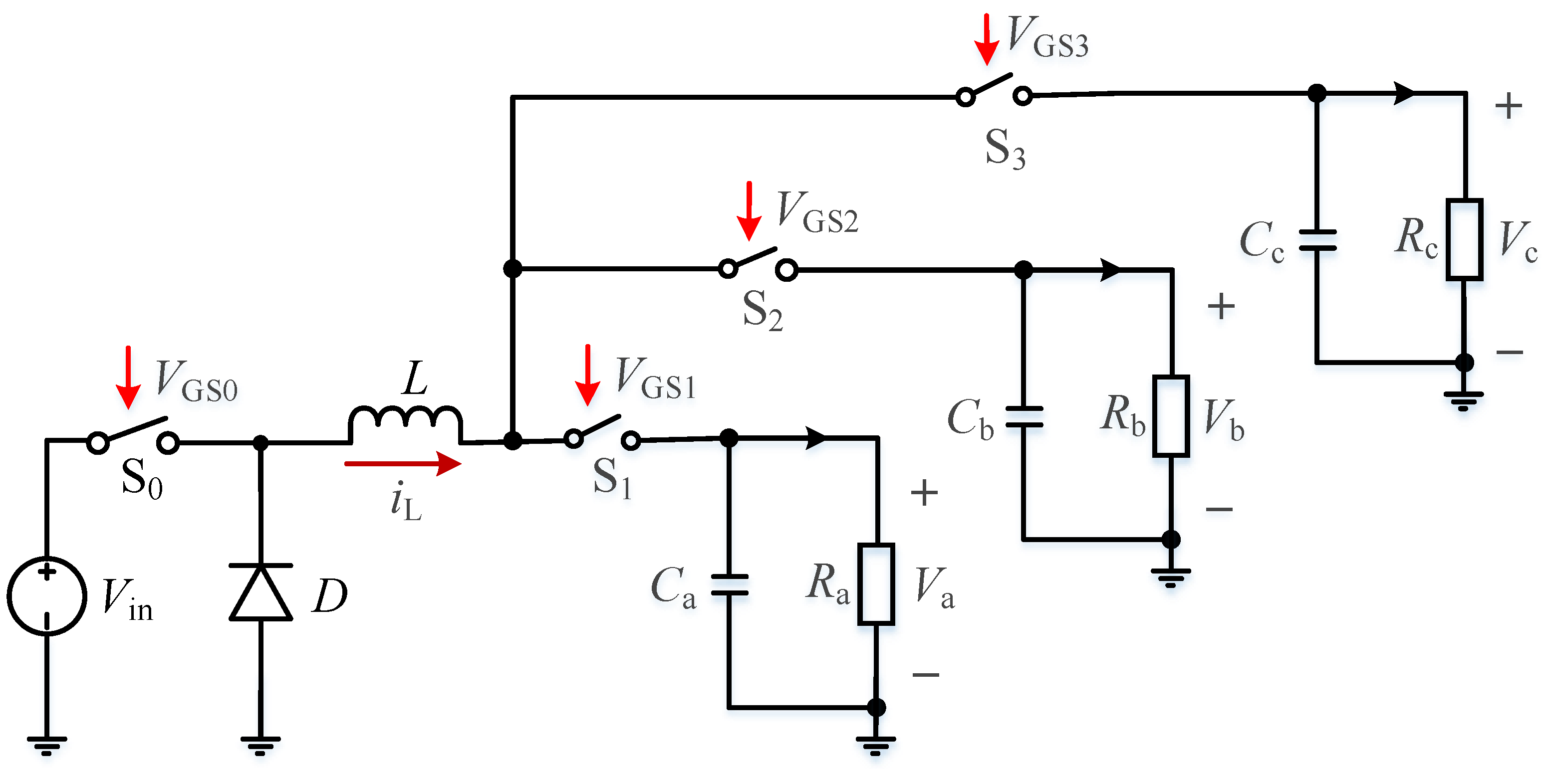
Figure 2 shows the main circuit diagram of the SITO Buck converter. The circuit includes an input voltage source, denoted as Vin; a filter inductor, denoted as L; branch switching tubes labeled as S1, S2, and S3; the main switching tube, denoted as S0; the diode, denoted as D; output filter capacitors, labeled as Ca, Cb, and Cc; and load resistors denoted as Ra, Rb, and Rc. The main switching tube S0 and the diode D control the energy transfer from the input voltage source Vin. The output branches Vgs0–Vgs3 are responsible for driving the switches S0–S3. The corresponding switch on-duty ratios are denoted as D0, D1, D2 and D3, respectively. When the SITO Buck converter operates in continuous conduction mode, the sum of D1, D2, and D3 is equal to 1, indicating complementary control pulses of the switch tubes in the three output branches.
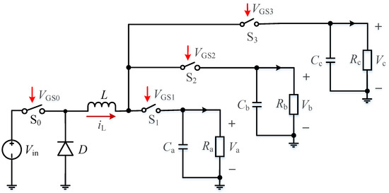
Figure 2.
Main circuit diagram of SITO Buck converter.
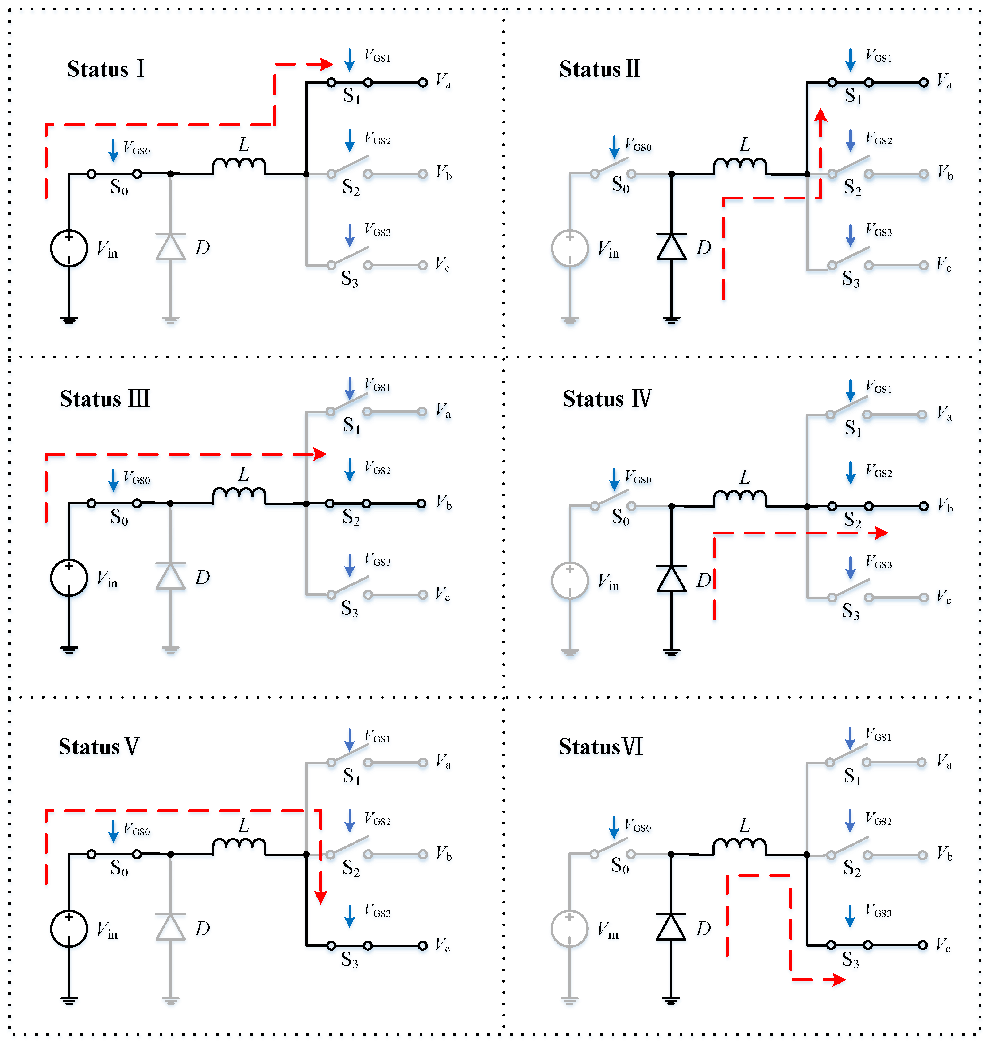
The operating states of the continuous conduction mode (CCM) SITO Buck converter can be divided into six types according to the on-time sequence of the main and output branch switch tubes, as shown in Figure 3.
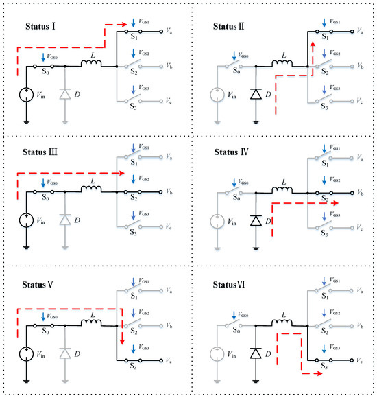
Figure 3.
Operating state of CCM SITO Buck converter.
- State I: Switching tubes S0 and S1 are on; S2, S3, and D are off; the input voltage Vin charges the inductor L and capacitor Ca while supplying power to the load Ra; and the inductor current rises linearly through the output branch a with a slope m1 = (Vin − Va)/L.
- State II: Diode D and switching tube S1 are on; S0, S2 and S3 are off; at this time, the energy stored in inductor L discharges capacitor Ca and load Ra; the inductor current changes through the output branch a with a slope −m2 = −Vin/L.
- State III: Switching tubes S0 and S2 are on; S1, S3, and D are off; the input voltage Vin charges the inductor L and capacitor Cb while supplying power to the load Rb; and the inductor current rises linearly through the output branch a with a slope m3 = (Vin − Vb)/L.
- State IV: Diode D and switching tube S2 are on; S0, S1, and S3 are off; at this time, the energy stored in inductor L discharges capacitor Cb and load Rb; the inductor current changes through the output branch a with a slope −m4 = −Vb/L.
- State V: Switching tubes S0 and S3 are on; S1, S2, and D are off; the input voltage Vin charges the inductor L and capacitor Cc while supplying power to the load Rc; and the inductor current rises linearly through the output branch a with a slope m5 = (Vin − Vc)/L.
- State VI: Diode D and switch tube S3 conduct; S0, S1, and S2 are off; inductor L discharges to capacitor Cc and load Rc; the inductor current through the output branch c with a slope −m6 = −Vc/L linearly decreases; and after a period of time, the system returns to the initial value, and the whole process is repeated from state I.
The analysis illustrates that when either the input voltage or the rectifying diode charges one output branch, the output capacitors of the remaining two output branches continue to operate simultaneously to discharge the associated loads.
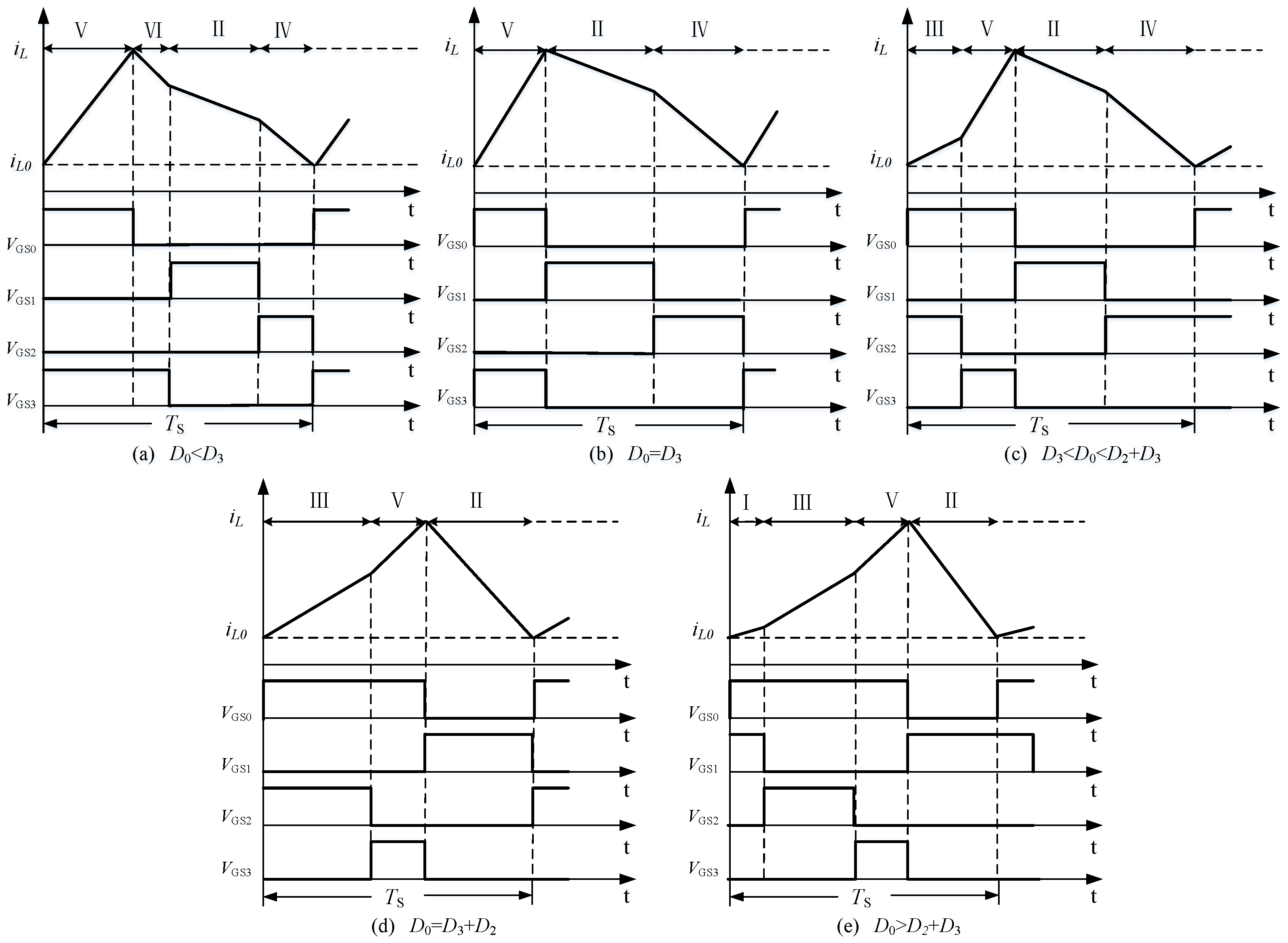
3.2. CCM SITO Buck Converter Switching Timing
Based on the relative duty cycle relationship between the primary switching tube (S0) and the auxiliary switching tube (S3), the operational timing of the CCM SITO Buck converter is categorized as five modes during a single switching cycle. These modes include (a) D0 < D3, (b) D0 = D3, (c) D3 < D0 < D2 + D3, (d) D0 = D2 + D3, and (e) D0 > D2 + D3, as depicted in Figure 4.
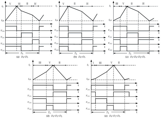
Figure 4.
Switching timing diagrams of the CCM SITO Buck converter.
In the case where the CCM SITO Buck converter operates with a timing of D0 < D3, its operational sequence progresses as follows: state V→state II→state IV→state VI. During this sequence, the inductor undergoes one charging state followed by three discharging states while exhibiting a pattern of “rise–fall–fall–fall” for the steady-state inductor current. Figure 4a depicts both the steady-state inductor current as well as the operational timing of this converter.
When the CCM SITO Buck converter works in the timing D0 = D3, resulting in the following sequence: state V→state II→state IV. In this process, the inductor experiences one charging state and two discharging states, and the steady-state inductor current exhibits a “rise-fall-fall” pattern. Refer to Figure 4b for the steady-state inductor current and operating timing of the converter.
When the CCM SITO Buck converter works in timing D3 < D0 < D2 + D3, its working process is state III→state V→state II→state IV. The inductor functions in two charging states and two discharging states during this process, and the steady-state inductor current exhibits a pattern. Refer to Figure 4c for the steady-state inductor current and working timing of the converter.
When the CCM SITO Buck converter works in the timing D0 = D2 + D3, its working process is state III→state V→state II. During this process, the inductor undergoes two charging states and one discharging state, and the steady-state inductor current exhibits a pattern of “rising–rising–falling”. The steady-state inductor current and the timing of the converter’s operation are depicted in Figure 4d.
When the CCM SITO Buck converter works in timing D0 > D2 + D3, its working process is state I→state III→state V→state II. The inductor goes through three charging states and one discharging state in this process, and the steady-state inductor current exhibits a trend of “rising–rising–rising–declining”. The steady-state inductor current and the timing of the converter’s operation are depicted in Figure 4e.
3.3. Output Branch Steady-State DC Voltage Gain
When the CCM SITO Buck converter operates in a stable manner within one switching cycle, the following relationship is derived based on the volt-second balance principle of the inductor [33].
The average inductor current in the system and the load current in each output branch adhere to the following relationship:
The following relationships are valid: Ia = Va/Ra, Ib = Vb/Rb, Ic = Vc/Rc. The equation satisfies D3 = 1 − D1 − D2.
The average current in the inductance conforms to the following relationship:
Hence, the DC voltage gain expression for each load in the output branches can be derived from Equations (9)–(11) as follows.
Similarly, the duty cycle of the primary switching transistor and the switching transistors in each output branch can be calculated as follows.
Equation (13) demonstrates the relationship between the branch output voltage gain of the CCM SITO Buck converter and the on–off duty cycle of both the primary switching transistor and the switching transistors in the output branches. Furthermore, Equation (13) illustrates that the output voltage gain of each branch depends not only on its own load but also on the loads of the other branches. Hence, when the loads of the other branches vary, the output voltage value of each respective branch will change due to the cross-influence among the output branches.
4. CCM SITO Buck Converter Model and Control Design
4.1. CCM SITO Buck Converter Affine Nonlinear Model
This paper focuses on studying the operation of the CCM SITO Buck converter within a single cycle, specifically during the timing condition D3 < D0 < D2 + D3, which corresponds to the steady-state operation shown in Figure 4c. Based on Figure 3, the state equations corresponding to four switch states, namely II, IV, III, and V, are derived [42].
Here, t1, t2, and t3 represent the durations of operation for switching states II, IV, and III, respectively. The coefficient matrix of the state variables, denoted as x = [x1, x2, x3, x4]T = [i1, va, vb, vc]T, can be obtained through computational analysis.
Thus, the unified model of the CCM SITO Buck converter can be described as
Here, u0 = 0.1; ua = 0.1; ub = 0.1; uc = 0.1; when taken as 0, it indicates the off state of the switching tubes S0, S1, S2, and S3; when taken as 1, it indicates the on state of the corresponding switching tubes and satisfies uc = 1 − ub − ua.
The converter can be modeled using the state-space averaging method based on the state-space averaging modeling principle, which applies when the switching frequency of the CCM SITO Buck converter circuit significantly exceeds the system’s characteristic frequency. The fourth-order state-space averaging model of the converter is obtained by substituting the on-duty ratios d0, d1, d2, and d3 of the switching tubes S0, S1, S2, and S3 into Equation (15) in place of u0, ua, ub, and uc.
Let represent the average value of the system’s state variables. By defining the input vector , we can derive the mean state equation of the CCM SITO Buck converter, which can be expressed as
Let us consider the multi-input affine nonlinear control system presented below:
This fits in the following equation:
Hence, the CCM SITO Buck converter should be regarded as a nonlinear coupled system with multiple inputs and outputs.
4.2. Design of Objective Holographic Feedback Nonlinear Control Method for CCM SITO Buck Converter
In the case of the CCM SITO Buck converter, the output function (10) of the system is commonly represented as y1 = h1(x) = x2 − varef, y2 = h2(x) = x3 − vbref, and y3 = h3(x) = x4 − vcref. Here, varef, vbref, and vcref correspond to the reference values for the output voltage of each output branch. Consequently, the calculation proceeds as follows.
Assuming there is a scalar function h(x) and a vector field f(x), the dot product of the derivative of function h(x) and vector field f(x) is called the Lie derivative of function h(x) along vector field f(x), denoted as .
By analogy, the high-order Lie derivative of function h(x) with respect to vector field f(x) can be obtained:
At the same time, the Lie derivative of function with respect to other vector fields g(x) can also be obtained:
The relative order of the system can be calculated as follows, defining the relative order discriminant matrix:
Here, r1, r2, and r3 are the relative orders of the output functions y1, y2, and y3 to the system. The values of each element of the relative order discriminant matrix are calculated:
And the relative order of each element of to the system can be obtained as r1 = r2 = r3 = 1. so the following matrix is derived:
The relative order of the system can be obtained as , which is lower than the order of the system, 4. In this case, the system is not perfectly linearized into a completely controllable linear system. Nevertheless, the system can be linearized using objective holographic feedback. While operating the CCM SITO Buck converter, our main concern lies in the static and dynamic performance of the inductor current and each output voltage. Therefore, we redefine the output function vector as while represents the reference objective that the output function vector aims to track. This redefinition allows us to obtain the following multi-objective equation.
In the given context, Ii represents the tracking error of the output variable. It is our expectation that the nonlinear feedback control law designed for this system guarantees system stability even in the presence of disturbances. Additionally, we aim to ensure that each target quantity exhibits excellent performance while ensuring that the multi-objective system of Equation (25) satisfies the following relationship.
Equation (26) inherently addresses the tracking problem for all target quantities of the system. Upon the satisfaction of the condition in Equation (26), each chosen target quantity can effectively track its reference value, enabling effective and accurate tracking for each target quantity. We actively employ the multi-objective deviation Equation (25) to construct a linear system that adheres to the 4th order Brunovsky standard type in the following manner.
Here, the virtual control vector is , and when the selected output function is the inductor current iL and the three output circuits are va, vb, and vc, they all have a first-order relative order to the system, and the following relationship is obtained.
The virtual control vector, denoted as V, can be derived using optimal control design theory by choosing specific performance metrics from the following set.
The linear feedback control quantity can then be obtained as
By combining Equations (28) and (30), the nonlinear control law for the CCM SITO Buck converter system can be obtained by solving the following equation.
4.3. Analysis of Objective Holographic Feedback Nonlinear Control Principle for CCM SITO Buck Converter
This section provides a theoretical derivation to explain the underlying reason why OHFNC effectively addresses the stability problem of the CCM SITO Buck converter in a Multiple-Input Multiple-Output system and elucidates the nature of its solution to the multi-target control equation. Utilizing the Hartman–Grobman theorem, the deduction of OHFNC’s role in the CCM SITO Buck converter is explained, specifically its ability to accurately track the output function to its reference trajectory and ensure the satisfactory dynamic and static performance of the target quantities. At this stage, system (10) is derived by disregarding the higher-order terms at the hyperbolic equilibrium point , employing a Taylor series expansion, resulting in the following primary approximation system.
Here,
Here, d0e, d1e, and d2e represent the steady-state values of duty cycles d0, d1, and d2, respectively. Similarly, x1e, x2e, x3e, and x4e represent the steady-state values of the inductor current iL and output voltages va, vb, and vc, respectively. Assume xor and yor represent the reference trajectories of the previously approximated system (32). For these assumed reference trajectories, there will always be input vectors uor that allow xor, yor, and uor to satisfy system (32). This assumption ensures that xor and yor, along with the input vector uor, can cause xo and yo to converge to xor and xor. Now, we select the linear non-singular matrix Tm and perform the linear transformation xs = Tmxo and ys = Tmyo to convert system (32) into the Luenberger controlled standard type, resulting in the following.
Based on this assumption, there also exist linear transformations xsr = Tmxor and ysr = Tmyor that satisfy system (33), resulting in the following reference system.
To design the control law for the linearized system (34), we can utilize the objective holographic feedback control. This involves selecting three output quantities, namely iL, vb and vc, from the system, which has a first-order relative order. We will relabel these output quantities as . As a result, we obtain the following.
Similarly, in the context of Equation (35), the reference trajectory for variable , denoted as , must satisfy the following relationship.
Utilizing the previously proposed objective holographic nonlinear control strategy, we can formulate the integrated control law as follows, represented by Equation (33).
In the equation , and ,, , and .
We substitute the primary linear control law, approximated from Equation (37), into Equation (33) and subtract Equation (34). Finally, we combine the result with Equation (36) to obtain the following.
Equation (38) can be further simplified as follows.
This yields the following equation:
From the control theory of linear systems, it is known that a feasible solution to Equation (40), i.e., , must be chosen to ensure that there is a feedback coefficient corresponding to it, and the appropriate value can be chosen to configure the poles of the system. The system described by Equation (39) represents a tracking error equation based on the output vector and shares the same dimensions as the original system (33). They are equivalent to each other. When the system described by Equation (39) is stable, it not only solves the stability problem of the original system but also effectively constrains each target quantity xs, causing them to converge towards their respective reference trajectory xsr. Equation (37) is further rewritten as
This applies in the following equation:
From Equation (41), it can be seen that after selecting the appropriate feedback coefficients , the original system can be used directly in the original system without transforming it into the Luenberger standard type. Based on the aforementioned discussion, it can be concluded that OHFNC is actually used to ensure the good dynamic and static performance of each target quantity by selecting the appropriate feedback coefficients to configure the poles of the SITO Buck converter system in the field of equilibrium points and to constrain each target quantity.
5. Simulation Experimental Results and Analysis of CCM SITO Buck Converter
5.1. Numerical Simulation Analysis
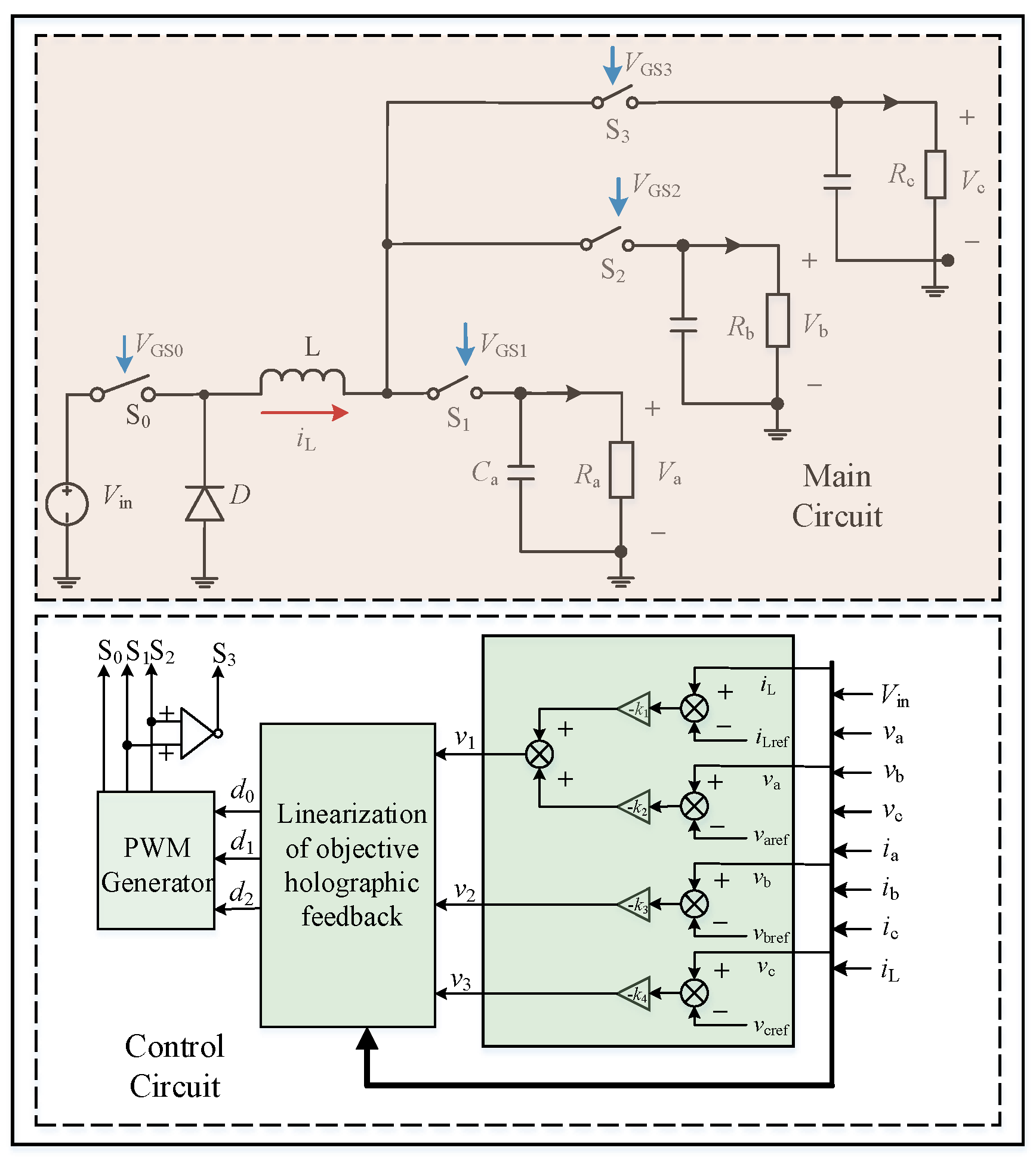
In order to further validate the correctness and effectiveness of the OHFNC method, this paper presents a simulation model of the CCM SITO Buck converter with a resistive load. The simulation is conducted using the MATLAB/Simulink simulation platform. Figure 5 is a Block diagram of the closed-loop control of a CCM SITO Buck converter. The simulation parameters are provided in Table 1. Equation (5) is utilized to verify the accurate timing of the CCM SITO Buck converter based on the data in Table 1, demonstrating that D3 < D0 < D1 + D2. Furthermore, an analytical comparison between OHFNC and common-mode–differential-mode voltage control is performed to showcase the superiority of OHFNC. Equation (19) is employed to determine the feedback coefficients k1 = 80,000, k2 = 80,000, k3 = 80,000, and k4 = 96,000 based on the feedback parameters. Additionally, the poles of the closed-loop system (10) in its equilibrium field are configured as s1 = −810, s2 = −6370, s3 = −43,900 + 29,200i, and s4 = −43,900 − 29,200i. The simulation results are then used to validate these parameters and illustrate that OHFNC is more effective in suppressing crossover effects between the output branches while enhancing the responsiveness and robustness of the CCM SITO Buck converter compared to common-mode–differential-mode voltage control [43]. Overall, these simulation results confirm the effectiveness and practicality of OHFNC as a control method for power electronics applications.
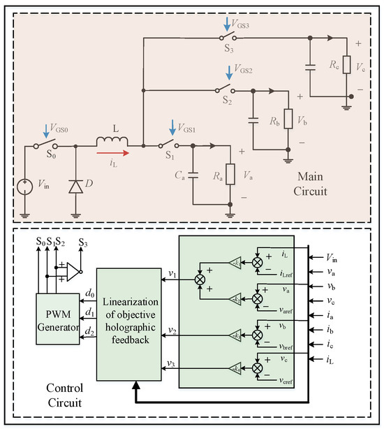
Figure 5.
Block diagram of closed-loop control of CCM SITO Buck converter.

Table 1.
System parameters of the CCM SITO Buck converter.
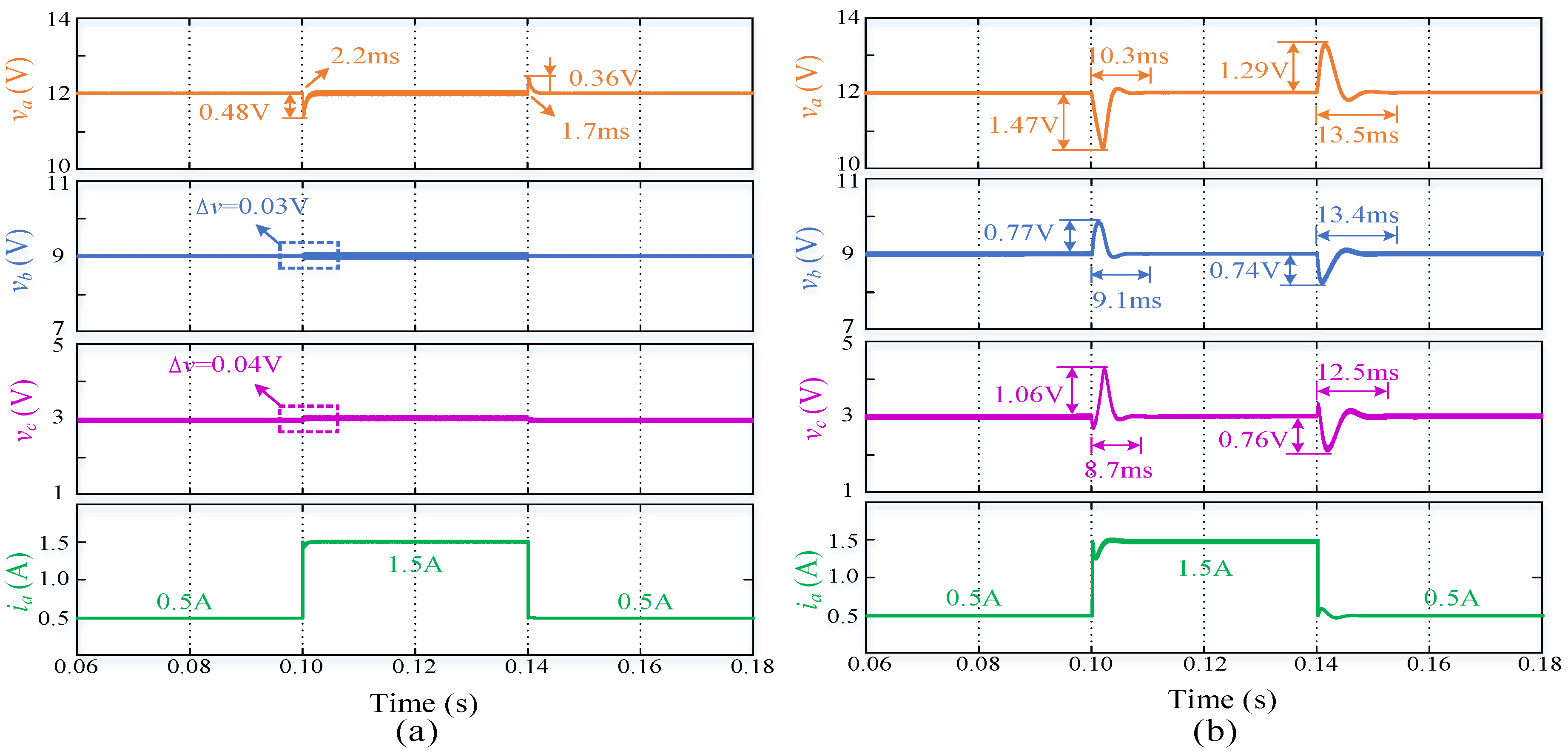
Figure 6 illustrates the system’s response waveform when the load in branch a undergoes a sudden change, specifically when the current ia jumps from 0.5 A to 1.5 A and then returns to 0.5 A. Simulation results demonstrate that both control strategies can successfully eliminate static errors in each output parameter. However, they exhibit distinct advantages and disadvantages in the dynamic process. During the transition from 0.5 A to 1.5 A in ia, the voltage va in branch a experiences a maximum change of 0.48 V under the OHFNC method but swiftly returns to its steady-state value within 2.2 ms. In contrast, the changes in vb and vc are significantly smaller, with values of only 0.03 V and 0.04 V, respectively. These values suggest that the impact of output branch a on branches b and c is negligible. Alternatively, when utilizing the common-mode–differential-mode voltage control strategy, the maximum change in va reaches 1.47 V before returning to its steady-state value within 10.3 ms. Similarly, the changes in vb and vc amount to 0.77 V and 1.06 V, respectively, before returning to their steady-state values in 9.1 ms and 8.7 ms, respectively. Consequently, in this instance, the cross-influences of branch a on branches b and c amount to 0.77 V and 1.06 V, respectively. Conversely, when ia jumps back from 1.5 A to 0.5 A, the OHFNC-controlled system experiences a maximum change of 0.36 V in the a-way voltage va, which subsequently recovers to the steady-state value within 1.7 ms. Likewise, the maximum changes in vb and vc remain identical to the previous values. In contrast, the system under the common-mode–differential-mode voltage control strategy exhibits a maximum variation of 1.29 V in va, which returns to the steady-state value after 13.5 ms. Similarly, vb and vc experience maximum variations of 0.74 V and 0.76 V, respectively, which also return to their steady-state values after 13.4 ms and 12.5 ms, respectively. Consequently, the cross-influences of branch a on output branches b and c are 0.74 V and 0.76 V, respectively. Overall, the simulation results demonstrate that OHFNC effectively reduces the cross-influence among the output branches while improving the system’s response speed when compared to the common-mode–differential-mode voltage control.
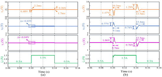
Figure 6.
Dynamic response waveform of the system when Ra jumps: (a) Objective Holographic Feedback Nonlinear Control; (b) common-mode–differential-mode voltage control.
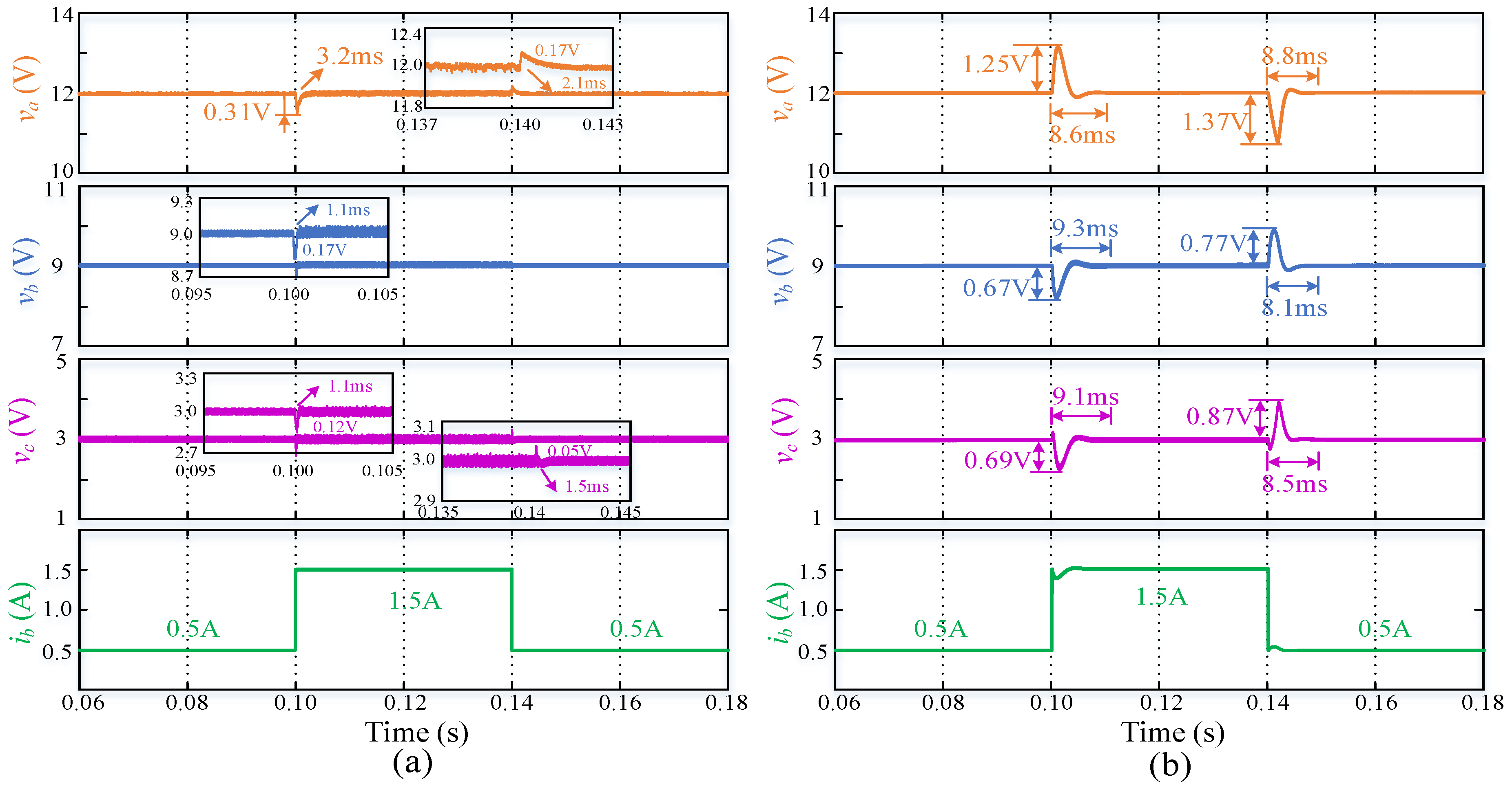
In Figure 7, the response waveform of the system is shown when the load in branch b jumps, i.e., when the current ib jumps from 0.5 A to 1.5 A and then jumps back to 0.5 A. From the simulation results, it can be observed that when ib jumps from 0.5 A to 1.5 A, the maximum voltage changes in the three output voltages of the output branches are 0.31 V, 0.17 V, and 0.12 V under OHFNC, and they return to the steady-state values after 3.2 ms, 1.1 ms, and 1.1 ms, respectively. Conversely, when employing the common-mode–differential-mode voltage control, the three output voltages experience maximum changes of 1.25 V, 0.67 V, and 0.69 V. The voltages then return to their steady-state values after respective durations of 8.6 ms, 8.1 ms, and 8.5 ms. When ib jumps back from 1.5 A to 0.5 A, the output voltages va, vb, and vc require durations of 2.1 ms, 1.1 ms, and 1.5 ms, respectively, to return to the steady state under OHFNC. The corresponding maximum sudden changes are 0.17 V, 0.02 V, and 0.05 V, respectively.
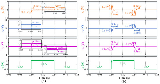
Figure 7.
Dynamic response waveform of the system when Rb jumps: (a) Objective Holographic Feedback Nonlinear Control; (b) common-mode–differential-mode voltage control.
In contrast, when employing the common-mode–differential-mode voltage control strategy, it takes 8.8 ms, 8.1 ms, and 8.5 ms for the output voltages va, vb, and vc to return to the steady-state value. The corresponding maximum voltage changes are 1.37 V, 0.77 V, and 0.87 V. Overall, the simulation results illustrate that OHFNC enables the output voltage to return to the steady-state value more swiftly in the presence of sudden load changes. Additionally, it effectively mitigates the cross-influence on other output branches. OHFNC exhibits commendable self-regulation and significantly enhances the system’s responsiveness and robustness compared to the common-mode–differential-mode voltage control approach.
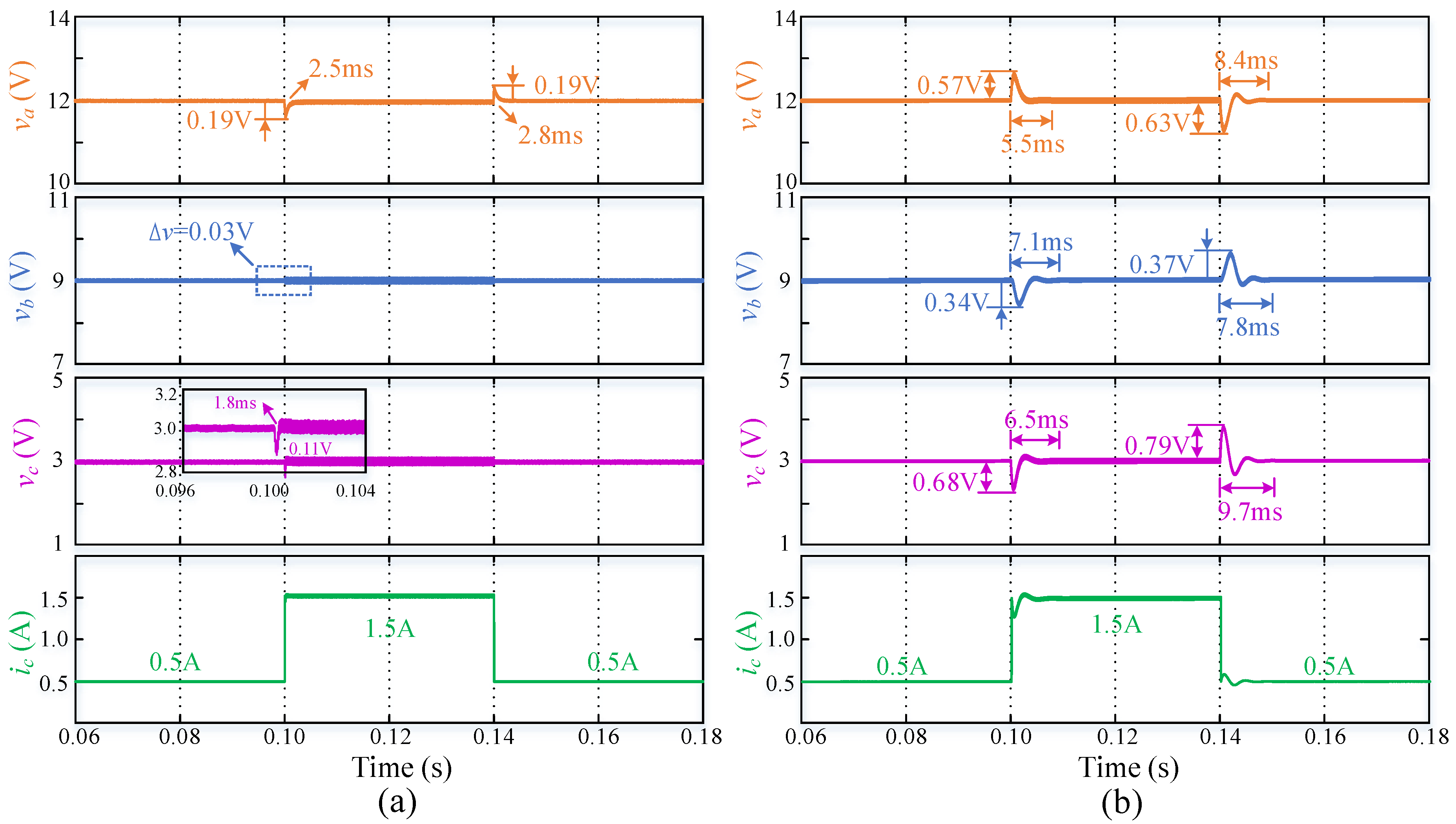
The response waveform of the system during a load jump in branch c is depicted in Figure 8. The waveform reveals that when ic jumps from 0.5 A to 1.5 A, the output voltages va, vb and vc undergo maximum voltage changes of 0.19 V, 0.03 V, and 0.11 V, respectively, under OHFNC. These voltages return to their steady-state values after 2.5 ms, 1.2 ms, and 1.8 ms, respectively. Conversely, when the common-mode–differential-mode voltage control is employed, the maximum voltage variations in va, vb, and vc are 0.57 V, 0.34 V, and 0.68 V, respectively, and it takes 5.5 ms, 7.1 ms, and 6.5 ms, respectively, for them to return to their steady-state values. During the reverse jump of the c-way output current ic from 1.5 A to 0.5 A, the output voltages va, vb, and vc experience maximum voltage changes of 0.19 V, 0.04 V, and 0.05 V, respectively, under OHFNC. Moreover, the recovery times are significantly shorter at 2.8 ms, 1.3 ms, and 1.6 ms, respectively. In contrast, the system output voltages va, vb, and vc require considerably longer durations of 8.4 ms, 7.8 ms, and 9.7 ms, respectively, to regain their stable voltage states when employing the common-mode–differential-mode voltage control strategy. These extended durations correspond to output voltage burst values of 0.63 V, 0.37 V, and 0.79 V, respectively. Overall, the simulation results demonstrate that OHFNC effectively mitigates the cross-influence between output branches, exhibiting superior self-regulation and faster response speed when compared to common-mode–differential-mode voltage control. The simulation results provide a verification of OHFNC’s efficacy as a control method for power electronics applications.
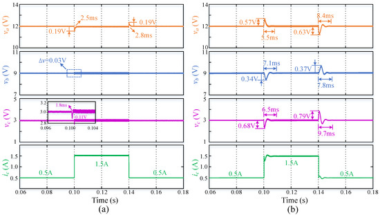
Figure 8.
Dynamic response waveform of the system when Rc jumps: (a) Objective Holographic Feedback Nonlinear Control; (b) common-mode–differential-mode voltage control.
In conclusion, during abrupt changes in the load on one output branch, the output voltage undergoes a single-pole change under OHFNC. Conversely, the response of the output voltage displays an oscillatory process when subjected to the common-mode–differential-mode voltage control method. This method hinders the normal operation of the CCM SITO Buck converter. Therefore, the proposed OHFNC method surpasses the common-mode–differential-mode voltage control method. Table 2 displays the comparative results of the system simulation for convenient analysis.
Table 2.
Comparison of OHFNC and common-mode–differential-mode voltage control simulation results.
5.2. Comparison of Performance Results with Existing Literature
The comparison of simulated experimental waveforms illustrated above highlights the superiority of the OHFNC strategy. Additionally, to further demonstrate the effectiveness of OHFNC in mitigating the cross-effect among output voltages and to offer a more intuitive representation of the cross-effect’s magnitude, a cross-influence factor, denoted as FOM (cross), is defined according to the literature [44]. The formula for calculating FOM (cross) is as follows.
Let δvi (i = a, b, c) denote the maximum change value of each output voltage when there is an abrupt change in the output branch load. Also, Vi (i = a, b, c) represents the DC steady-state value of each branch output voltage. δii (i = a, b, c) refers to the amount of change in output load current when there is an abrupt change in the output branch load. Lastly, Ii represents the DC steady-state value of the output branch load.
By combining the simulated waveforms of the system when the load jumps in the output branch as shown in Figure 5, Figure 6 and Figure 7, and according to Equation (21), the output dynamic performance of the CCM SITO Buck converter under the effect of the Objective Holographic Feedback Nonlinear Control can be obtained. At this point, we only analyze the dynamic process corresponding to the load current jump from 0.5 A to 1.5 A, as shown in Table 3.
Table 3.
Dynamic performance of the CCM SITO Buck converter under OHFNC.
To highlight the superiority of OHFNC, we assess the performance of the CCM SITO Buck converter with OHFNC in comparison to the existing literature on Single-Input Dual-Output (SIDO) converters. As shown in Table 4, it is evident that our proposed CCM SITO Buck converter system with OHFNC exhibits a maximum cross-effect coefficient of 0.02 and the maximum value of during load variations, indicating superior cross-effect suppression.
Table 4.
Comparison with existing literature on SIMO switching converters.
6. Physical Verification
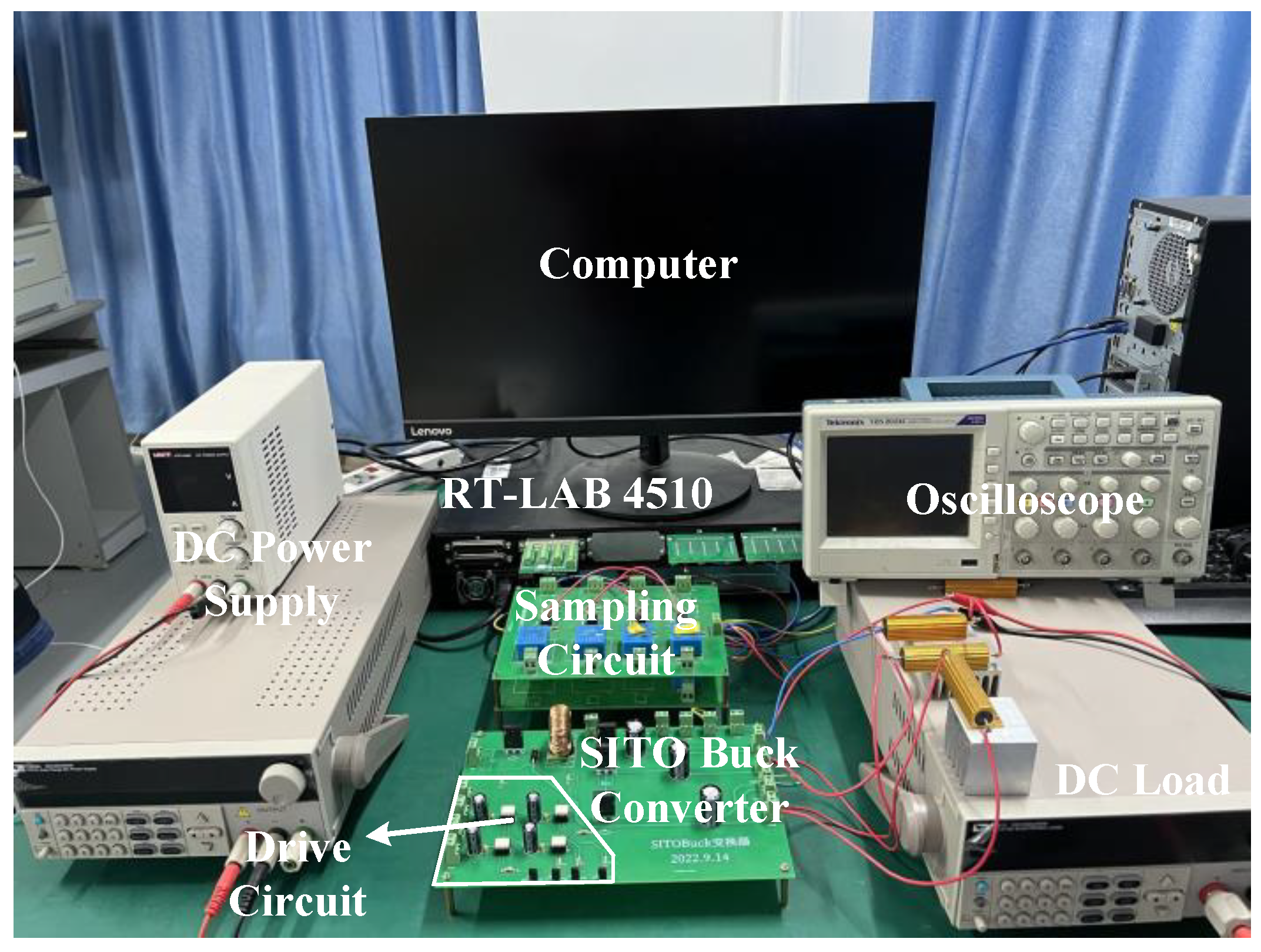
To validate the feasibility of OHFNC, we developed a principle prototype of a SITO Buck converter for conducting semi-physical simulation experiments. The RT-LAB OP4510 controller (Shanghai Keliang Information Technology Co., Ltd., Shanghai, China) was utilized, and the experimental parameters were set to be identical to the simulation parameters. The prototype setup consisted of a GW PSB-1400M (GW instek, Suzhou, China) direct current (DC) power supply, an Airtex IT8812 DC electronic load (Guangzhou Junda Instrument Co., Ltd., Guangzhou, China), sampling circuitry, driving circuitry, and a Tektronix TSD 2024C (Tech Technology Co., Ltd., Shanghai, China) digital storage oscilloscope with four channels. Figure 9 depicts the test prototype.

Figure 9.
Semi-physical simulation platform of CCM SITO Buck converter based on RT-LAB OP4510.
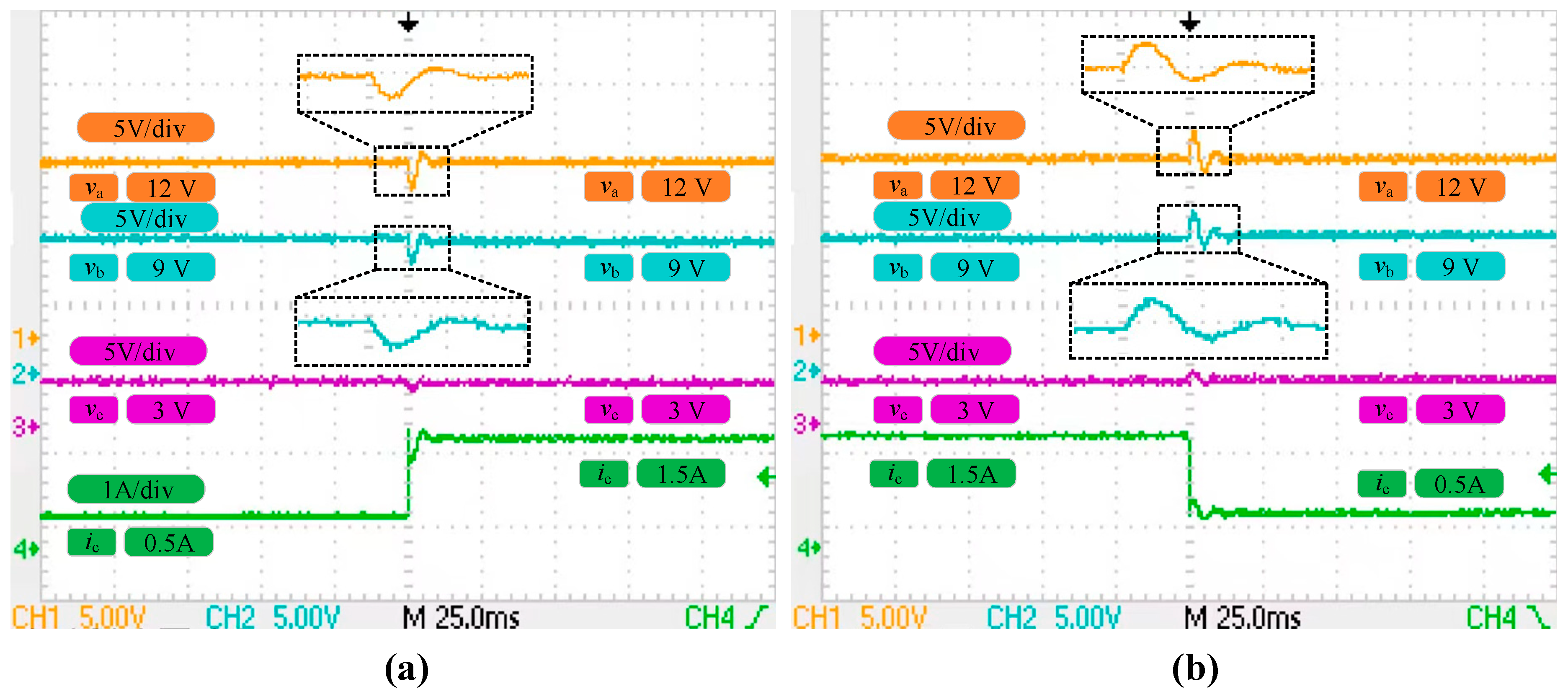
Figure 10 displays the experimental response curves of the three output branches of the system in response to a load perturbation in branch a. From Figure 10a, it is observed that the voltages va, vb, and vc recovered to their steady-state values after a brief disturbance, despite the current ia jumping from 0.5 A to 1.5 A. Specifically, the voltages va, vb, and vc returned to their steady-state values within 5 ms, 5 ms, and 3 ms, respectively, accompanied by maximum voltage changes of 0.9 V, 0.6 V, and 0.2 V. This suggests minimal cross-influences of branch a on branches b and c. Figure 10b demonstrates that following a brief disturbance, the output voltages va, vb, and vc return to steady states when the current ia jumps from 1.5 A to 0.5 A. The voltages va, vb, and vc returned to their steady-state values within 6 ms, 6 ms, and 4 ms, respectively, with maximum voltage changes of 0.8 V, 0.7 V, and 0.3 V. Therefore, we can conclude that the cross-influence of branch a on branch b is 0.7 V, and on branch c, it is 0.3 V.
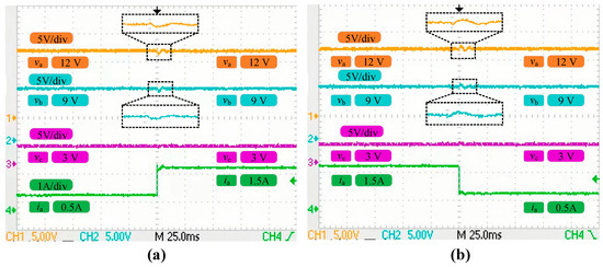
Figure 10.
Dynamic response waveform of the system during the ia jump. (a) Experimental waveform when ia jumps from 0.5 A to 1.5 A. (b) Experimental waveform when ia jumps from 1.5 A to 0.5 A.
Figure 11 showcases the experimental response waveforms of the system during a sudden load change in output branch b. As visible in Figure 11a, when the load current ib jumped from 0.5 A to 1.5 A, which corresponded to a reduction in resistive load from 18 Ω to 6 Ω, va, vb, and vc required 5 ms, 5 ms, and 3 ms, respectively, to recover to the new steady state. During this time, the three output branches displayed overshoot voltages of 0.6 V, 0.8 V, and 0.1 V, respectively. Subsequently, Figure 11b shows that upon reducing the load current ib from 1.5 A to 0.5 A,va, vb, and vc took 8 ms, 8 ms, and 3 ms, respectively, to return to the steady-state values before and after the load jump. During this period, the three output branches displayed overshoot voltages of 1 V, 0.8 V, and 0.2 V, respectively. Based on these waveforms, it is evident that the crossover effect on the output branch c is negligible during abrupt changes in the load current ib.
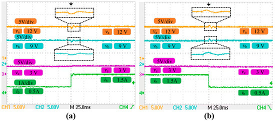
Figure 11.
Dynamic response waveform of the system during ib jump. (a) Experimental waveform when ib jumps from 0.5 A to 1.5 A. (b) Experimental waveform when ib jumps from 1.5 A to 0.5 A.
Figure 12 displays the experimental response waveforms of the system when there is a sudden change in the load for output branch c. In Figure 12a, when the load current ic increase from 0.5 A to 1.5 A (which corresponds to a decrease in resistive load from 6 Ω to 2 Ω), va, vb, and vc take 8 ms, 8 ms, and 4 ms, respectively, to return to the steady-state before the load jump, and reach the new reference voltage level. During this period, the three output branches exhibit overshoot voltages of 2 V, 2 V, and 0.9 V, respectively. Furthermore, in Figure 12b, when the load current ic decreases from 1.5 A to 0.5 A, va, vb, and vc take 8 ms, 9 ms, and 5 ms, respectively, to return to the steady state. Additionally, during this process, the three output branches show overshoot voltages of 1.8 V, 1.5 V, and 0.8 V, respectively. The analysis suggests that the most significant crossover effect occurs on the a branch when there is a load jump in output branch c. Moreover, output branch c is well regulated and exhibits minimal voltage changes.
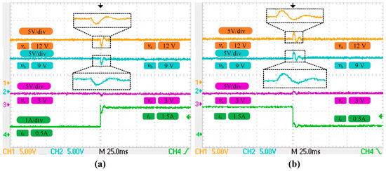
Figure 12.
Dynamic response waveform of the system during ic jump. (a) Experimental waveform when ic jumps from 0.5 A to 1.5 A. (b) Experimental waveform when ic jumps from 1.5 A to 0.5 A.
Table 5 lists all the experimental results. Generally, when a sudden change in load takes place in any of the output branches, the voltage of each branch can quickly return to its steady-state value. There is also a slight overshoot voltage observed in all branches. The experimental waveforms align with the results obtained from numerical simulations, providing additional evidence of the effectiveness of OHFNC.
Table 5.
Experimental results data of SITO Buck converter.
7. Conclusions and Future Perspectives
The paper has presented the OHFNC method devised to mitigate crossover effects among the output branches of the CCM SITO Buck converter. It has examined the converter’s operational states and switching timings, consequently deriving the associated switching conditions. Utilizing the equation of state, the paper has established an affine nonlinear model for the converter wherein the inductor current and output voltages are chosen as the output functions. These functions, along with their respective reference values, form the deviation equation system. Employing the affine nonlinear model, a fourth-order linear system of the Brunovsky standard-type has been constructed, and a control law has been designed using the optimal quadratic form to achieve the complete decoupling of the system. The connection between the control law and the target quantity has been established based on the conditions of objective holographic feedback. By applying the Hartman–Grobman theorem, the paper has mathematically deduced that OHFNC effectively enforces constraints and controls the target quantity by configuring the poles of the system through appropriate feedback coefficients, thereby driving the state variables to converge towards their respective reference trajectories. Simulation results have demonstrated that OHFNC surpasses common-mode–differential-mode voltage control in suppressing crossover effects while simultaneously enhancing system responsiveness and robustness. Experimental results have further validated the practicality and effectiveness of OHFNC. In conclusion, OHFNC has proven to be an effective control approach for the CCM SITO Buck converter, offering the potential to reduce crossover effects among output branches in power electronics applications.
The OHFNC method applied in this paper has been developed based on the affine nonlinear model, on which future studies can further consider the effects of nonlinear factors such as core saturation, inductor resistance, and other factors. By establishing a more accurate nonlinear model and combining it with advanced control methods, the steady-state performance and response speed of the system can be effectively improved. Meanwhile, with the continuous popularization and development of artificial intelligence technologies, future research can try to introduce these technologies into the OHFNC method. For example, deep learning algorithms can be used to model and optimize the system to achieve more accurate and adaptive control strategies. Meanwhile, combining algorithms such as reinforcement learning can further improve the robustness and adaptability of the system. Finally, this paper has focused on the single-inductor multi-output Buck converter, and future research can consider the cross-influence problem in the case of more complex topologies, such as multi-inductors and multi-outputs. This will provide more comprehensive and practical solutions for a wider range of scenarios in power electronics applications.
Author Contributions
Conceptualization, supervision, writing—review and editing, J.L.; methodology, software, writing—original draft preparation, H.D.; validation, investigation, P.C.; project administration, P.Z. All authors have read and agreed to the published version of the manuscript.
Funding
This research was funded by the National Natural Science Foundation of China Project no. 61863003.
Data Availability Statement
The original contributions presented in this study are included in the article. Further inquiries can be directed to the corresponding author.
Acknowledgments
Thank you to all the individuals who have contributed to this research.
Conflicts of Interest
The authors declare that they have no known competing financial interests or personal relationships that could have appeared to influence the work reported in this paper.
References
- Chen, G.; Liu, Y.; Ma, M.; Hu, Y.; Qing, X. An independently controlled magnetic coupling multi-output buck converter with mixed modes for unbalanced loads. IEEE Trans. Ind. Inform. 2020, 16, 7499–7509. [Google Scholar] [CrossRef]
- Markkassery, S.; Saradagi, A.; Mahindrakar, A.D.; Lakshminarasamma, N.; Pasumarthy, R. Modeling, design and control of non-isolated single-input multi-output zeta–buck–boost converter. IEEE Trans. Ind. Appl. 2020, 56, 3904–3918. [Google Scholar]
- Mahjoub, S.; Labdai, S.; Chrifi-Alaoui, L.; Drid, S.; Derbel, N. Design and implementation of a Fuzzy logic supervisory based on SMC controller for a Dual Input-Single Output converter. Int. J. Electr. Power Energy Syst. 2023, 150, 109053. [Google Scholar] [CrossRef]
- Sambaiah, K.S.; Jayabarathi, T. Optimal Modeling and Allocation of Mixed Wind and Solar Generation Systems in Electric Distribution Networks. IETE J. Res. 2022, 68, 4129–4141. [Google Scholar] [CrossRef]
- Chen, G.; Liu, Y.; Qing, X.; Ma, M.; Lin, Z. Principle and topology derivation of single-inductor multi-input multi-output DC–DC converters. IEEE Trans. Ind. Electron. 2021, 68, 25–36. [Google Scholar] [CrossRef]
- Hosseini, A.; Badeli, A.S.; Davari, M.; Sheikhaei, S.; Gharehpetian, G.B. A Novel, Software-Defined Control Method Using Sparsely Activated Microcontroller for Low-Power, Multiple-Input, Single-Inductor, Multiple-Output DC–DC Converters to Increase Efficiency. IEEE Trans. Ind. Electron. 2023, 70, 2959–2970. [Google Scholar] [CrossRef]
- Liu, W.; Zhang, H.; Zhang, X.; Liu, W. Dynamical Analysis of Hybrid-Scale Bifurcation in One-Cycle Controlled Single-Inductor Dual-Output Buck DC–DC Converters. Int. J. Bifurc. Chaos 2023, 33, 2350004. [Google Scholar] [CrossRef]
- Patra, P.; Patra, A.; Misra, N. A single-inductor multiple-output switcher with simultaneous buck, boost, and inverted outputs. IEEE Trans. Power Electron. 2012, 27, 1936–1951. [Google Scholar] [CrossRef]
- Huang, W.; Qahouq, J.A.A.; Dang, Z. CCM–DCM power-multiplexed control scheme for single-inductor multiple-output DC–DC power converter with no cross regulation. IEEE Trans. Ind. Appl. 2017, 53, 1219–1231. [Google Scholar] [CrossRef]
- Goh, T.Y.; Ng, W.T. Single discharge control for single-inductor multiple-output DC–DC buck converters. IEEE Trans. Power Electron. 2018, 33, 2307–2316. [Google Scholar] [CrossRef]
- Wang, Y.; Xu, J.; Zhou, G. A cross regulation analysis for single-inductor dual-output CCM buck converters. J. Power Electron. 2016, 16, 1802–1812. [Google Scholar] [CrossRef]
- Jin, W.; Lee, A.T.L.; Tan, S.C.; Hui, S.R. Single-inductor multiple-output inverter with precise and independent output voltage regulation. IEEE Trans. Power Electron. 2020, 35, 11222–11234. [Google Scholar] [CrossRef]
- Nayak, G.; Nath, S. Decoupled voltage-mode control of coupled inductor single-input dual-output buck converter. IEEE Trans. Ind. Appl. 2020, 56, 4040–4050. [Google Scholar] [CrossRef]
- Zheng, Y.; Guo, J.; Leung, K.N. A single-inductor multiple-output buck/boost DC–DC converter with duty-cycle and control-current predictor. IEEE Trans. Power Electron. 2020, 35, 12022–12039. [Google Scholar] [CrossRef]
- Chen, H.; Huang, C.J.; Kuo, C.C.; Lin, L.-C.; Ma, Y.-S.; Yang, W.-H.; Chen, K.-H.; Lin, Y.-H.; Lin, S.-R.; Tsai, T.-Y. A single-inductor dual-output converter with the stacked MOSFET driving technique for low quiescent current and cross regulation. IEEE Trans. Power Electron. 2019, 34, 2758–2770. [Google Scholar] [CrossRef]
- Li, X.L.; Dong, Z.; Chi, K.T.; Lu, D.D.C. Single-inductor multi-input multi-output DC–DC converter with high flexibility and simple control. IEEE Trans. Power Electron. 2020, 35, 13104–13114. [Google Scholar] [CrossRef]
- Ma, D.; Ki, W.H.; Tsui, C.Y.; Mok, P. Single-inductor multiple-output switching converters with time-multiplexing control in discontinuous conduction mode. IEEE J. Solid-State Circuits 2003, 38, 89–100. [Google Scholar]
- Ma, D.; Ki, W.H.; Tsui, C.Y. A pseudo-CCM/DCM SIMO switching converter with freewheel switching. IEEE J. Solid-State Circuits 2003, 38, 1007–1014. [Google Scholar]
- Wang, Y.; Xu, J.; Qin, F.; Mou, D. A capacitor current and capacitor voltage ripple controlled SIDO CCM buck converter with wide load range and reduced cross regulation. IEEE Trans. Ind. Electron. 2022, 69, 270–281. [Google Scholar] [CrossRef]
- Nayak, G.; Nath, S. Unified model of peak current mode controlled coupled SIDO converters. IEEE Trans. Ind. Electron. 2021, 69, 11156–11164. [Google Scholar] [CrossRef]
- Din, A.F.U.; Mir, I.; Gul, F.; Akhtar, S. Development of reinforced learning based non-linear controller for unmanned aerial vehicle. J. Ambient. Intell. Hum. Comput. 2023, 14, 4005–4022. [Google Scholar] [CrossRef]
- Taimoor, M.; Aijun, L.; Samiuddin, M. Sliding mode learning algorithm based adaptive neural observer strategy for fault estimation, detection and neural controller of an aircraft. J. Ambient. Intell. Hum. Comput. 2021, 12, 2547–2571. [Google Scholar] [CrossRef]
- Duan, G. Theory of Linear Systems; Science Press: Beijing, China, 2016. [Google Scholar]
- Wang, Y.; Xu, L.; Li, A.; Liao, K. Dynamic behavior analysis of current-type controlled single inductor dual output Buck converter. Chin. J. Electr. Eng. 2017, 37, 643–652. [Google Scholar]
- Zheng, L.; Lu, S. Control method for fast timescale bifurcation of Boost PFC converter. Power Autom. Equip. 2013, 33, 68–73. [Google Scholar]
- Lascu, C. Sliding-mode direct-voltage control of voltage-source converters with LC filters for pulsed power loads. IEEE Trans. Ind. Electron. 2021, 68, 11642–11650. [Google Scholar] [CrossRef]
- Wai, R.J.; Chen, M.W.; Liu, Y.K. Design of adaptive control and fuzzy neural network control for single-stage boost inverter. IEEE Trans. Ind. Electron. 2015, 62, 5434–5445. [Google Scholar] [CrossRef]
- Trevisan, D.; Mattavelli, P.; Tenti, P. Digital control of single-inductor multiple-output step-down DC–DC converters in CCM. IEEE Trans. Ind. Electron. 2008, 55, 3476–3483. [Google Scholar] [CrossRef]
- Dasika, J.D.; Bahrani, B.; Saeedifard, M.; Karimi, A.; Rufer, A. Multivariable control of single-inductor dual-output buck converters. IEEE Trans. Power Electron. 2014, 29, 2061–2070. [Google Scholar] [CrossRef]
- Wang, Y.; Xu, J.; Yin, G. Cross-regulation suppression and stability analysis of capacitor current ripple controlled SIDO CCM buck converter. IEEE Trans. Ind. Electron. 2019, 66, 1770–1780. [Google Scholar] [CrossRef]
- Zhou, S.; Zhou, G.; Liu, G.; Mao, G. Small-signal modeling and cross-regulation suppressing for current-mode controlled single-inductor dual-output DC–DC converters. IEEE Trans. Ind. Electron. 2021, 68, 5744–5755. [Google Scholar] [CrossRef]
- Patra, P.; Ghosh, J.; Patra, A. Control scheme for reduced cross-regulation in single-inductor multiple-output DC–DC converters. IEEE Trans. Ind. Electron. 2013, 60, 5095–5104. [Google Scholar] [CrossRef]
- Zhou, S.; Zhou, G.; He, M.; Liu, X. The Voltage-mode-ripple Variable Frequency Control for Single-inductor Triple-output Switching Converter. Proc. CSEE 2021, 41, 6003–6013. [Google Scholar]
- Judewicz, M.G.; González, S.A.; Gelos, E.M.; Fischer, J.R.; Carrica, D.O. Exact Feedback Linearization Control of Three-Level Boost Converters. IEEE Trans. Ind. Electron. 2023, 70, 1916–1926. [Google Scholar] [CrossRef]
- Mahmud, M.A.; Roy, T.K.; Saha, S.; Haque, M.E.; Pota, H.R. Robust nonlinear adaptive feedback linearizing decentralized controller design for islanded DC microgrids. IEEE Trans. Ind. Appl. 2019, 55, 5343–5352. [Google Scholar] [CrossRef]
- Chen, C.; Ye, Z.; Huang, J.; Yu, Y.; Xia, Y.; Gao, J. Affine nonlinear control of a multivariate inductive power transfer system with exact linearization. IEEE Trans. Power Electron. 2020, 35, 12728–12740. [Google Scholar] [CrossRef]
- Wu, J.; Lu, Y. Exact feedback linearisation optimal control for single-inductor dual-output boost converter. IET Power Electron. 2020, 13, 2293–2301. [Google Scholar] [CrossRef]
- Li, J.; Zhou, P.; Pan, H.; Feng, D.; Liu, B. Reduced-order controller design for Cuk converters based on objective holographic feedback. J. Power Electron. 2023, 23, 181–190. [Google Scholar] [CrossRef]
- Li, X.; Chen, D.; Liu, S. Multi-objective feedback nonlinear control method for multi-input multi-output differential-algebraic systems. Chin. J. Electr. Eng. 2020, 40, 1465–1474. [Google Scholar]
- Li, J.; Pan, H.; Long, X.; Liu, B. Objective holographic feedbacks linearization control for boost converter with constant power load. Int. J. Electr. Power Energy Syst. 2022, 134, 107310. [Google Scholar] [CrossRef]
- Li, J.; Chen, P.; Zhou, P. Sliding-mode variational structure study of Cuk converter based on target holographic feedback. Int. J. Circ. Theor. Appl. 2024, 52, 1–20. [Google Scholar] [CrossRef]
- Nayak, G.; Nath, S. Small Signal Modeling and Analysis of Single Input Three Output Buck Converter Using Coupled Inductor. In Proceedings of the 2019 National Power Electronics Conference (NPEC), Tiruchirappalli, India, 13–15 December 2019; pp. 1–6. [Google Scholar] [CrossRef]
- Xie, F. Research on Common Mode-Differential Mode Control Single Inductor Dual Output Buck Converter. Master’s Thesis, Shaanxi University of Science and Technology, Xi’an, China, 2021. [Google Scholar] [CrossRef]
- Wang, B.; Xian, L.; Kanamarlapudi, V.R.K.; Tseng, K.J.; Ukil, A.; Gooi, H.B. A digital method of power-sharing and cross-regulation suppression for single-inductor multiple-input multiple-output DC–DC converter. IEEE Trans. Ind. Electron. 2017, 64, 2836–2847. [Google Scholar] [CrossRef]


Disclaimer/Publisher’s Note: The statements, opinions and data contained in all publications are solely those of the individual author(s) and contributor(s) and not of MDPI and/or the editor(s). MDPI and/or the editor(s) disclaim responsibility for any injury to people or property resulting from any ideas, methods, instructions or products referred to in the content. |
© 2025 by the authors. Licensee MDPI, Basel, Switzerland. This article is an open access article distributed under the terms and conditions of the Creative Commons Attribution (CC BY) license (https://creativecommons.org/licenses/by/4.0/).