Article

A Dual-Mode Clock Enhancement Technology N-Path Notch Filter with High Linearity

School of Integrated Circuits, Huazhong University of Science and Technology, Wuhan 430074, China
*
Author to whom correspondence should be addressed.
Electronics 2025, 14(5), 1008; https://doi.org/10.3390/electronics14051008
Submission received: 23 January 2025 / Revised: 22 February 2025 / Accepted: 1 March 2025 / Published: 3 March 2025

Abstract

:
This paper presents a dual-mode clock-enhanced N-path notch filter that offers high linearity. In Mode 1, the clock swing boost mode, the boost module extends the clock swing from VDD to 2 × VDD, thereby significantly improving the filter’s linearity and blocker capacity. In Mode 2, the clock bootstrap mode, the bootstrap module raises the input large signal to the clock on-gate drive voltage, enhancing the large-signal performance. The flexible switching between clock operating modes allows for efficient adaptation to different input conditions and enables optimal clock power consumption. Post-layout simulations conducted using 130-nm SOI CMOS technology demonstrate a tuning range of 0.1 to 1.0 GHz, with a 10.5 dBm blocker 1-dB compression point (B1dB) in boost mode, consuming power between 25.3 and 40.7 mW. In bootstrap mode, the filter achieves a 12.7 dBm B1dB and a 10.1 dBm 1-dB compression point (P1dB), along with an IIP3 of up to 23.9 dBm, while consuming between 35.1 and 55.7 mW.

1. Introduction

In the era of Industry 4.0, wireless communication technology plays an indispensable and crucial role in advancing intelligent production and facilitating the digital transformation of society. As a core technological enabler, wireless communication is extensively applied across a variety of sectors, including mobile communications [1,2,3,4], the Internet of Things (IoT) [5,6,7,8], aerospace, satellite communications for telecommunication, and global positioning systems [9,10,11,12]. The increasing demand for spectrum utilization places greater pressure on the performance of broadband receivers.
In a wideband RF receiving system, two primary interference threats to the system are strong out-of-passband interference and strong in-passband interference. Strong transmitter (TX) leakage can cause saturation of the Low Noise Amplifier (LNA) at the receiver’s (RX) front end, potentially leading to failure of the receiving system [13,14]. To address these challenges, wideband RF filters play a crucial role in significantly improving the performance and stability of the receiver system. Wideband bandpass filters effectively attenuate interfering signals outside the passband, thereby improving the isolation between the receiving and transmitting channels and enhancing the dynamic range and sensitivity of the transceiver system [15].
To enhance transceiver integration, on-chip integratable filter techniques were investigated, including Q-enhanced filters, Gm-C filters, and N-path filters. The Q-enhanced filters are limited by the low Q of the on-chip inductor, which restricts the dynamic range of the filter [16]. Gm-C filters utilize active inductors in place of on-chip inductors, but this results in higher chip power consumption and additional noise, while still failing to achieve a satisfactory dynamic range. Conventional LC notch filters are typically designed with varactor diodes, where the bandwidth is usually defined as a relative bandwidth. While these filters offer high linearity, they fail to provide precise trap frequencies and exhibit insufficient selectivity. Additionally, the on-chip integration area tends to be large. Q-enhanced notch filters and Gm-C notch filters offer advantages in terms of suppression depth and compactness, but they face challenges in tunability, linearity, and power consumption [17,18]. Recently, N-path filters have garnered significant attention due to their broadband capabilities and high-quality factor characteristics. However, numerous challenges remain in improving the linearity and receiver signal-to-noise ratio (SNR) of N-path filters.
The N-path filter is a switched capacitor (SC)-based filter that takes advantage of the combination of switched arrays and capacitors. The basic circuit structure of an N-path filter is shown in Figure 1. The filter consists of an array of N identical switched capacitors, with the center frequency determined by the clock period TS; the N-path clock is a periodic square wave signal, and the duty cycle of the single-path clock is TS/N. The filter operates on the principle of N linear time-invariant (LTI) networks and 2N clock-driven switched passive mixers [19].
The N-path filters offer a promising solution for designing broadband, multiband transceiver front-end systems without the need for SAW filters. However, the linearity of N-path filters is fundamentally limited by their switched capacitor (SC) circuits [20,21]. As the input signal amplitude increases, significant nonlinear effects emerge in the N-path filters, which can degrade the receiver sensitivity or even interfere with the transceiver system function.
To address these issues, researchers have proposed an innovative design based on the N-path filter to improve the linearity of the transmitter leakage suppression band-stop filter. Existing N-path filter linearity enhancement schemes can generally be categorized into two types: bottom-plate mixing with implicit capacitor stacking techniques [22,23] and clock-swing enhancement techniques [24]. Despite the improvements achieved through the bottom-plate mixing technique or implicit capacitors, the switching nonlinear effects remain inevitable when handling large-signal RF inputs. The clock-swing enhancement techniques directly increase the clock swing amplitude, which is intrinsically limited by the transistor source-drain breakdown voltage, leading to a proportional increase in power consumption. There are other papers that propose improvements in terms of filter structure; by connecting the N-path bandpass filter (BPF) in series with the band-reject filter (BRF), the two filters allow independent tuning and are capable of attenuating transmitter leakage of +10 dBm [25]. This approach effectively improves the TX leakage blocking linearity but limits the frequency band and bandwidth of the receiving channel, and its proposed filter is used with narrowband receiving applications, which are not applicable to future ultra-wideband receiving systems.
This work proposed a dual-mode clock-enhanced, high-linearity N-path notch filter. The clock core module is designed with low voltage to reduce power consumption. Mode 1 is the clock swing enhance module. The first level shifter module raises the output of the clock core module to VDD, and the second clock boost circuit enhances the clock swing to a maximum of 2VDD. Mode 2 is the clock bootstrap module. Adding the bootstrap circuit to Mode 1 boosts the clock swing to a maximum of 2VDD + RFIN.
(1)
Mode 1 clock boost: improved linearity and large operating bandwidth with no additional power consumption.
(2)
Mode 2 clock boost + bootstrap: dramatically improves small-signal performance and boosts blocking power capacity, sacrificing power consumption and operating bandwidth.
This paper is organized as follows: Section 2 presents the general structure of the linearity enhancement filter and the clock circuit’s implementation. Section 3 reports and discusses the simulation results of the filters simulated in 130-nm SOI CMOS. Finally, Section 4 concludes.

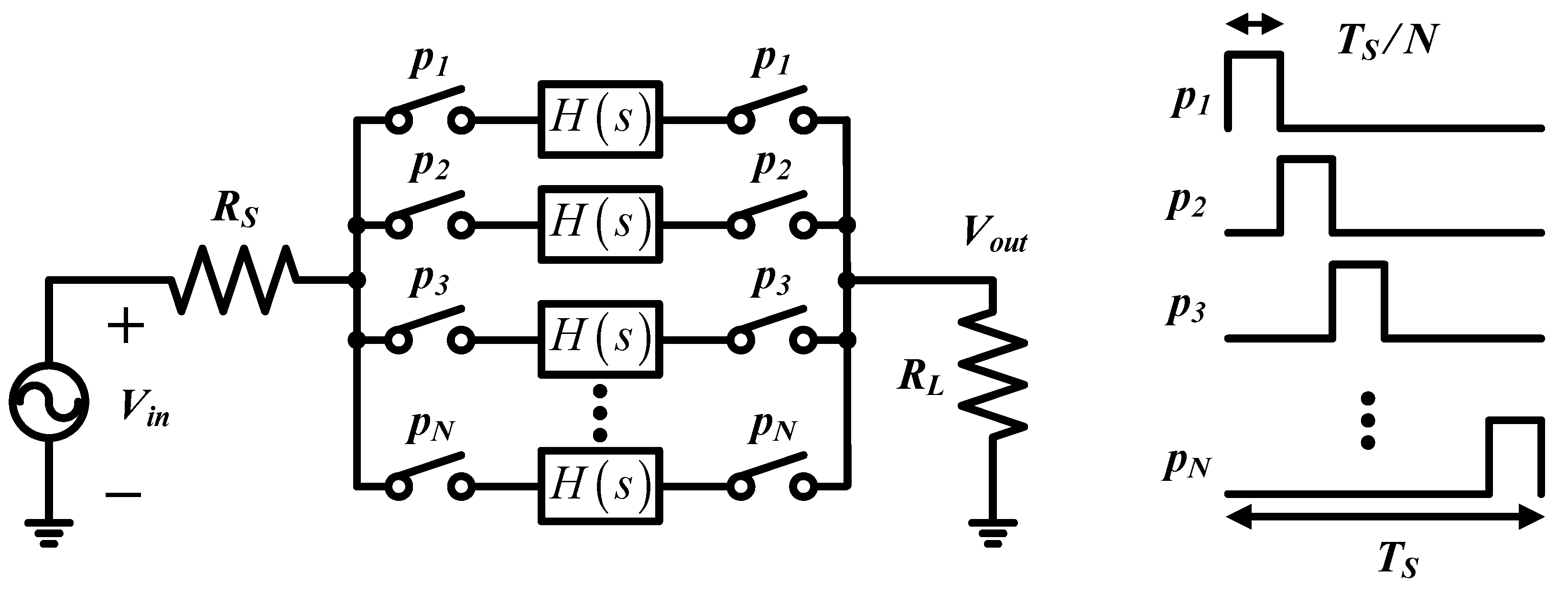
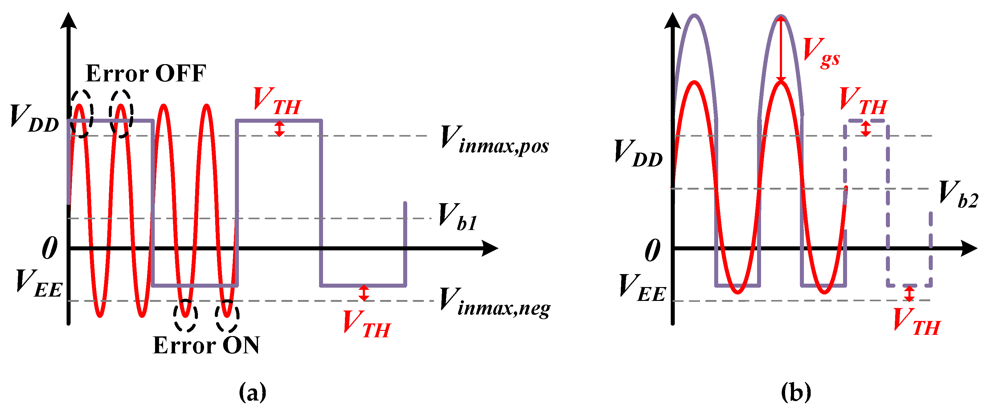
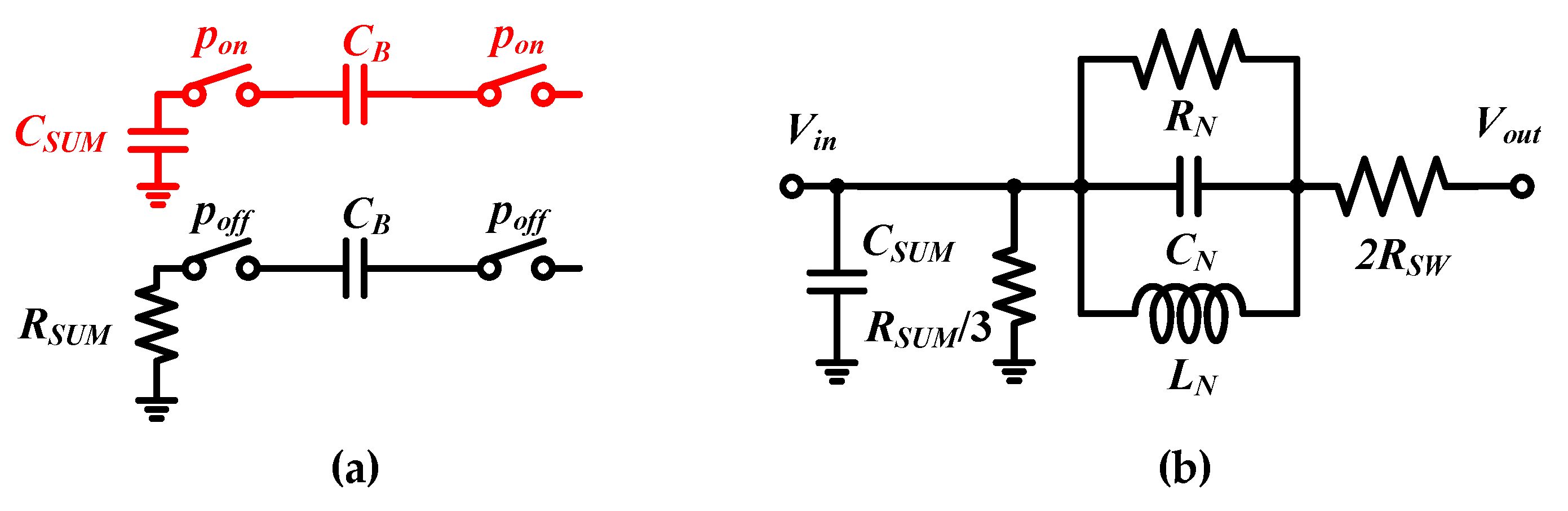
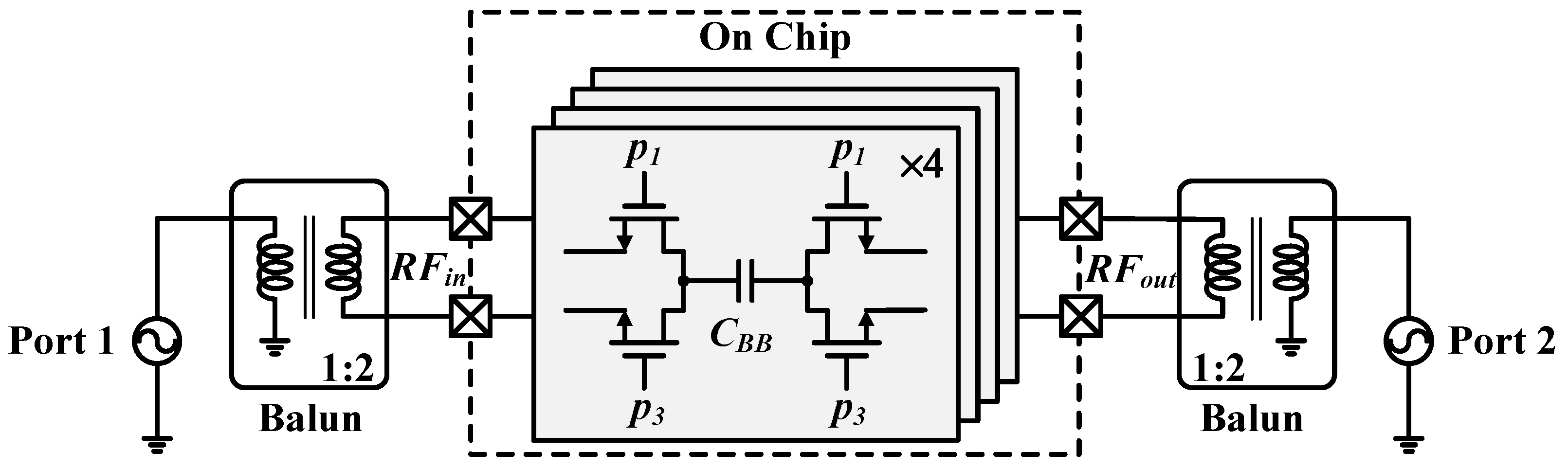
2. N-Path Notch Filter with Clock Swing Enhance

The schematic for the proposed filter is illustrated in Figure 2. The upper left corner RF section of the filter is a conventional differential 4-path notch filter, the lower part shows the LO generator including the dual-mode clock enhancement structure proposed in this paper and the upper right corner shows the clock waveform of the proposed LO generator. The proposed N-path filter is designed to achieve high linearity with a dual-mode swing-enhanced and bootstrap clock. It consists of a 4-path notch filter, a mode-switch four-phase 25%-duty-cycle boost mode, and a bootstrap mode clock generator. The RF section of the N-path filter is realized using a capacitor-sharing differential structure, which effectively suppresses even harmonics and reduces both capacitance and the chip area. The proposed notch filter suppresses leakage from the TX channel on the RX channel. The LO generator enhances filter linearity via the clock boost module, further enhances filter power handling capacity through the bootstrap module, and incorporates a clock mode switch to adapt to varying filter performance requirements.
To simplify the analysis process, the schematic of the single-ended N-path notch filter is shown in Figure 3a. The N-path notch filter can be equated to an RLC resonator as shown in Figure 3b.
The RLC model of the notch filter can be represented by a series resistance RN, capacitance CN, inductance LN, and a duty-cycle equivalence resistance RD [26]. The parameters of the RLC equivalent model are calculated as follows:
R N = N sin 2 π D + π 2 D ( 1 N D ) N ( π D 2 sin 2 π D ) R T
C N = N π 2 D m ( N sin 2 π D + π 2 D ( 1 N D ) ) C B B
L N = 1 ( 2 π f L O ) 2 C N
R T = R S + R L + 2 R S W
R D = ( 1 N D ) ( R S + R L + 2 R S W ) / ( N D )
where CBB is the N-path notch filter baseband capacitor, fLO is the clock frequency, RS and RL are the source impedance and load impedance, respectively, and RSW is the MOS switch on-resistance.
The RF filtering section of the N-path filter comprises MOS switches paired with passive capacitors to form an LTI network. In the context of the 130-nm SOI CMOS process utilized in this design, the linearity of the proposed N-path filter is limited by the gate signal swing of the MOS switches. Normally, the process determines the absolute value of the gate-to-source voltage (Vgs). In this design, simulated in 130-nm SOI CMOS technology, the maximum value of Vgs is 2.5 V. The maximum voltage of Vgs is equal to 2.5 V + Vb, where a suitable DC bias voltage Vb is applied to the input and output port through a 10 kΩ resistor Rb; the four branches are turned on alternately, and the DC bias voltage is transferred to the MOS switch drain and source, as illustrated in Figure 4a. When the input signal swing is large, the on-resistance may be increased when the switch is in the on state, and the off-resistance may be decreased when the switch is in the off state, as shown in Figure 4b.
For a four-path filter, only one path is active at a time, while the other paths are inactive. The maximum positive swing of the input signal occurs when the on-state switch is critically closed, and the positive swing is given by:
V i n , p o s = V D D V T H
where VTH is the threshold voltage of the MOS switch. The maximum negative swing of the input signal occurs when the off-state switch is critically open, and the negative swing is given by:
V i n , n e g = V E E + V T H
VEE is the clock’s low level, and VEE is a negative voltage.
The input is a sinusoidal signal, and to make the best use of the input swing, the following equation can be obtained:
V s w i n g = V i n , p o s V b = V i n , n e g + V b
this condition leads to the equation:
V b = V D D + V E E 2 V T H / 2
From this, it is possible to calculate the maximum swing of the input signal with a bias voltage of Vb as:
V s w i n g = V i n , p o s V b = V D D V E E / 2
From the above equation, the clock swing directly limits the maximum swing of the input signal. The input swing limit positively correlates with linearity with the impedance determination, according to the equation:
P i n , m a x = 10 log [ V s w i n g / 2 2 / 2 R e q u ]
where Requ is the impedance of the filter input port at the blocking frequency.
Enhancing the clock swing of the N-path filter is a key approach to improving its linearity. In this paper, we propose a method to enhance the clock swing of N-path filters in transceiver front-end filter applications, thereby improving both their linearity and dynamic range.

2.1. Mode 1: Clock Swing Enhance Module

The off-chip signal is first divided into a twofold frequency 2 × fLO of the differential signal clock, which is then processed through a shaping input divider and a frequency divider to generate a four-phase intermediate signal with a four-phase 50%-duty-cycle and 90° phase shift intermediate signal. In the conventional N-path filter clock design, the divider generates the four-phase signal, which is further processed through the gate to create a four-phase clock signal with a four-phase 25%-duty-cycle and 90° phase shift. This clock signal is then fed into the N-path filter switch gate via a clock drive buffer. To achieve maximum filter linearity, the RF section MOS switches, fabricated using the 130-nm process, employ 2.5-V MOS, yielding a clock swing from 0 to 2.5 V. Design of the core circuit in the clock section without level shifting or clock enhancement results in higher overall power consumption, which will limit the frequency bandwidth of the filter’s operating band.
In this work, the core circuit of the clock section is designed using 1.2-V MOS transistors to achieve a higher filter operating frequency and reduce the clock’s dynamic power consumption. The clock boost module shifts the clock’s high level from VDD/2 to VDD and subsequently boosts the clock’s low level from 0 to VEE.

2.1.1. Level Shifter Circuit

The schematic of the clock level shifter circuit and clock voltage waveform is illustrated in Figure 5. The input signal IN passes through the inverter 1 of the same size and the transmission gate; when the input IN is high level VDD/2, the transmission gate lifts the gate level of MN3 from VDD/2 to VDD through the capacitor C2, the source level of MP1 is VDD/2 and the gate level is VDD/2, the MP1 is turned off, and the output of the inverter 2 is 0, and the output of MN4 conducts and the output is low level 0. When the input IN is low level 0, the inverter 1 output is VDD/2 to charge the upper pole plate of capacitor C1 to VDD; at this time, MN2 conducts, the gate level of MN3 is VDD/2, MN3 turns off, the source level of MP1 is VDD/2 and the gate level is 0; MP1 conducts, and the inverter 2 outputs a high level to charge the capacitor C3 to raise the voltage of the left pole plate of C3 from VDD/2 to VDD. Therefore, the level shifter circuit realizes to lift the voltage from 0 to VDD/2 to 0 to VDD, with the fastest clock edge transitions achieved by using a small size of 0.5 μm/120 nm in the cross-coupled structure. The NMOS and PMOS transistors are sized equally to minimize delay errors in the inverter and transmission gate. The simulation results of delay errors, influenced by the MOS size for various clock frequencies, are shown in Figure 6. In this design, the NMOS size is 10 μm/120 nm, and the PMOS size is 20 μm/120 nm, reducing delay errors and lowering power consumption across the filter’s tuning range.
The 0 to VDD/2 level of the input signal is passed through C1 and C2 to generate a clock signal of VDD/2 to VDD, with C1 equal to 100 fF and C2 slightly larger equal to 105 fF, considering the driving capability of the output node. The signal after the level lift passes through the bootstrap capacitor C3, which the output level from VDD/2 to VDD extends to 0 to VDD. The size of the output switches M1, M2, and M3, as well as the capacitance value of C3, and determines the speed of the output clock edge. Considering the capacitance area, C3 is designed to be 250 fF, the size of M1 to be 10 μm/120 nm, and the size of M2 and M3 to be 20 μm/120 nm, which obtain a 60 ps clock edge. Table 1 shows the level shifter circuit terminal voltages across the transistor switches when they are in ON- and OFF-states, the choice of the switch size, and their gate voltage drives. The PMOS MP1 will withstand a maximum source-to-drain voltage difference of VDD. Thus, the PMOS MP1 in the level shifter circuit selects MOS with a 2.5-V source-drain breakdown voltage, and all other MOS are 1.2-V.
With the addition of the clock level shifter circuit, the RF section of the N-path filter continues to utilize a 2.5-V MOS design, while the clock front stage is designed with a core voltage of 1.2 V. In terms of notch filter linearity, the higher source-drain voltage of the switch in the 2.5-V MOS design can withstand greater input signal amplitudes and generate fewer nonlinear effects compared to the 1.2-V MOS design used in the clock front stage. However, a higher switching source-drain voltage also leads to increased clock power consumption. The clock boost circuit implements the low voltage design of the pre-stage circuit. The overall power consumption and linearity simulation of the clock circuit and filter are shown in Table 2. It can be seen that without using a level shifter circuit, the N-path filter switch is selected to use a 1.2-V MOS, replacing it with a 2.5-V MOS; the clock power consumption increases from 15 mW to 33.9 mW with the same clock performance, the filter B1dB is improved from −1.3 dBm to 2.1 dBm as shown in Figure 7a, and the BNF maintains a lower 0 dBm blocker with a 1.9 dB noise as shown in Figure 7b. The level shifter realizes the low power consumption of clock preamp circuits, which reduces power consumption to 21.5 mW by more than 35% and increases power consumption by only 6.5 mW compared to a 1.2-V MOS clock circuit while maintaining the same linearity and BNF performance.

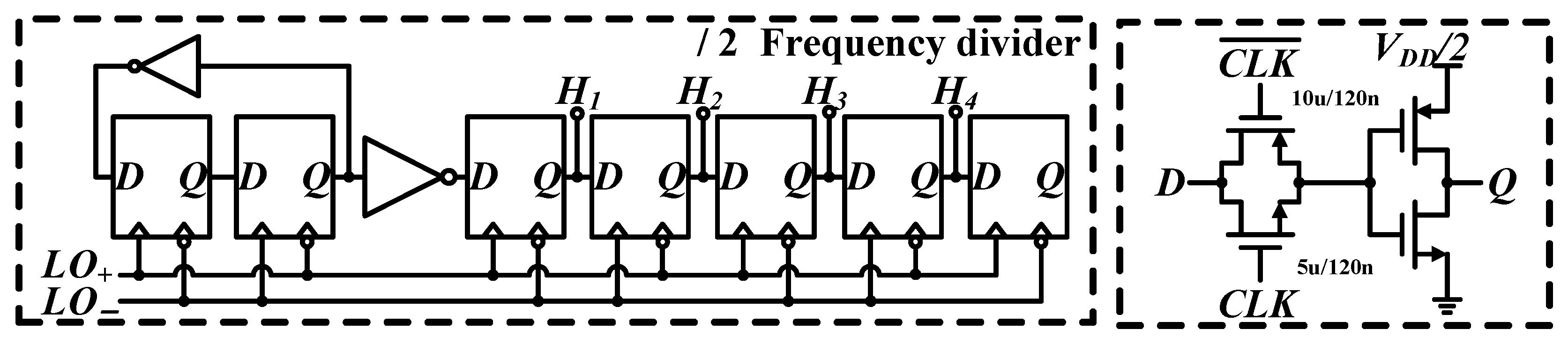
2.1.2. Clock Boost Circuit

Based on the above analysis, the clock swing directly limits the linearity of the N-path filter. To further improve its linearity, a clock boost circuit is incorporated to increase the clock swing. The circuit structure of the boost circuit is shown in Figure 8. The level shifter obtains a clock signal with the output level from 0 to VDD, which is input for the clock boost circuit. The single-ended signal input is passed through an inverter to obtain a differential signal.
When the input signal on the left-side circuit is low, it is applied to the upper pole plate of the left-side capacitor, causing the right-side circuit to output BSn-P at a high level. At this point, MN4 is on, and the gate level of MN3 is VBN, which causes MN3 to be on. The voltage on the lower pole plate of the left-side capacitor becomes VEE, thereby causing MN2 to be on. As a result, the left-side circuit outputs BSn-N at a low level with a voltage of VEE, while the corresponding right-side circuit outputs BSn-P at a high level at VDD. Similarly, when the input signal on the left-side circuit is high, the right-side circuit outputs BSn-P at a low level. In this case, MN4 in the cross-coupled structure is in the off-state, and MN5 is on. This results in a low gate level for MN3, causing MP3 to be on. At this time, the voltage of the lower pole plate of the left-side capacitor is VBN, and MN2 remains in the off state. Simultaneously, the high input signal on the left-side circuit turns MP2 on, causing the left-side circuit output BSn-N to be high with a voltage of VDD, while the corresponding production BSn-P of the right-side circuit is low with a voltage of VEE.
The input signal, with a level ranging from 0 to VDD, cannot be directly output from VEE to VDD through an inverter, as this would result in NMOS conducting continuously, which leads to a problem. The negative voltage VEE indirectly through a set of cross-complementary inverters output to the other side of the bootstrap capacitor Cbs, opposite the side of the bootstrap capacitor controlled by the input signal. To ensure the circuit works properly, VEE = −1 V in general. To better balance the NMOS and PMOS operating voltages, an additional intermediate level VBN is introduced, VBN = (VDD + VEE)/2. In the swing enhancement circuit shown in Figure 8, except for the inverters MN1 and MP1, which perform differential conversion of the input signal, the remaining transistors are symmetrically distributed and are the same size. Table 3 shows the terminal voltages across the transistor switches when they are in ON and OFF states, the choice of the switch size, and their gate voltage drives. None of the MOS source-to-drain voltages exceeded 2.5 V. To ensure that the MOS in the clock boost circuit does not break down, the minimum voltage of VEE is −2.5 V, and VBN is 0 V. The first inverter includes MN1 and MP1 to drive the bootstrap capacitors Cbs; the size of MN1 is 5 μm/220 nm, and the size of MP1 is 10 μm/220 nm. For all others, the size of NMOS is 2.5 μm/220 nm, and the size of PMOS is 5 μm/220 nm. The clock level extended via bootstrap capacitors Cbs. In the clock boost circuit, the symmetrical differential structure enables the output of single-ended differential signals to provide differential clock signals for the rear stage, saving the circuit area and power consumption. The cross-complementary inverter structure minimizes the dynamic power consumption of the circuit. The bootstrap capacitance Cbs is realized by the MOM capacitor, and the capacitance value affects the clock edge speed to balance the area and performance; in this design, Cbs is equal to 250 fF. To obtain the optimum clock operating frequency and speed, in the clock swing enhance circuit, the size of NMOS is equal to 5 μm/120 nm, and the size of PMOS is equal to 10 μm/120 nm, which obtains a 67 ps clock edge with a 17 ps increase.
Table 4 shows the clock boost circuit and filter’s overall power consumption and linearity simulation. The VEE is supplied off-chip directly at −1 V and VBN at 0.5 V to reduce the clock power consumption. The clock boost circuit increases the clock swing from VDD to (VDD + VEE), and the filter B1dB is improved from 2.1 dBm to 10 dBm, as shown in Figure 9a. The BNF maintains a lower 0dBm blocker with a 1.63 dB noise, as shown in Figure 9b, and even at 10 dBm blocker, it can maintain BNF < 2 dB, which improves the SNR of receivers at a large blocker. At the same time, the power consumption of the N-path filter clock is well controlled, and high linearity is achieved with power consumption similar to that of a traditional clock with a 2.5-V switch. The 2.5-V switch with a level shifter circuit and clock boost circuit achieves 40.2 mW clock power consumption at 500 MHz.
The clock boost circuit improves the linearity of the N-path notch filter, including the blocking power and BNF. As the clock swing increases, the clock boost module will inevitably cause the multiplexed clock edges to slow down. Figure 10a shows the clock edge rise-/fall-time and the power consumption over the RF tuning range. The longer clock rise-/fall-time is directly manifested by a decrease in the clock duty cycle, which, according to the derivation of Equation (5), leads to an increase in the passband insertion loss of the notch filter and an increase in the rejection depth. In the clock boost module, the voltage of VEE directly influences the linearity of the N-path notch filter. As shown in Figure 10b, the simulation results of the P1dB, B1dB, and IIP3 vary with VEE.
Compared to the enhanced clocking of the N-path filter in the previously published results [24], the level shifter and clock boost circuit in this design effectively enhance the N-path filter clock output swing while maintaining a low clock rise-/fall-time and consuming relatively low power, obtaining PDC/fLO = 34 mW/GHz at an operating frequency of 1.2 GHz. The proposed clock boost module is widely used in the N-path bandpass filter or N-path notch filter, which greatly improves the linearity of the filter and enhances the sensitivity of the backend receiver for the different applications in narrowband and wideband RX to reject TX leakage.

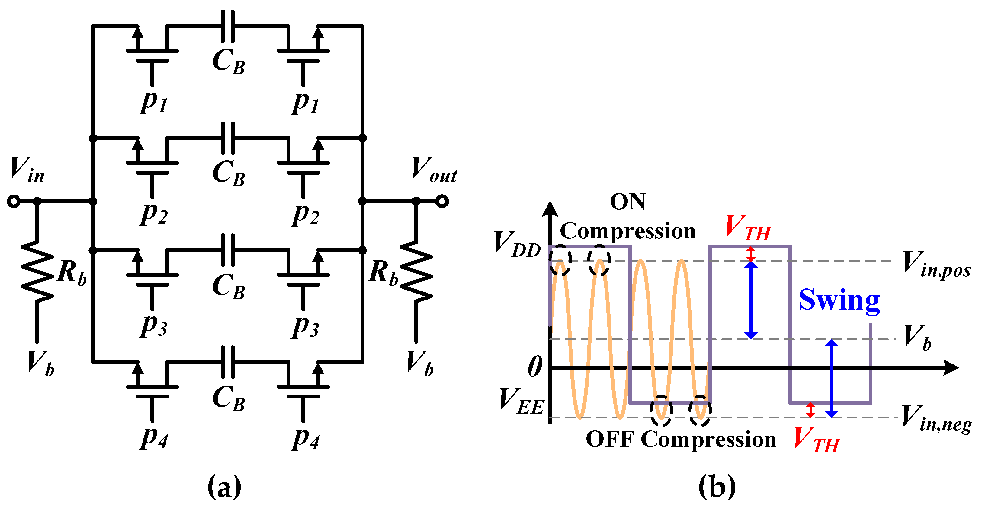
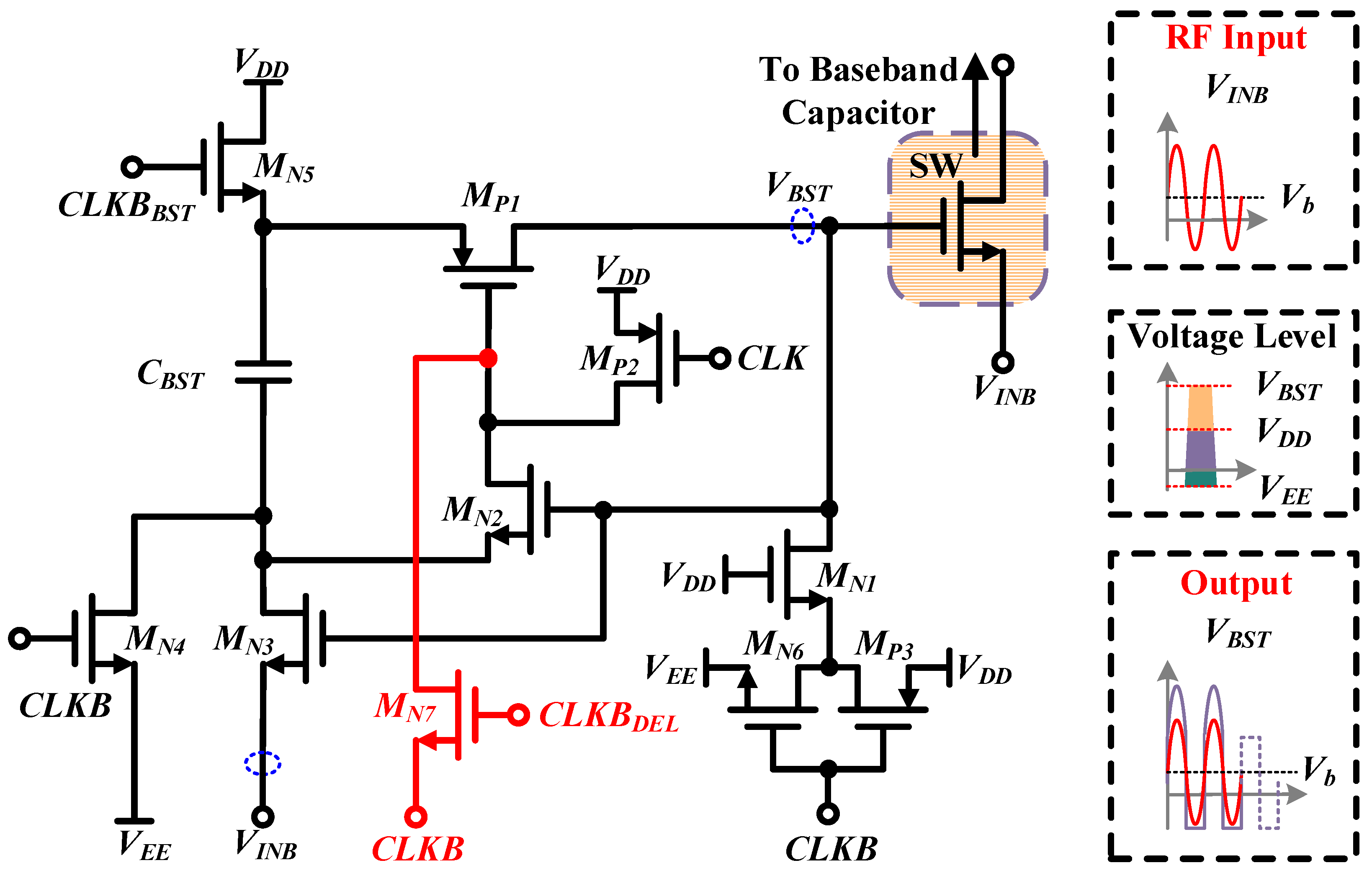
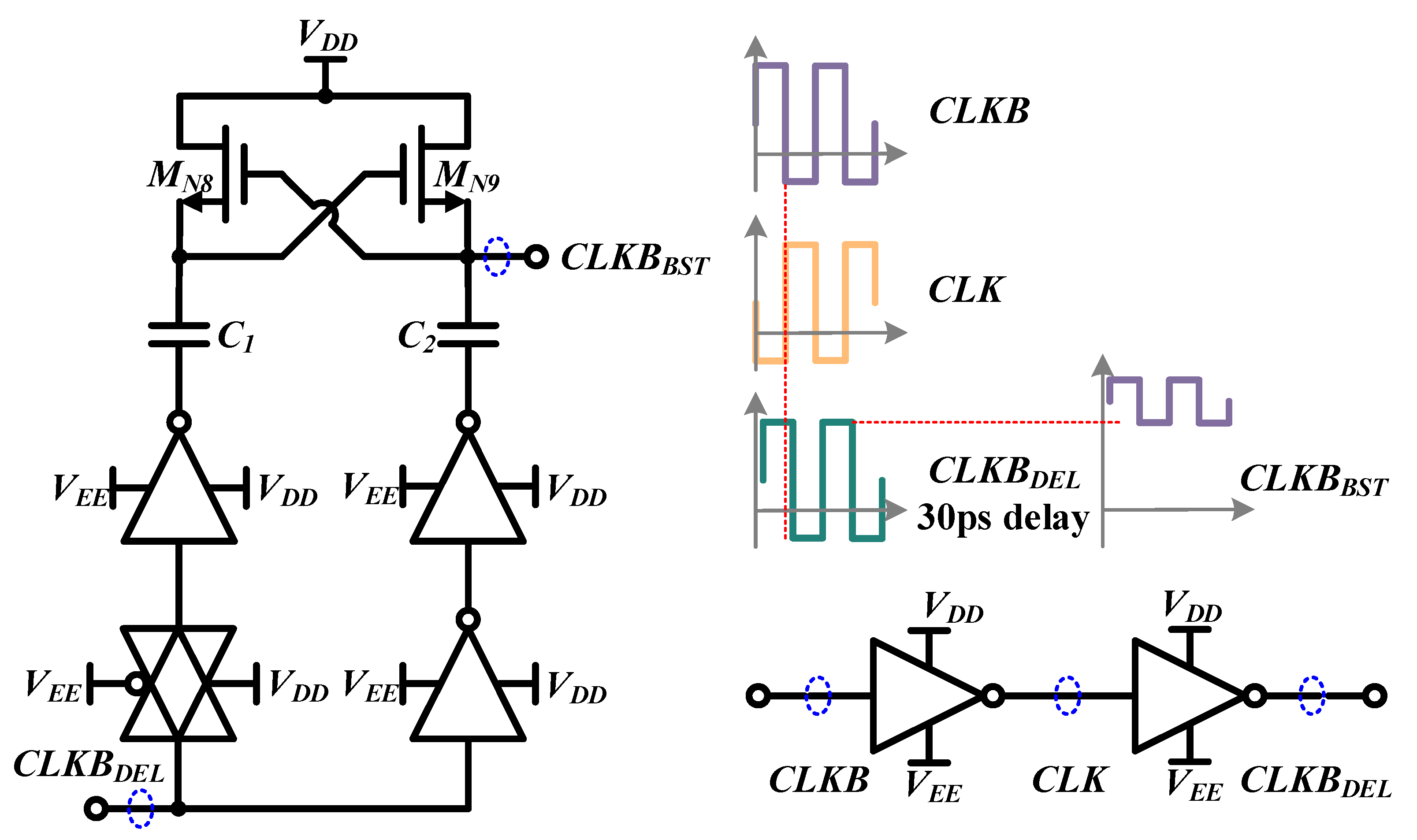
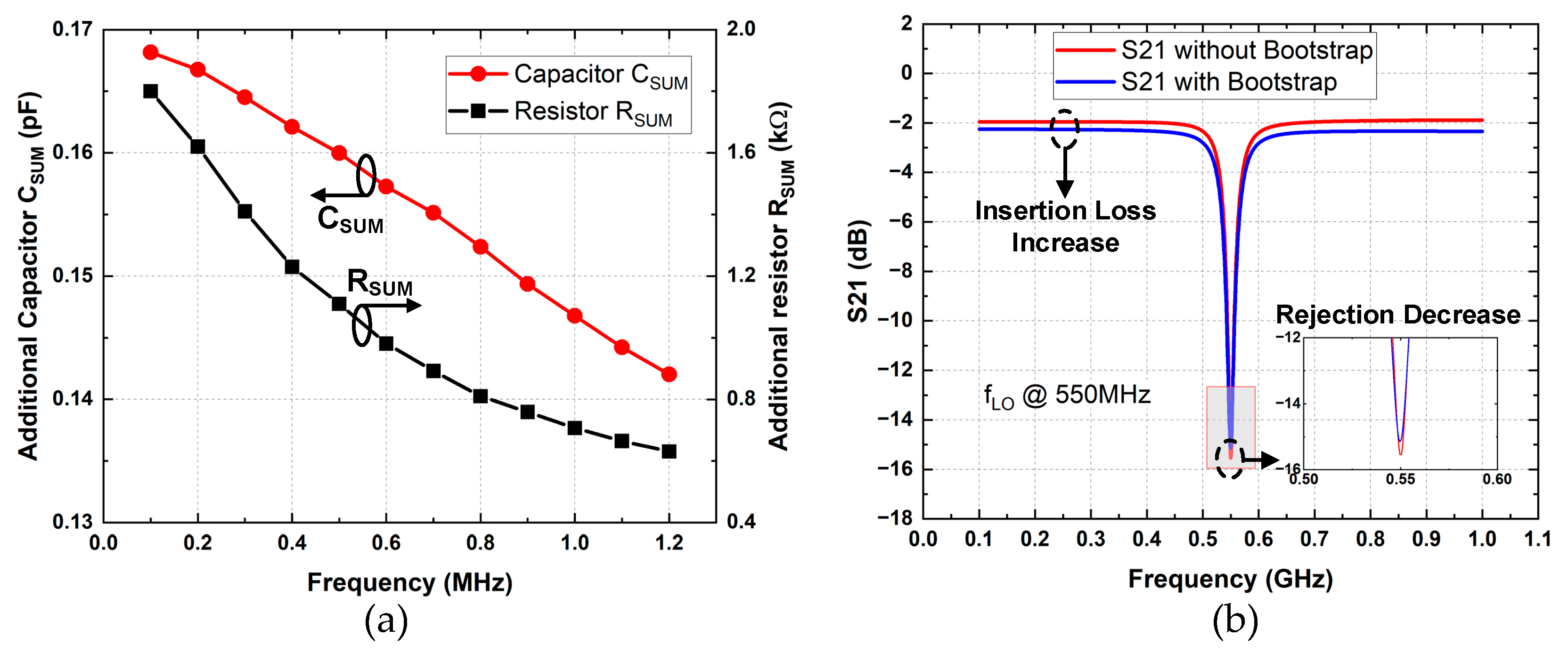
2.2. Mode 2: Clock Bootstrap Module

The above-designed clock swing enhances the module and maximizes the clock swing of the N-path notch filter as much as the process allows to improve the filter linearity. In the case of the design using 130-nm SOI CMOS, the terminal voltages of the transistors shown in Table 1 and Table 3, the clock swing is 2VDD maximum, the B1dB of the N-path notch filter is 10 dBm maximum, and the clock power consumption at the clock frequency fLO of 1.2 GHz is 33.7 mW. At a large input signal amplitude, the Vgs of the filter switch changes, and the switch on-resistance RSW changes, resulting in a strong non-linear effect. The on-resistance RSW is shown:
R S W = 1 μ C W L V D D V i n V T H )
In the event that the receiver encounters an extremely large blocker signal, the clock boost module is unable to boost the clock swing any further, which may result in an MOS breakdown. This may cause an incorrect off-state to on-state and an incorrect on-state to off-state, as shown in Figure 11a. In previous studies, a constant clock voltage difference was maintained during switch on or off by feeding the input signal to the RC combiner network in real time, an approach in which too large an input signal in the switch off-state results in a large negative bias voltage on the gate, which is not applicable to CMOS processes with 2.5-V or even lower breakdown voltages. At the same time, the excessive clock swing in the 0.15-um depletion mode GaN process leads to large clock power consumption and a slow rise-/fall-edge [27].
The improved bootstrap module in this design has a clock output equal to the superposition of the original clock signal and the input signal during the on-state of the N-path switches, maintains Vgs as a constant value in the on-state, and maintains the gate voltage as a negative voltage VEE, in the off-state of the switches, as shown in Figure 11b.
Inspired by the literature on the high-speed ADC bootstrap switch design [28], a low-latency bootstrap clock drive structure is utilized in this design for high linearity N-path filters, as shown in Figure 12. The signal processed on the RF path of the N-path filter is VINB, the switch source input signal, and the drain is connected to a baseband capacitor. During the clock-high cycle, the input signal charges the bootstrap capacitor CBST through MN3, and the maximum output VBST voltage level is VINB + VDD of the gate-driven clock, while the charging rate is related to the MN3, MN5, and CBST sizes; CBST is designed for 1 pF. During the clock low cycle, MN3 and MN5 are turned off with MP2, and MN4 discharges to the MP1 gate to accelerate the shutdown of the charging loop. The PMOS type of MP1 will result in a large clock turn-on delay [28]. To address this issue, an additional delay path is introduced in the original input bootstrap circuit. When the input clock transitions to a low level, the additional path, through MN7, directly pulls down the gate of MP1. However, without proper timing control, if MN7 is activated while MN2 and MN3 are fully on, it will turn off MP1, prematurely ending the charging of the bootstrap capacitor, and causing the bootstrap clock to fail. To prevent this, the gate of MN7 is driven by a delayed signal, in phase with the input clock, to turn off MN7. This accelerates the turn-on of MP1 in the bootstrap path, thereby increasing the rise rate of the bootstrap without enlarging the size of other MOS transistors. When the input clock is at a high level, the control switch MN3 is turned off, and the gate of the filter switch is pulled low through MN1 and the inverter MN6. The final driving voltage of the filter switch gate is then set. Similarly, the discharge edge of the clock signal is determined by the sizes of MN5 and MP1. During the discharge period, since MN1 and the inverter MN6 are on, the discharge action is faster than the signal generated after the delay through the inverter, which drives MP2. This results in a short timing overlap where both the charging loop of MP1 and the discharge loop are conducted simultaneously. This not only causes slower discharge of the filter gate bootstrap voltage but also leads to additional clock power consumption. To reduce this power consumption, the design considers reducing the sizes of the inverter MN6 and the transistor driving MP2, thereby reducing the delay.
The bootstrap voltage and delay clock generation circuit are shown in Figure 13. C1 is designed for 50 fF, and C2 is designed for 150 fF, adding an additional shutdown loop MN6, a cascaded inverter to the input clock CLKB delayed by 30 ps to produce CLKBDEL. This design shortens the falling edge of the clock after the bootstrap from 160 ps to 93 ps. The MOS size is rationally designed while considering the power consumption and speed of the clock bootstrap circuit, as shown in Table 5.
The clock bootstrap module inputs RFin into the gate drive signal through a bootstrap capacitor during the switch-on cycle. As shown in Figure 14a, for a 4-path filter with one branch in clock-on-cycle, MN3 is turned on with MP0, and the RF input from VINB can be viewed as the bootstrap capacitor CBST in series with the MOS gate-to-ground parasitic capacitance Cpara of MN3, MN4, and MN5 to form CSUM. The other three branches are in the clock-off-cycle and MN3 is off, which can be equated to a large resistor RSUM to ground with a small enough parasitic capacitance of MN3 to ground. To minimize CSUM and RSUM’s contribution to the minimum filter insertion loss, the MN3 size is 5 μm/220 nm. For the entire 4-path notch filter, the clock bootstrap module introduces an additional capacitor CSUM and three resistors RSUM at the RF inputs, as shown in Figure 14b.
To further analyze the effect of the clock bootstrap module on the performance of the filter, the input port VINB of the bootstrap circuit is simulated for different clock states, as shown in Figure 15a for the values of CSUM and RSUM at a different clock frequency fLO. The changes in filters S21 and S11 before and after the addition of the bootstrap module are shown in Figure 15b.

2.3. Frequency Divider

Figure 16 illustrates the schematic of the four-phase 25%-duty-cycle frequency divider. It uses an off-chip differential sinusoidal clock, LO+ and LO. The divider-by-two-ring counter circuit uses D flip-flop; the size of NMOS is 5 μm/120 nm and the size of PMOS is 10 μm/120 nm.

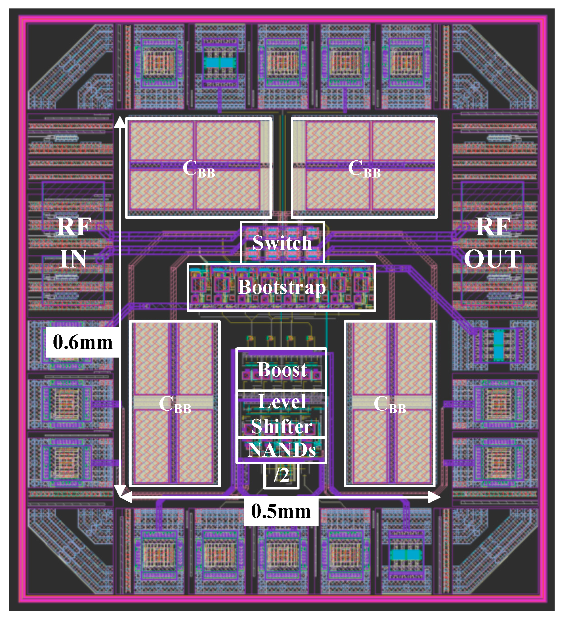
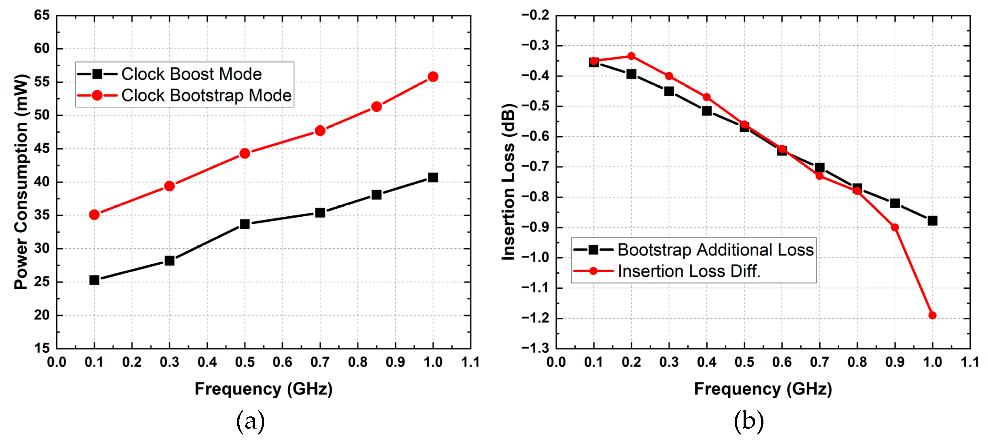
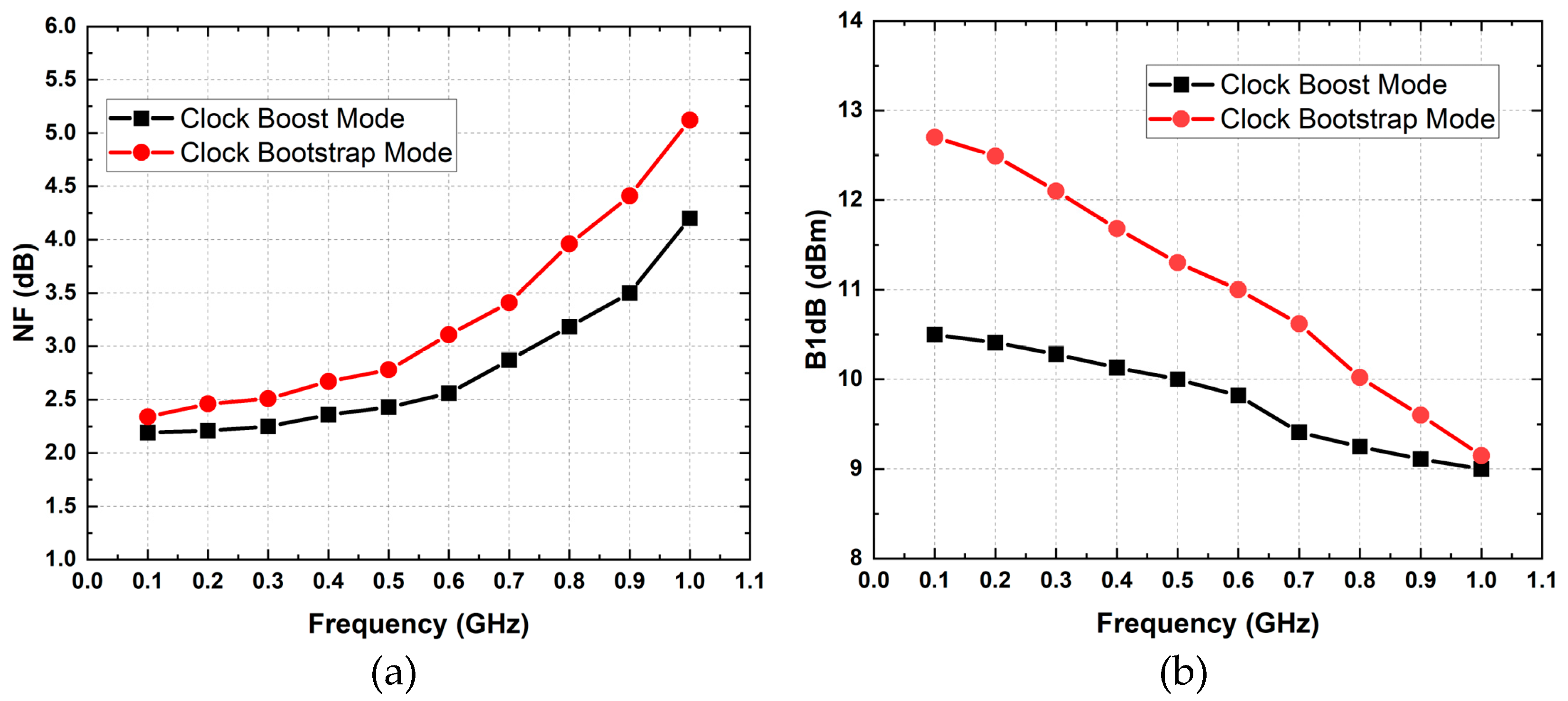
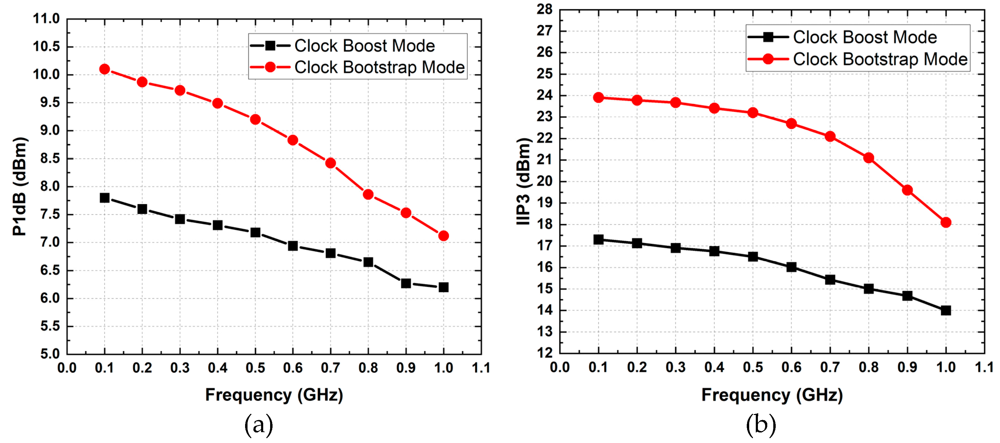
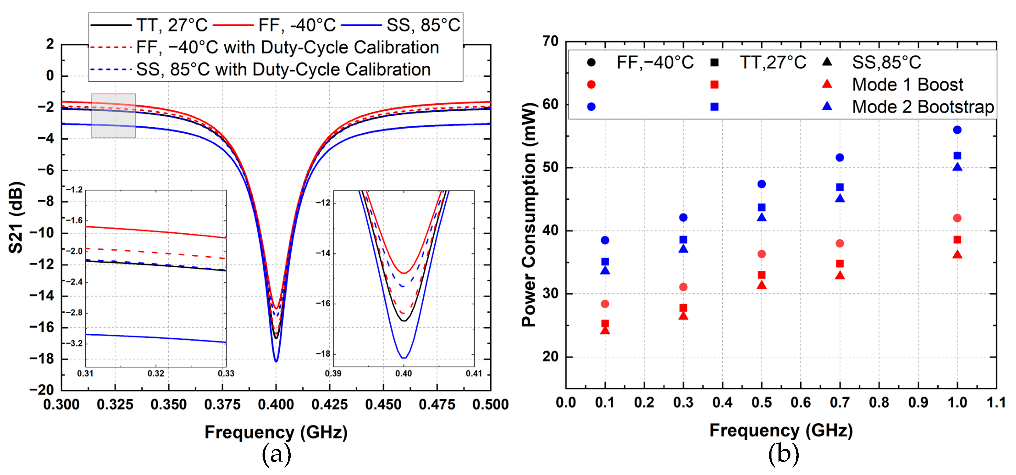
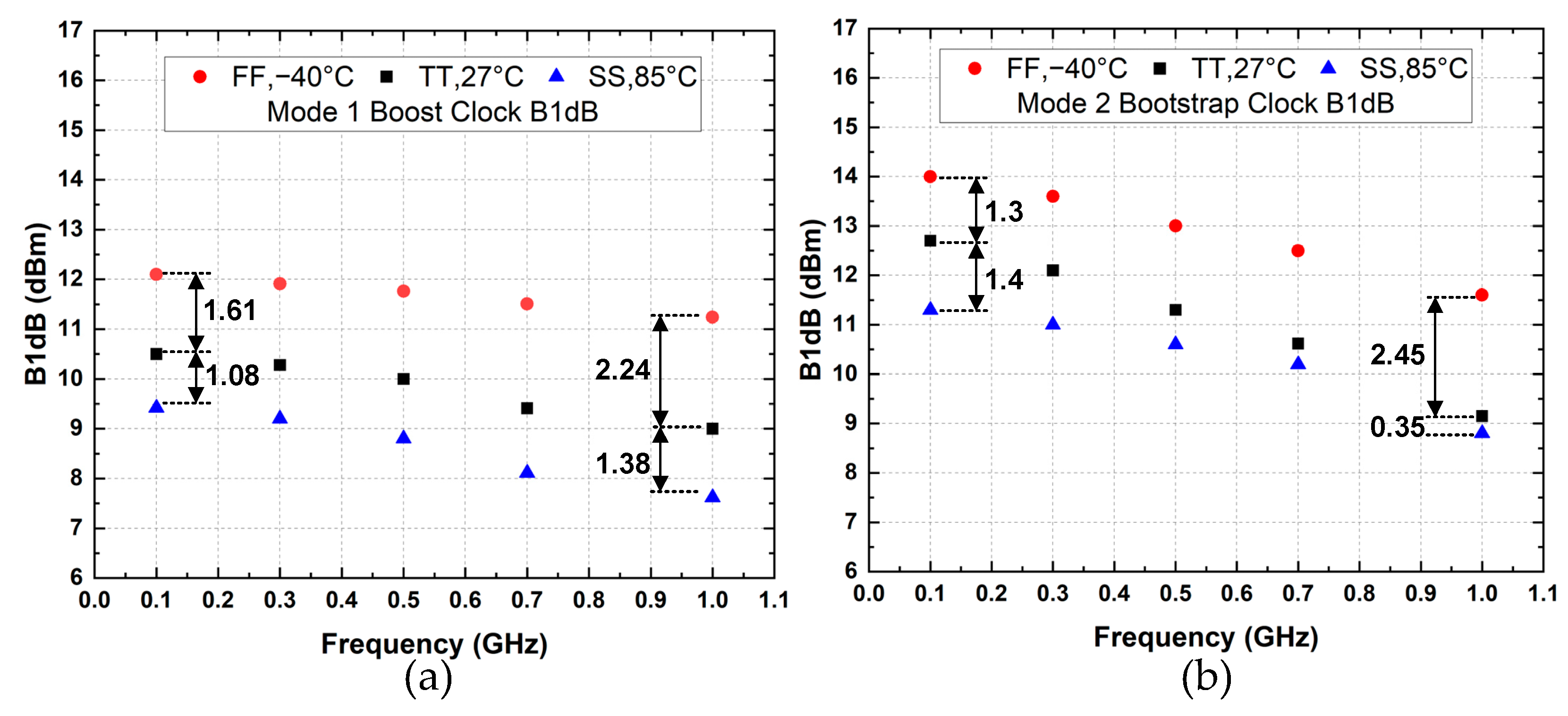
3. Post-Layout Simulation Results

The proposed N-path notch filter with a clock boost and bootstrap module is post-layout simulated in a 130-nm SOI CMOS process. Its total area is 0.6 mm × 0.5 mm, not including the ESD and pad. The final layout is shown in Figure 17. All on-chip capacitors are realized using MIM capacitors. Figure 18 shows the schematic diagram of the proposed differential notch filter with two off-chip 1:2 baluns.

3.1. S-Parameters

S21 describes the proposed notch filter transmission characteristics from port 1 to port 2, in which the passband insertion loss and the depth of rejection for small signals can be seen. S11 describes the reflection characteristics of the small signal port 1 at the input of the proposed notch filter. Figure 19 shows the S21 simulation results of the proposed filter. The passband insertion loss of the notch filter varies from −1.89 dB to −3.07 dB in the clock boost mode and varies from −2.04 dB to −4.85 dB in the bootstrap mode, while the passband bandwidth is 32 MHz. The S11 simulation results of the proposed filter are shown in Figure 20; the passband S11 < −8 dB in boost mode and S11 < −12 dB in bootstrap mode over the RF tuning range. The power consumption is simulated to range from 25.3 to 40.7 mW in the clock boost mode and simulated to range from 35.1 to 55.1 mW in the clock bootstrap mode within the 0.1 to 1.0 GHz RF tuning range, as shown in Figure 21a. The insertion loss increases at high frequencies in both modes due to the clock quality, with more pronounced deterioration in the bootstrap mode. There is a difference in the insertion loss between the clock boost mode and clock bootstrap mode. According to previous analysis, the clock bootstrap mode introduces additional parasitic capacitance CSUM and parasitic resistance RSUM, resulting in additional insertion loss, and the difference in insertion loss between the two modes coincides with it, as shown in Figure 21b. The rational design of bootstrap circuit device parameters balances the bootstrap speed, power consumption, and insertion loss.

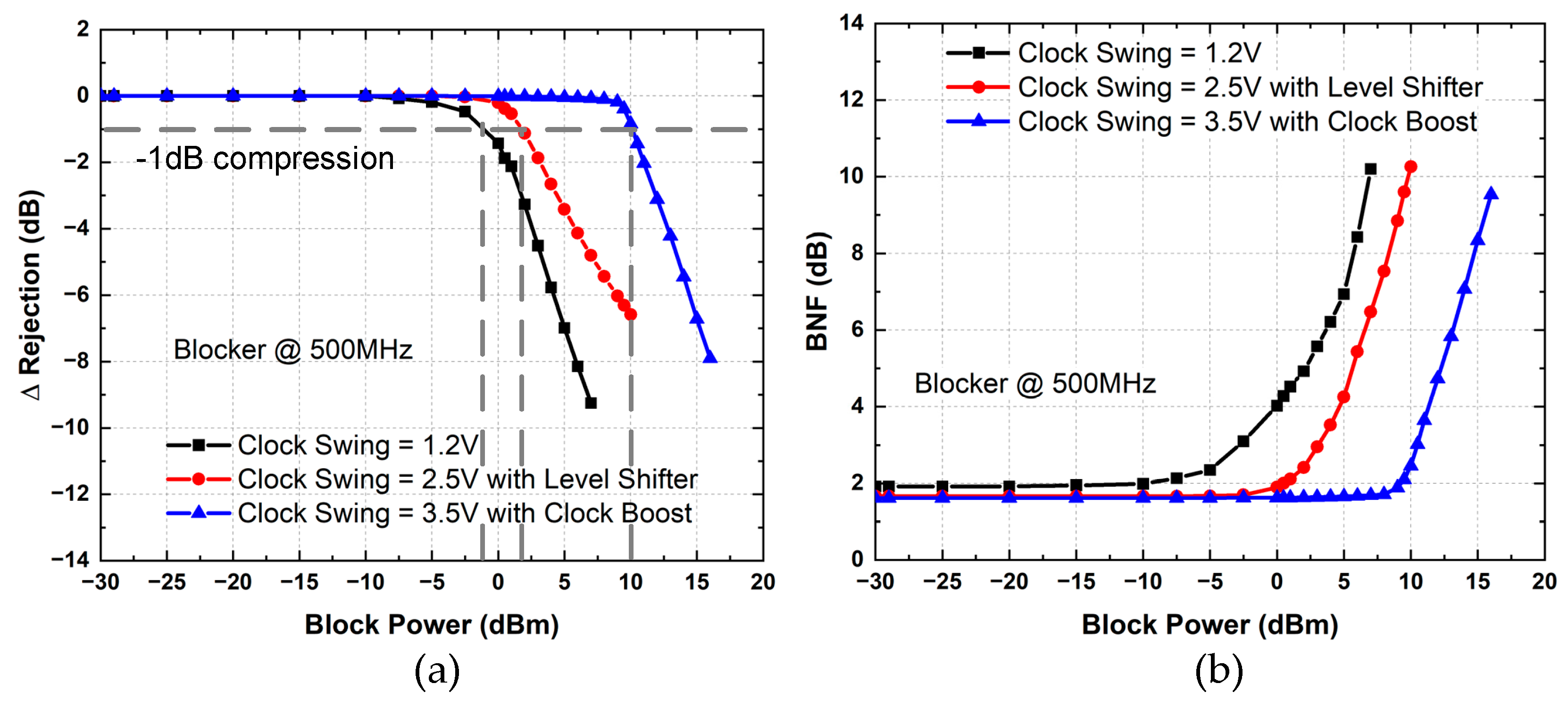
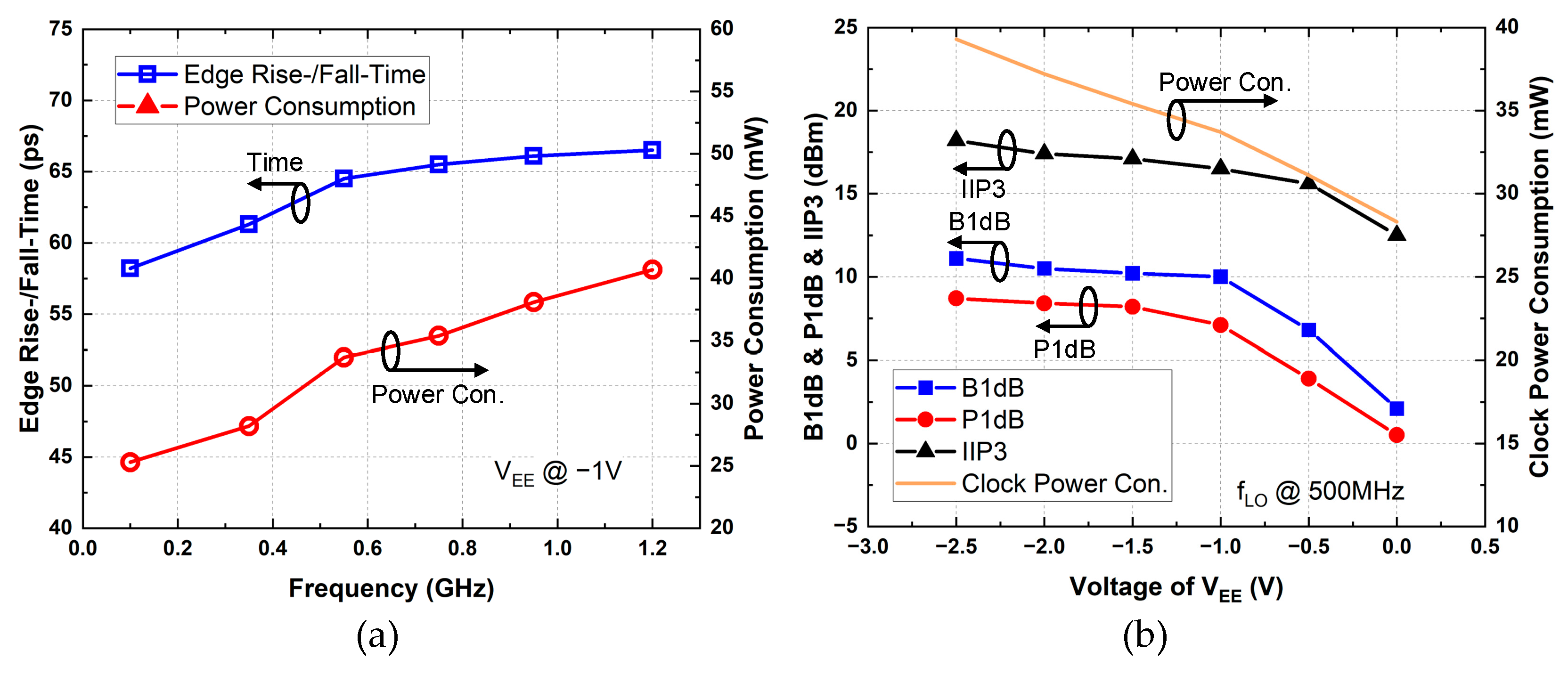
3.2. Linearity and NF

The simulated result of NF is shown in Figure 22a; the passband NF of the proposed filter varies from 2.19 to 4.2 dB working in swing boost mode and varies from 2.34 to 5.12 dB working in bootstrap mode. A single tone at fLO is used to measure B1dB, which varies from 9 to 10.5 dBm working in swing boost mode and varies from 9.15 to 12.7 dBm working in bootstrap mode, as shown in Figure 22b. A single tone at fLO + 75 MHz is used to measure P1dB in the passband, which varies from 6.2 to 7.8 dBm working in swing boost mode and varies from 7.12 to 10.1 dBm working in bootstrap mode as shown in Figure 23a. The third-order input-intercept-point (IIP3) profile is measured by injecting two-tone tests with a frequency at fLO + 75 MHz and fLO + 76 MHz. As shown in Figure 23b, the IIP3 varies from 14 to 17.3 dBm working in swing boost mode and varies from 18.1 to 23.9 dBm working in bootstrap mode.
The impact of PVT on the performance primarily affects the MOS switching speed and capacitance values. Since the capacitance values only influence the bandwidth of the N-path filter, we focused on the performance and power consumption variations of the filter under two extreme process conditions (FF, −40 °C and SS, 85 °C) in the post-layout simulations. Under FF, −40 °C and SS, 85 °C conditions, which correspond to the fastest and slowest MOS performance, the impact on the filter’s S21 is mainly observed in the insertion loss and rejection depth as shown in Figure 24a. Without duty-cycle calibration, FF, −40 °C results in shorter clock rise/fall times and an increased clock duty cycle, leading to a reduced insertion loss and attenuation. With duty-cycle calibration, the performance is nearly identical to that at TT, 27 °C. On the other hand, SS, 85 °C causes longer clock rise/fall times and a reduced clock duty cycle, resulting in a conduction dead zone that increases both the insertion loss and rejection depth. With duty-cycle calibration, the increased MOS on-resistance leads to a 1 dB to 2 dB decrease in the rejection depth compared to TT, 27 °C. As shown in Figure 24b, under two extreme process conditions (FF, −40 °C and SS, 85 °C), the clock power consumption variation across different modes is less than 5 mW.
As shown in Figure 25, under FF, −40 °C conditions, the B1dB of both clock modes increased by 1 dB to 2.5 dB, and the performance degradation rate slowed down significantly as the clock frequency increased. Under SS, 85 °C conditions, the B1dB of both clock modes decreased by no more than 1.5 dB. For the Mode 2 clock bootstrap, the high-frequency performance impact was minimal, with B1dB only dropping by 0.35 dB. This indicates that faster MOS speeds lead to a more significant performance improvement in the Mode 2 bootstrap configuration.
Table 6 summarizes the performance of the proposed notch filter and compares the simulation results with a state-of-the-art N-path notch filter. Compared to the N-path notch filter with a traditional clock generator presented in [26,29], the proposed clock topology enhanced the clock swing from 2.5 V to 3.5 V and even higher to 3.5 V + RFIN adaptive based on input; it dramatically improved the filter linearity including B1dB, P1dB, and IIP3. Compared to the charge-pump-based swing boost clock [24], the proposed notch filter limitation of the clock swing in view of the operational stability gets close to the PDC/fLO. The proposed clock offers superior clock quality compared to the previous works, as evidenced by the reduced insertion loss and noise figure of the filter. Our design has no on-chip inductors and achieves similar or better filter linearity performance. Compared to the N-path bandpass filter series notch filter with a swing boost clock [25], the proposed filter obtains lower clock power consumption under a different input signal amplitude and can flexibly select the swing boost mode or bootstrap mode to reduce power consumption.

4. Conclusions

This paper presents a dual-mode clock enhancement technology to design an N-path notch filter to obtain high linearity designed and post-layout simulated using the 130-nm SOI CMOS process. In Mode 1, the clock swing boost mode, the boost module extends the clock swing from 2.5 V to 3.5 V, increasing B1dB to 9 dBm with comparable power consumption and NF compared to traditional N-path filters. In Mode 2, the clock bootstrap mode, on top of the clock boost in Mode 1, along with the 15 mW increase in power consumption, the filter IIP3 reaches a 23.9 dBm increase 6 dB compared to the traditional N-path filter, and both B1dB and P1dB increase by 2.5 dB from Mode 1; the bootstrap module results in an additional 1 dB insertion loss and poorer linearity performance at high frequencies. Flexible switching of clock operating modes in different input modes results in reasonable deployment of clock power consumption. This clock enhancement technique can be applied to other switch-capacitor-based structures, including N-path bandpass and notch filters, and can improve the linearity of these filters as well.

Author Contributions

Conceptualization, X.L.; methodology, X.L.; software, X.L. and H.Z.; validation, X.L. and H.Z.; formal analysis, X.L.; investigation, X.L.; resources, H.Z., G.W. and L.Z.; data curation, X.L. and H.Z.; writing—original draft preparation, X.L.; writing—review and editing, X.L., S.X., H.Z., G.W. and L.Z.; visualization, X.L.; supervision, G.W. and L.Z.; project administration, L.Z.; funding acquisition, G.W. and L.Z. All authors have read and agreed to the published version of the manuscript.

Funding

This research received no external funding.

Data Availability Statement

The datasets produced and/or analyzed in the present study are available from the corresponding author upon reasonable request.

Conflicts of Interest

The authors declare no conflicts of interest.

Abbreviations

The following abbreviations are used in this manuscript:
IoTInternet of Things
TXTransmitter
RXReceiver
LNALow noise amplifier
B1dBBlocker 1-dB compression point
P1dB1-dB compression point
IIP3Third-order input-intercept-point
SNRSignal-to-noise ratio
LTILinear time-invariant
SCSwitched capacitor
SAWSurface acoustic wave
BRFBand reject filters
BPFBandpass filter
LOLocal oscillator
VgsGate-to-source voltage
NFNoise figure
BNFBlocker noise figure

References

  1. Wang, P.-H.P.; Mercier, P.P. A Dual-Mode Wi-Fi/BLE Wake-Up Receiver. IEEE J. Solid-State Circuits 2021, 56, 1288–1298. [Google Scholar] [CrossRef]
  2. Jain, P.; Gaba, G.S.; Kansal, L.; Ngo, S. 5G and Beyond. In Proceedings of the 2018 International Conference on Communication and Signal Processing (ICCSP), Chennai, India, 3–5 April 2018; pp. 0878–0882. [Google Scholar] [CrossRef]
  3. Mugerwa, D.; Nam, Y.; Choi, H.; Shin, Y.; Lee, E. Adaptive Mobility-Based IoT LoRa Clustering Communication Scheme. Electronics 2024, 13, 2052. [Google Scholar] [CrossRef]
  4. Sun, J.; Chen, D.; Wang, Q.; Lei, C.; Wang, M.; Li, Z.; Xiao, Y.; Zhang, W.; Liu, J. Key Issues on Integrating 5G into Industrial Systems. Electronics 2024, 13, 2048. [Google Scholar] [CrossRef]
  5. Atzori, L.; Iera, A.; Morabito, G. The internet of things: A survey. Comput. Netw. 2010, 54, 2787–2805. [Google Scholar] [CrossRef]
  6. Shahid, N.; Aneja, S. Internet of Things: Vision, application areas and research challenges. In Proceedings of the 2017 International Conference on I-SMAC (IoT in Social, Mobile, Analytics and Cloud) (I-SMAC), Palladam, India, 10–11 February 2017; Volume 10, pp. 583–587. [Google Scholar] [CrossRef]
  7. Lee, C.; Fumagalli, A. Internet of Things Security—Multilayered Method For End to End Data Communications Over Cellular Networks. In Proceedings of the 2019 IEEE 5th World Forum on Internet of Things (WF-IoT), Limerick, Ireland, 15–18 April 2019; pp. 24–28. [Google Scholar] [CrossRef]
  8. Fortino, G.; Russo, W.; Savaglio, C.; Viroli, M.; Zhou, M. Opportunistic cyberphysical services: A novel paradigm for the future Internet of Things. In Proceedings of the 2018 IEEE 4th World Forum on Internet of Things (WF-IoT), Singapore, 5–8 May 2018; pp. 488–492. [Google Scholar] [CrossRef]
  9. Lee, H.; Heo, J.; Hong, D. A New GNSS-based Channel Estimation Strategy for LEO Satellite Communication Systems. In Proceedings of the 2023 IEEE 97th Vehicular Technology Conference (VTC2023-Spring), Florence, Italy, 20–23 June 2023; pp. 1–5. [Google Scholar] [CrossRef]
  10. Li, B.; Li, Z.; Zhou, H.; Chen, X.; Peng, Y.; Yu, P.; Wang, Y.; Feng, X. A System of Power Emergency Communication System Based BDS and LEO Satellite. In Proceedings of the 2021 Computing, Communications and IoT Applications (ComComAp), Shenzhen, China, 26–28 November 2021; pp. 286–291. [Google Scholar] [CrossRef]
  11. Filjar, R.; Huljenic, D. Positioning augmentation using synergy between telecommunications networks and satellite positioning methods. In Proceedings of the 17th International Conference on Applied Electromagnetics and Communications, 2003. ICECom 2003, Dubrovnik, Croatia, 1–3 October 2003; pp. 37–40. [Google Scholar] [CrossRef]
  12. Egea-Roca, D.; Arizabaleta-Diez, M.; Pany, T.; Antreich, F.; Lopez-Salcedo, J.A.; Paonni, M.; Seco-Granados, G. GNSS User Technology: State-of-the-Art and Future Trends. IEEE Access 2022, 10, 39939–39968. [Google Scholar] [CrossRef]
  13. Yoo, B.-Y.; Park, J.-H.; Yang, J.-R. Quasi-Circulator Using an Asymmetric Coupler for Tx Leakage Cancellation. Electronics 2018, 7, 173. [Google Scholar] [CrossRef]
  14. Emon, M.Z.A.; Salim, K.M.; Chowdhury, M.I.B. Design and Analysis of a High-Gain, Low-Noise, and Low-Power Analog Front End for Electrocardiogram Acquisition in 45 nm Technology Using gm/ID Method. Electronics 2024, 13, 2190. [Google Scholar] [CrossRef]
  15. Haq, T.; Koziel, S.; Pietrenko-Dabrowska, A. Resonator-Loaded Waveguide Notch Filters with Broad Tuning Range and Additive-Manufacturing-Based Operating Frequency Adjustment Procedure. Electronics 2023, 12, 4486. [Google Scholar] [CrossRef]
  16. Soorapanth, T.; Wong, S. A 0-dB IL 2140 ± 30 MHz bandpass filter utilizing Q-enhanced spiral inductors in standard CMOS. IEEE J. Solid-State Circuits 2002, 37, 579–586. [Google Scholar] [CrossRef]
  17. Franks, L.E.; Sandberg, I.W. An alternative approach to the realization of network transfer functions: The N-path filter. Bell Syst. Tech. J. 1960, 39, 1321–1350. [Google Scholar] [CrossRef]
  18. Lin, Z.; Mak, P.-I.; Martins, R.P. Analysis and Modeling of a Gain-Boosted N-Path Switched-Capacitor Bandpass Filter. IEEE Trans. Circuits Syst. I: Regul. Pap. 2014, 61, 2560–2568. [Google Scholar] [CrossRef]
  19. Qi, G.; Mak, P.-I. A 0.5-to-1.5GHz BW-Extended Gain-Boosted N-Path Filter Using a Switched gm−C Network Achieving 50 MHz BW and 18.2 dBm OB-IIP3. In Proceedings of the 2023 IEEE Asian Solid-State Circuits Conference (A-SSCC), Haikou, China, 5–8 November 2023; pp. 1–3. [Google Scholar] [CrossRef]
  20. Luo, C.-K.; Gudem, P.S.; Buckwalter, J.F. A 0.2–3.6-GHz 10-dBm B1dB 29-dBm IIP3 Tunable Filter for Transmit Leakage Suppression in SAW-Less 3G/4G FDD Receivers. IEEE Trans. Microw. Theory Tech. 2015, 63, 3514–3524. [Google Scholar] [CrossRef]
  21. Ghaffari, A.; Klumperink, E.A.M.; Nauta, B. Tunable N-Path Notch Filters for Blocker Suppression: Modeling and Verification. IEEE J. Solid-State Circuits 2013, 48, 1370–1382. [Google Scholar] [CrossRef]
  22. Nagulu, A.; Yi, M.; Zhuang, Y.; Garikapati, S.; Krishnaswamy, H. A 1-to-5GHz All-Passive Frequency-Translational 4th-Order N-path Filter with Low-Power Clock Boosting for High Linearity and Relaxed Pdc-Frequency Trade-Off. In Proceedings of the 2023 IEEE International Solid-State Circuits Conference (ISSCC), San Francisco, CA, USA, 19–23 February 2023; pp. 378–380. [Google Scholar] [CrossRef]
  23. Desta, N.; Cohen, E. A 0.15 um Depletion Mode GaN Bootstrapped N-path Filter with 23dBm Inband Blocker Handling. In Proceedings of the 2022 Asia-Pacific Microwave Conference (APMC), Yokohama, Japan, 29 November–2 December 2022; pp. 746–748. [Google Scholar] [CrossRef]
  24. Khorshidian, M.; Reiskarimian, N.; Krishnaswamy, H. 29.4 High-Performance Isolators and Notch Filters Based on N-Path Negative Transresistance. In Proceedings of the 2020 IEEE International Solid-State Circuits Conference—(ISSCC), San Francisco, CA, USA, 16–20 February 2020; pp. 446–448. [Google Scholar] [CrossRef]
  25. Devarajan, S.; Singer, L.; Kelly, D.; Pan, T.; Silva, J.; Brunsilius, J.; Rey-Losada, D.; Murden, F.; Speir, C.; Bray, J.; et al. A 12-b 10-GS/s Interleaved Pipeline ADC in 28-nm CMOS Technology. IEEE J. Solid-State Circuits 2017, 52, 3204–3218. [Google Scholar] [CrossRef]
  26. Ma, D.; Dai, F.F. A 7.27 GHz Q-Enhanced Low Noise Amplifier RFIC with 70 dB Image Rejection Ratio. IEEE Microw. Wirel. Compon. Lett. 2010, 20, 456–458. [Google Scholar] [CrossRef]
  27. Abdulaziz, M.; Klumperink, E.A.M.; Nauta, B.; Sjoland, H. Improving Receiver Close-In Blocker Tolerance by Baseband GmC Notch Filtering. IEEE Trans. Circuits Syst. I Regul. Pap. 2019, 66, 885–896. [Google Scholar] [CrossRef]
  28. Lien, Y.; Klumperink, E.; Tenbroek, B.; Strange, J.; Nauta, B. 24.3 A high-linearity CMOS receiver achieving +44 dBm IIP3 and +13 dBm B1dB for SAW-less LTE radio. In Proceedings of the 2017 IEEE International Solid-State Circuits Conference (ISSCC), San Francisco, CA, USA, 5–9 February 2017; pp. 412–413. [Google Scholar] [CrossRef]
  29. Purushothaman, V.K.; Klumperink, E.A.M.; Clavera, B.T.; Nauta, B. A Fully Passive RF Front End with 13-dB Gain Exploiting Implicit Capacitive Stacking in a Bottom-Plate N-Path Filter/Mixer. IEEE J. Solid-State Circuits 2020, 55, 1139–1150. [Google Scholar] [CrossRef]
Figure 1. N-path filter basic structure.
Electronics 14 01008 g001
Figure 2. Block diagram of the proposed N-path filter with clock enhancement.
Electronics 14 01008 g002
Figure 3. (a) The schematic of the N-path notch filter. (b) Equivalent single-ended circuit.
Electronics 14 01008 g003
Figure 4. (a) The schematic of the N-path notch filter with source-drain bias voltage. (b) The large RFIN causes compression.
Electronics 14 01008 g004
Figure 5. The schematic of the level shifter circuit and clock voltage waveform.
Electronics 14 01008 g005
Figure 6. Simulation results of the delay error by the MOS size for clock frequency.
Electronics 14 01008 g006
Figure 7. (a) Simulation results of rejection versus block power at fLO = 500 MHz; (b) BNF at fLO = 500 MHz.
Electronics 14 01008 g007
Figure 8. The schematic of the clock boost circuit and clock voltage waveform.
Electronics 14 01008 g008
Figure 9. (a) Rejection versus block power at fLO = 500 MHz; (b) BNF at fLO = 500 MHz.
Electronics 14 01008 g009
Figure 10. (a) Rise-/fall-time and clock power consumption versus clock frequency. (b) B1dB, P1dB, IIP3, and clock power consumption versus the boost negative voltage of VEE.
Electronics 14 01008 g010
Figure 11. (a) Circuit diagram of switch driven with a boost clock. (b) Circuit diagram of switch driven with a bootstrap clock.
Electronics 14 01008 g011
Figure 12. The schematic of the clock bootstrap circuit and clock voltage waveform.
Electronics 14 01008 g012
Figure 13. The schematic of the clock delay circuit and waveform.
Electronics 14 01008 g013
Figure 14. (a) Equivalence of bootstrap capacitors in different clock states. (b) Equivalence of additional capacitor CSUM and three resistors RSUM to N-path notch filter.
Electronics 14 01008 g014
Figure 15. (a) The additional capacitor CSUM and resistor RSUM versus clock frequency fLO. (b) S21 versus clock boost and bootstrap module at clock frequency fLO = 500 MHz.
Electronics 14 01008 g015
Figure 16. The schematic of the four-phase 25%-duty-cycle frequency divider.
Electronics 14 01008 g016
Figure 17. A layout photograph of the proposed N-path notch filter.
Electronics 14 01008 g017
Figure 18. A schematic diagram of the proposed differential notch filter with two off-chip 1:2 baluns.
Electronics 14 01008 g018
Figure 19. The S21 simulation results of the proposed filter with boost and bootstrap mode.
Electronics 14 01008 g019
Figure 20. The S11 simulation results of the proposed filter with boost and bootstrap mode.
Electronics 14 01008 g020
Figure 21. (a) The power consumption of clock boost mode and clock bootstrap mode. (b) The insertion loss difference and clock bootstrap mode additional insertion loss.
Electronics 14 01008 g021
Figure 22. (a) Simulation results of NF in boost vs. bootstrap mode. (b) Simulation results of B1dB in boost vs. bootstrap mode.
Electronics 14 01008 g022
Figure 23. (a) Simulation results of P1dB in boost vs. bootstrap mode. (b) Simulation results of IIP3 in boost vs. bootstrap mode.
Electronics 14 01008 g023
Figure 24. (a) Simulation results of S21 Mode 1 boost clock fLO = 400 MHz with PVT. (b) Simulation results of Mode 1 boost clock and Mode 2 bootstrap clock power consumption with PVT.
Electronics 14 01008 g024
Figure 25. (a) Simulation results of Mode 1 boost clock B1dB with PVT. (b) Simulation results of Mode 2 bootstrap clock B1dB with PVT.
Electronics 14 01008 g025
Table 1. Terminal voltages of the transistors in the level shifter circuit.
TransistorsVsource,ONVdrain,ONVsource,OFFVdrain,OFFVgate LevelSize
MN1VDD/2VDD/2VDDVDD/2VDD − VDD/20.5u/120n
MN2VDD/2VDD/2VDDVDD/2VDD − VDD/20.5u/120n
MN3VDD/2VDD/2VDDVDD/2VDD/2 − VDD 10u/120n
MP1VDDVDDVDD/20VDD − 020u/120n
MN400VDD/2VDDVDD − VDD/240u/120n
Table 2. Power consumption and linearity table at fLO = 500 MHz with level shifter circuit.
1.2 V Divider
1.2 V Switch
2.5 V Divider
2.5 V Switch
1.2 V Divider + 2.5 V Switch
with Level Shifter
Divider/mW4.214.94.3
NAND/mW4.88.54.8
Level Shifter/mW//1.9
Buffer/mW610.510.5
Total Power/mW1533.921.5
Bias Voltage/V0.20.50.5
B1dB/dBm−1.32.12.1
BNF @ 0dBm Blocker4.11.91.9
Table 3. Terminal voltages of the transistors in the clock boost circuit.
TransistorsVsource,ONVdrain,ONVsource,OFFVdrain,OFFVgate LevelSize
MN1000VDD0 − VDD5u/220n
MP1VDDVDDVDD0VDD − 010u/220n
MN2VEEVEE0VDD0 − VDD2.5u/220n
MP2VDDVDD0VEE0 − VEE5u/220n
MN3VEEVEEVEE0VEE − 02.5u/220n
MP3VBNVBNVBNVEEVBN − VEE5u/220n
MN4VBNVBNVEEVBNVEE − VBN2.5u/220n
MN5VEEVEEVBNVDDVBN − VDD2.5u/220n
Table 4. Power consumption and linearity table at fLO = 500 MHz with clock boost circuit.
2.5 V Divider
2.5 V Switch
1.2 V Divider + 2.5 V Switch
with Level Shifter
2.5 V Switch
with Level Shifter
and Clock Boost
Divider/mW14.94.34.3
NAND/mW8.54.84.8
Level Shifter/mW/1.91.9
Clock Boost/mW//8.7
Buffer/mW10.510.514
Total Power/mW33.921.533.7
Bias Voltage/V0.50.50.55
B1dB/dBm2.12.110
BNF @ 0dBm Blocker1.91.91.63
Table 5. Size of the transistors in the clock bootstrap circuit and clock delay circuit.
TransistorsSize
MN120u/220n
MN210u/220n
MN35u/220n
MN410u/220n
MN520u/220n
MP130u/220n
MP25u/220n
MP35u/220n
MN62.5u/220n
MN75u/220n
MN82u/220n
MN92u/220n
Inv. and Tran. NMOS5u/220n
Inv. and Tran. PMOS2.5u/220n
Table 6. Performance summary and comparison.
Reference[25][26][29][24]This Work #
Technology65 nm CMOS65 nm CMOS65 nm CMOS45 nm SOI130 nm SOI
Filter TopologyN-path BRF with Neg. Tran.N-path BRFN-path BPF
+Chip Inductor
N-path BPF
+BRF
N-path
BRF
N-path
BRF
Clock TopologyTraditionalTraditionalSwing BoostSwing BoostMode 1
Swing Boost
Mode 2
Bootstrap
RF Range/GHz0.2 to 10.1 to 1.21 to 50.2 to 3.60.1 to 1.0
Clock Swing/V2.52.53.3633.53.5 + RFIN
B1dB/dBmN/A<09.3>109 to 10.59.2 to 12.7
P1dB/dBm5 to 768.8N/A6.2 to 7.87.1 to 10.1
IB IIP3/dBm17 to 21.5>17232214 to 17.318.1 to 23.9
Max Rejection/dB>5024>244115.8 to 2315.5 to 24
Insertion Loss/dB0.8 to 5 *1.4 to 2.84.9 to 8.4 *2.6 to 4.3 *1.9 to 3.81.95 to 4.8
DSB NF/dB1 to 41.6 to 2.55 to 8.52.8 to 4.52.2 to 4.22.3 to 5.12
Power/mW7.2 to 13.23.5 to 3040 to 167183.3 to 303.525.3 to 40.735.1 to 55.1
PDC/fLO @ High Freq13.22533.584.340.755.1
Active Area/mm20.250.140.3 *0.210.080.12
* Estimate from figure. # Post-layout simulation results with TT, 27 °C.
Disclaimer/Publisher’s Note: The statements, opinions and data contained in all publications are solely those of the individual author(s) and contributor(s) and not of MDPI and/or the editor(s). MDPI and/or the editor(s) disclaim responsibility for any injury to people or property resulting from any ideas, methods, instructions or products referred to in the content.

