Article

Compact Dual-Band Rectifier with Self-Matched Branches Using Comprehensive Impedance Control

Graduate School of Information Science and Electrical Engineering, Kyushu University, 744 Motooka, Fukuoka 819-0395, Japan
*
Author to whom correspondence should be addressed.
These authors contributed equally to this work.
Electronics 2025, 14(5), 933; https://doi.org/10.3390/electronics14050933
Submission received: 4 February 2025 / Revised: 21 February 2025 / Accepted: 25 February 2025 / Published: 26 February 2025

Abstract

:
The use of multi-band matching for rectifiers leads to design complexity. Instead, recent advancements suggested self-matched branches combined in parallel to enable multi-band operation. However, this method controls only the imaginary part. In this paper, we propose an efficient dual-band rectifier with compact realization. The rectifier consists of two self-matched parallel branches. Each branch provides comprehensive impedance control over real and imaginary parts in the corresponding band independent of the design frequency. The branch impedance matching is analyzed theoretically, and design equations are presented. To verify the proposed theory, a compact dual-band rectifier was fabricated with a compact area of only 0.42 cm2 after excluding the area required for the RF connector. The measured RF-DC power conversion efficiency (PCE) was >50% for input power (Pin) ranging from −5.5 dBm to 11 dBm at 390 MHz with a peak of 69%. Also, the PCE was >50% for P_in ranging from −4 dBm to 12 dBm at 690 MHz with a peak of 68%. The fabricated rectifier operates with a wide load range from 0.5 KΩ to 3 KΩ with PCE > 50% at both bands when P_in = 5 dBm.

1. Introduction

Rectifiers are the real bottleneck in achieving an efficient wireless power transfer (WPT) system for the Internet of Things (IoT) applications, including vital signs tracking for health monitoring, gas leakage detection for safety control, temperature, and humidity sensing for environmental management, and more. Recent scenarios for indoor WPT applications suggest that battery-less IoT sensors can be powered wirelessly through a far-field antenna. In such cases, the available RF power at the rectifier input may be a few milliwatts or less. Thus, efficient rectifiers for low input power are desired.
Achieving optimal performance in rectifiers critically depends on matching the RF input to the input impedance of the diode. This matching process is crucial as it directly influences the rectifier’s RF-DC power conversion efficiency (PCE). Typically, at an available input power level, there is a trade-off between maximizing peak PCE and maintaining sufficient bandwidth (BW) for the desired application. This trade-off is particularly notable in scenarios with varying operating frequencies or where high PCE across a wide bandwidth is necessary. Considering these factors, the rectifier’s development focus was in two main directions: (1) multi-band impedance matching [1,2,3,4,5,6,7,8,9,10,11,12,13,14] and (2) wide-band impedance matching [15,16,17,18,19,20,21,22,23,24,25,26,27]. Although wideband may be desirable, it is associated with the requirement of relatively high input power to achieve a feasible level of PCE.
Recent advances in rectification techniques targeted to eliminate the need for a matching circuit or to have a simple one. A conjugate matching technique was employed in [11] for matching network elimination with triple-band operation. However, the antenna design complexity was greatly affected as the input impedance of the diode needed to be considered for each band. A multi-band rectifier with self-matched branches [8] was proposed. Nonetheless, the equivalent input resistance of the diode depends on the design frequency. Hence, this method [8] can control only the imaginary part. In this paper, we propose a dual-band rectifier operating at 400 MHz (MICS band) [28] and 700 MHz (Platinum Band) [29], chosen for their relevance in medical telemetry and mobile communication applications. The design includes comprehensive impedance control to maximize the power conversion efficiency (PCE) at these frequencies. Additionally, lumped elements are used to ensure a compact size, as printed transmission lines would be impractically large at these low frequencies.

2. Proposed Technique
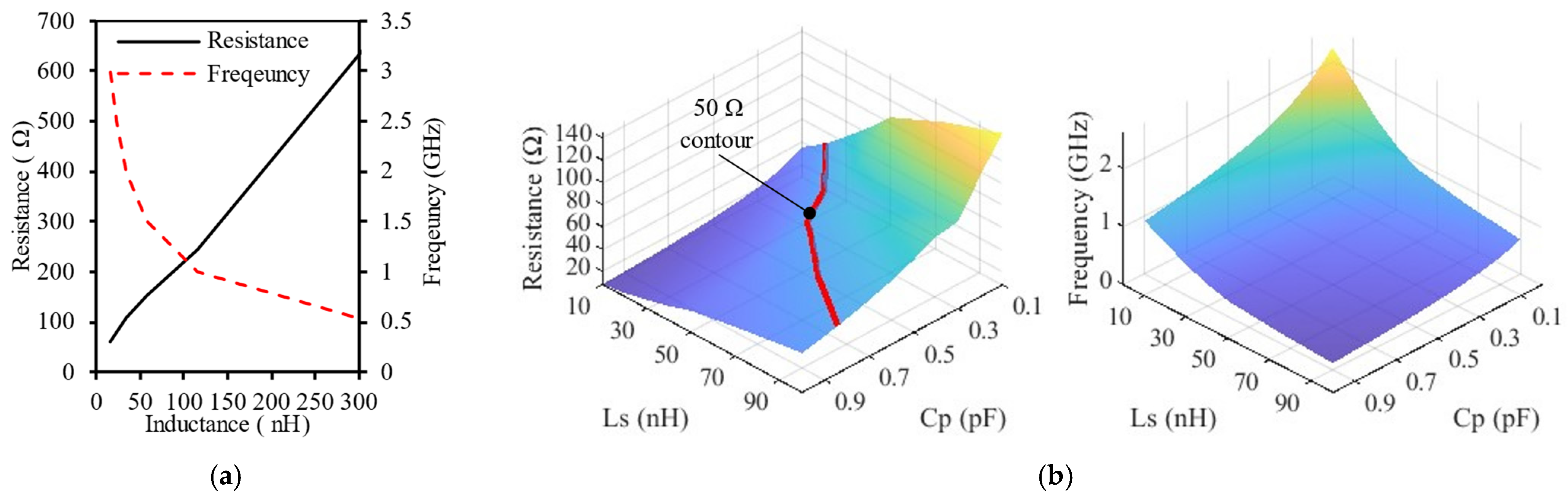
2.1. Analysis

The schematics of the conventional [8] and proposed self-matched rectifier are shown in Figure 1a and Figure 1b, respectively. In both cases, at each frequency band, the self-matched structure consists of a diode and a series inductor. In the proposed case, an additional capacitor is proposed in parallel to the diode to offer comprehensive impedance control. Both designs can achieve a zero-input reactance at an arbitrary frequency of the loading elements. However, as shown in Figure 1c, the input resistance of the conventional self-matched rectifier increases when designed to operate at a lower operating frequency. In the proposed case a 50 Ω matching can be achieved by proper design of the series inductor and capacitor. In Figure 1c, f m a x represents the maximum frequency at which an arbitrary input resistance, R i n , can be designed, 50 Ω in this work, due to the internal capacitance and other intrinsic parameters of the used diode at an available input power level and R L . Figure 1d presents the AC equivalent circuit of the proposed dual-band rectifier, which acts as a two-way diplexer [30] with branch filters implemented as bandpass filters. This configuration facilitates the design of a multi-band rectifier by enabling the addition of parallel branches for multiple frequency bands.
The equivalent circuit of the proposed self-matched rectifier is shown in Figure 2a. The voltage across this self-matched structure can be expressed as (1) where V o , V D P , and V L P are the DC output voltage, the peak voltage across the diode, and the peak voltage across the inductor.
V = V d + V L = V o + V DP cos ω t + V LP cos ω t
The junction voltage varies based on the on/off condition and can be expressed as (2) where V j 0 and V j 1 are the DC component and the peak of the AC component of the junction voltage. V f is the diode’s built-in voltage when the diode state is on. Also, θ is the phase delay between the input voltage and the junction voltage. Following a similar procedure for the on-state of the diode in [8,16], the turn-on angle, o n , should satisfy the condition in (3).
V j = V j 0 + V j 1 cos ω t θ , off   state V f ,                                                                       , on   state
tan o n o n = π R s R L ( 1 + V f / V o )
When the diode is reverse biased the junction resistance, R j , is very high and acts as an open circuit. The typical values of junction capacitance, C j , is a few hundred femto-Farads and of the series resistance, and R s , is a few ohms. Therefore, their corresponding series quality factor, Q s = 1 / ω C j R s , is relatively large. Consequently, the equivalent circuit can be re-drawn as shown in Figure 2b where R P = R s 1 + Q s 2 . Furthermore, the equivalent circuit can be further simplified as shown in Figure 2c considering that R s ¯ , calculated using (4), is the overall series resistance and Q P = ω C j + C p R P is the quality factor of the parallel combination of R P and C j + C p .
R s ¯ = R P 1 + Q P 2 = R s 1 + Q s 2 1 + Q P 2
Furthermore, following a similar analysis for the off state of the diode in [8,16], the input impedance can be expressed as
Z i n = π R s ¯ A + j A 2 + ω 2 B 2 ω L s π R s ¯ ω B A 2 + ω 2 B 2
and
A = o n sin o n cos o n
B = R s ¯ C j + C p π A
At resonance, the reactance in (5) will vanish following the condition:
A 2 + ω 2 B 2 L s = π R s ¯ B
Correspondingly, Z i n will become pure resistive and, by substituting (7) in (5), it can be rewritten as
Z i n = A B × L s = A R s ¯ π A × L s C j + C p
Equation (8) shows that, in the proposed method, the impedance is pure real and can be controlled to an arbitrary value, by proper selection of L s and C p . To elaborate more on this finding, the input resistance and corresponding resonance frequency are designed and plotted against the loading elements for the conventional and proposed method as shown in Figure 3a and Figure 3b, respectively. The SMS7621 diode ( B v = 3 V, V f = 0.51 V, R s = 12 Ω, and C j = 0.1 pF) was utilized in this work. Simulations were performed using the Advanced Design System (ADS).
In the conventional design method, L a value defines the resonance frequency. But it has no control over the value of R i n . The reason behind this can be understood by setting L s = L a and C p = 0 in (8). Consequently, the lower the design resonance frequency, the larger the required value of L a that leads to a larger value of R i n as shown in Figure 3a. Instead, in the proposed design method, the introduction of C p added another degree of freedom. This allowed for the simultaneous design of both the frequency and R i n as shown in Figure 3b.

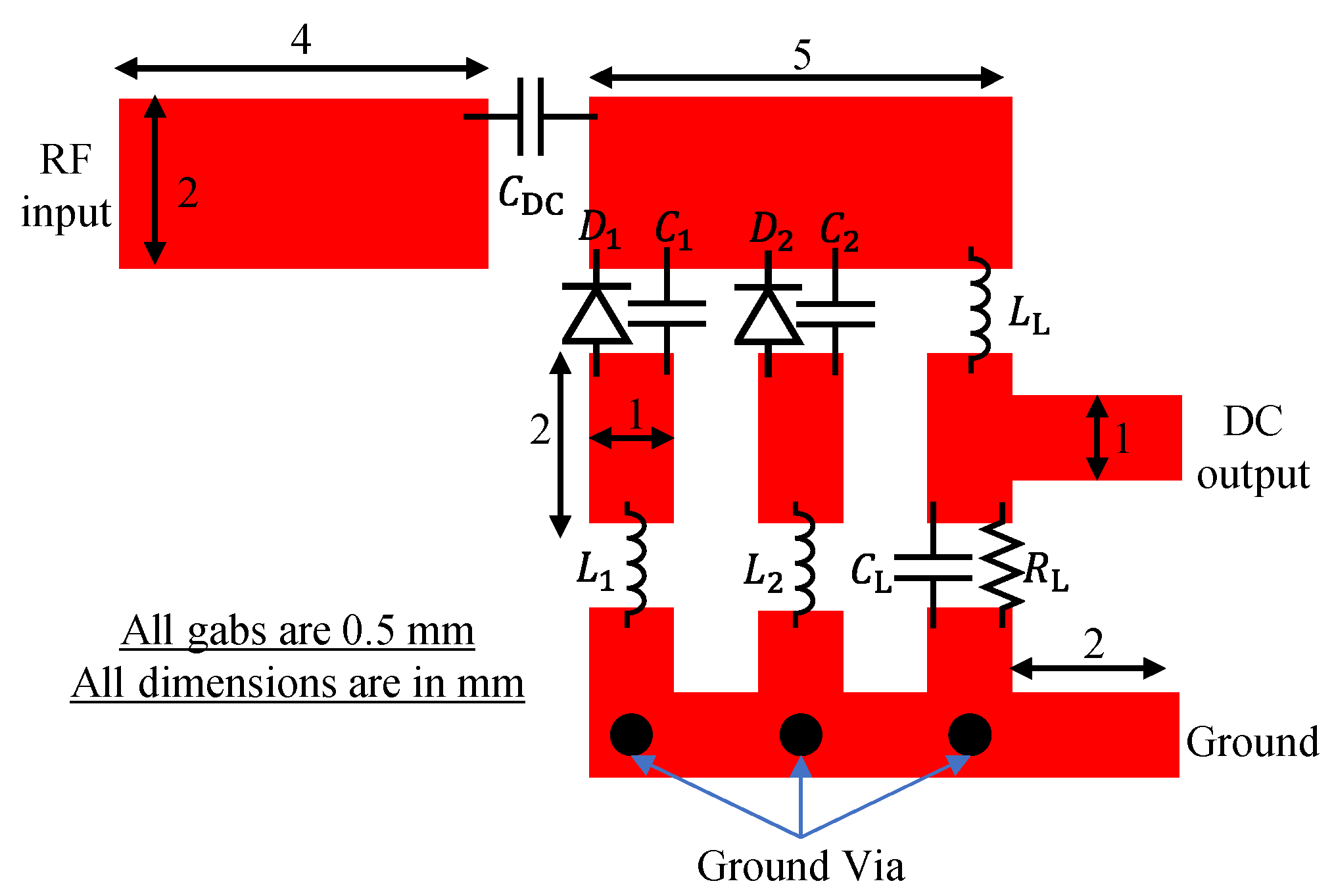
2.2. Design Example of a Dual-Band Rectifier

Based on the analysis in Section 2.1, a dual-band rectifier is designed for operation at 400 MHz and 700 MHz with an assumed DC output load of 2 KΩ. The layout of this proposed dual-band rectifier is shown in Figure 4 and the optimized circuit elements based on (7) and (8) are listed in Table 1.
Rogers RO3003 substrate (height = 0.762 mm, metal thickness = 16 μm, and εr = 3) is used in this design. The simulated reflection coefficient of the proposed dual-band rectifier is shown in Figure 5a at two different input powers. These simulation results confirm that the rectifier is matched at two bands 400 MHz and 700 MHz. The PCE is calculated using (9) where P i n and V L are the input RF power, and the dc output voltage, respectively.
P C E = V L 2 / ( R L P i n )
The effect of the quality (Q) factors of the used inductors is studied when the input power was 0 dBm as shown in Figure 5b. The higher the Q-factor the better the simulated PCE. The PCE is calculated for two different input powers when the Q-factor is 50 as shown in Figure 5c. The PCE is more than 50% for both bands. The Q-factor of 50 represents the approximate value of the Q-factor of the used inductors in Table 1 at these frequency bands.
Furthermore, in Figure 5d, the simulated PCE and output DC voltage are shown versus P i n for both frequency bands. In the first band, at 400 MHz, the simulated PCE is more than 50% from −7 dBm to 10 dBm. In the second band, at 700 MHz, the simulated PCE is more than 50% from −5 dBm to 10 dBm and peaks at about 70% at 7 dBm at both bands. Also, in both cases, for P i n ≥ 0 dBm, a load voltage ≥ 1.06 V is achieved.

3. Fabrication and Measurement Results

3.1. Fabrication and Measurement Setup

The proposed dual-band self-matched rectifier was fabricated on Rogers RO3003 (Tokyo, Japan) based on the design parameters in Table 1. The fabricated dual-band self-matched rectifier is shown in Figure 6. This fabricated dual-band self-matched rectifier has a core area of 0.42 cm2 (7 mm × 6 mm) and an overall area of 0.7 cm2 (7 mm × 10 mm) when the area necessary for connecting the RF connector is included. S-parameters measurements were carried out using the Keysight vector network analyzer (part number: N5222A). Also, PCE measurement was performed using a Keysight analog signal generator (part # E8257D) for RF signal generation, and the output voltage was recorded using a multimeter. Then, the PCE was calculated using (9).

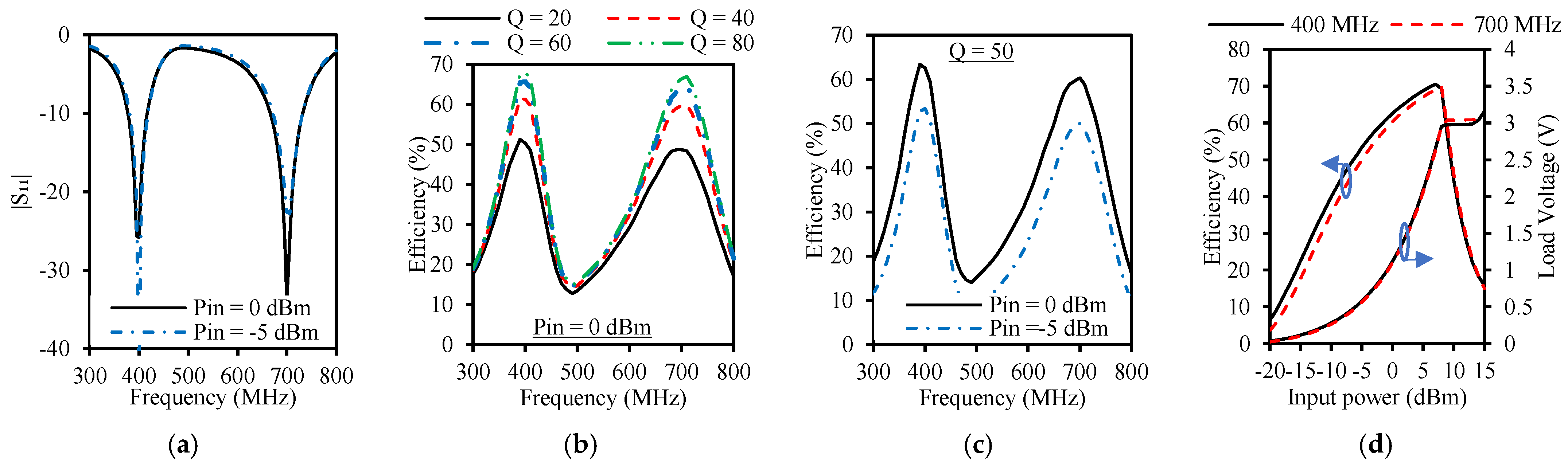
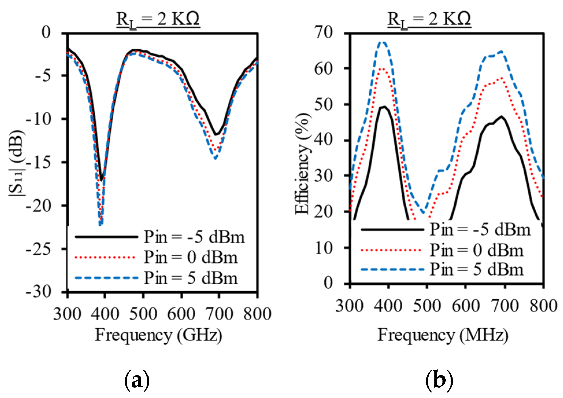
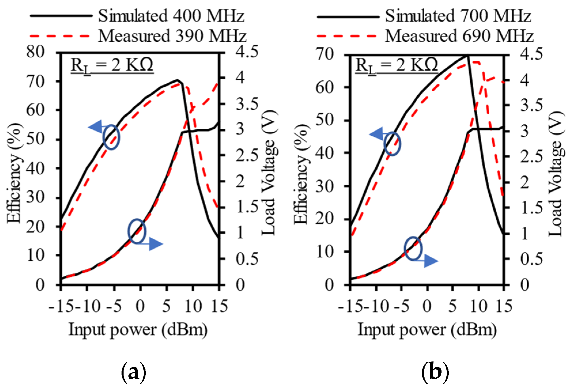
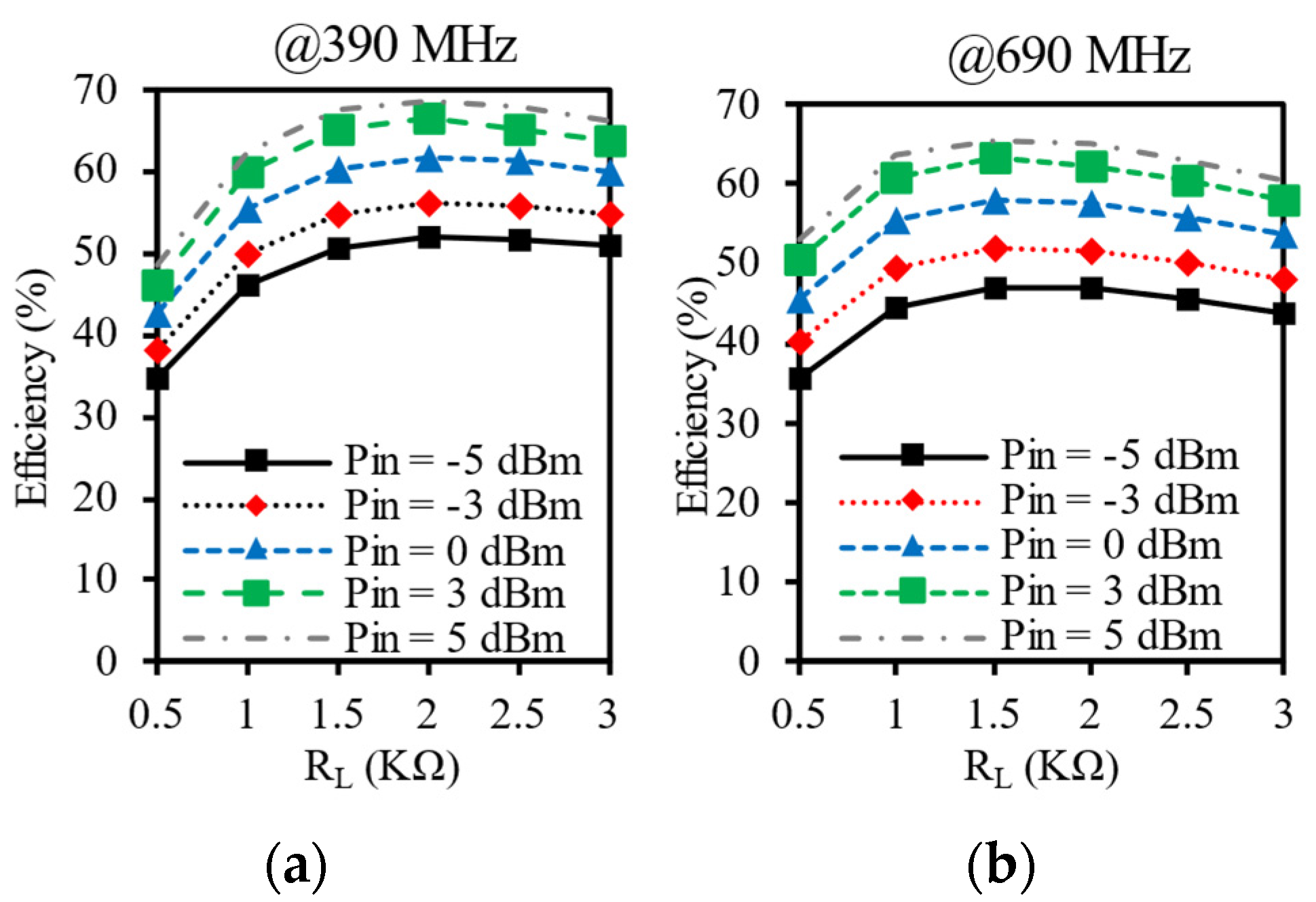
3.2. Measurement Results

The measured |S₁₁| and PCE versus frequency of the fabricated dual-band rectifier at three different input powers and R L = 2 KΩ are shown in Figure 7a and Figure 7b, respectively. The dual-band operation was confirmed at 390 MHz and 690 MHz, which are slightly shifted to lower frequencies than the simulated ones due to the tolerance of the used lumped elements. The PCE varied from 50% to 68% for the 390 MHz band and from 47% to 65% for the 690 MHz band when power changed from −5 to 5 dBm.
Moreover, the simulated and measured PCE versus P i n is compared when R L = 2 KΩ and has a good agreement for both frequency bands as shown in Figure 8. The measured PCE, for the lower frequency band, was more than 50% when input power changed from −5.5 dBm to 11 dBm as shown in Figure 8a. For the upper-frequency band, the measured PCE was more than 50% when the input power ranged from −4 dBm to 12 dBm as shown in Figure 8b.
In addition, the measured PCE versus the output load with different input power powers for the lower and upper bands are shown in Figure 9a and Figure 9b, respectively. In both bands, for an input power of 5 dBm, the measured PCE was more than 50% for 0.5 KΩ < R L < 3 KΩ and more than 62% for 1 KΩ < R L < 3 KΩ. At the lower band, the measured RF-DC conversion efficiencies were more than 46%, 50%, 55.5%, and 60% for input power of −5 dBm, −3 dBm, 0 dBm, and 3 dBm, respectively. Also, at the higher band, the measured RF-DC conversion efficiencies were more than 44.5%, 49.5%, 55.6%, and 60.5% for input powers of −5 dBm, −3 dBm, 0 dBm, and 3 dBm, respectively. These results prove the robustness of the proposed technique against the output dc-load variations.

3.3. Performance Comparison

In Table 2, a detailed comparison with other multi-band rectifiers is provided. A very compact size was achieved despite the low frequency of the implementation. It is 3% the size of the design in [3]. However, this is associated with a slightly lower peak PCE when compared to [3]. The reason is the use of lumped inductors with limited Q-factor. Furthermore, the proposed comprehensive self-matching technique enabled an almost equal peak PCE for both bands. In [8], the peak PCE and the dynamic input power range for PCE > 50% were affected by the level of input resistance which was not exactly 50-Ω at every frequency. Still, our proposed rectifier has an expandability feature like the design in [8]. The dynamic range for PCE > 50% of input power is also comparable to the rectifiers in [3,8] and outperforms the rectifier in [9]. Also, the dynamic range for PCE > 60% of input power outperforms the rectifiers in [8,9].

4. Discussion

The results presented in this study demonstrate the effectiveness and compactness of the proposed dual-band rectifier utilizing self-matched parallel branches. The dual-band operation at 390 MHz and 690 MHz was successfully confirmed through simulation and measurement, with a slight frequency shift due to the tolerance in lumped element values. Despite this shift, the rectifier consistently exhibited high RF-DC PCE, maintaining values over 50% across a wide range of input powers at both bands. The measured PCE for both bands showed significant performance, with peak values reaching 69% at 390 MHz and 68% at 690 MHz, which are comparable to other multi-band rectifiers. The dual-band operation of the rectifier was further validated by a wide dynamic input power range for PCE greater than 50%, with the lower frequency band showing a range from −5 dBm to 11 dBm, and the higher frequency band extending from −4 dBm to 12 dBm. These results are in good agreement with the simulated PCE, further supporting the proposed design’s robustness and reliability in practical applications.
A noteworthy aspect of this work is the proposed self-matching technique, which enables comprehensive impedance control for each rectifier branch. This method not only cancels reactance but also allows for adjustable resistance values, independent of the design frequency. Such flexibility is crucial for ensuring efficient operation across both bands. This approach offers a significant advantage over other methods that control only the reactance, as demonstrated by the improved performance and comparable PCE values in both frequency bands. Furthermore, extending the design to cover additional frequency bands is straightforward by incorporating more parallel branches tuned to the desired operating frequencies. This approach enhances the applicability of the proposed rectifier in diverse WPT scenarios.
The rectifier exhibited stable performance across a wide load range from 0.5 KΩ to 3 KΩ, with PCE remaining above 50% for both bands when the input power was 5 dBm. This characteristic highlights the rectifier’s robustness against load variations, an essential feature for practical deployment in real-world scenarios. The compactness of the design is another key achievement. With a core area of 0.42 cm2, the rectifier offers a significant size reduction compared to previous implementations, such as the design in [3], which is approximately 34 times larger. This compact form factor is particularly beneficial for applications in size-constrained environments, such as integrated circuit designs and wireless energy harvesting systems. While the proposed rectifier outperforms the design in [9] in terms of dynamic range for PCE > 60%, it does show a slightly lower peak PCE compared to [3], due to the use of lumped inductors with limited Q-factor. However, utilizing lumped elements remains an advantageous trade-off for achieving a highly compact design. The proposed self-matching technique also allows for nearly equal peak PCE across both frequency bands, further reinforcing the effectiveness of this approach. Overall, the proposed dual-band rectifier demonstrates promising performance in terms of efficiency, size, and robustness, making it a feasible solution for applications requiring multi-band rectification. Future work can focus on improving the Q-factor of the lumped inductors to enhance the peak PCE further while maintaining the compact design. While the use of lumped inductors introduces a slight reduction in peak PCE, this trade-off enables a significantly more compact design. Alternative implementations using higher-Q inductors, such as wire springs, may enhance efficiency but could compromise integration feasibility and miniaturization. Also, at the low frequencies used in this design, implementing matching networks using printed transmission lines would be impractical due to their large physical size. The required electrical length of quarter-wavelength sections at 400 MHz and 700 MHz would result in prohibitively large structures, making them unsuitable for compact circuit implementations.
Additionally, future implementations of the proposed rectifier could involve integration with an antenna in a complete WPT setup. This would allow for a more comprehensive evaluation of system-level performance, considering factors such as impedance matching, radiation efficiency, and environmental effects. However, achieving optimal integration requires careful design trade-offs to maintain efficiency and minimize losses. Exploring these aspects in future work could further enhance the rectifier’s practical feasibility for real-world applications.

5. Conclusions

This work presented a compact and efficient dual-band rectifier with self-matched branches. Regardless of the design frequency, comprehensive impedance control was achievable for each branch without affecting the other. The impedance of the self-matched branch was analyzed, and design equations were derived. We demonstrated that this approach provides effective impedance matching for each branch by canceling reactance while allowing for adjustable resistance values. As a proof-of-concept, a dual-band rectifier was fabricated for verification, featuring a core area of 0.42 cm2 and an overall area of 0.7 cm2 including the RF connector. Measurements confirmed the dual-band operation at 390 MHz and 690 MHz with more than 60% of PCE for input power ranges from 0 to 10 dBm and 1 to 11 dBm, respectively.
While this work focused on sub-GHz frequencies, the proposed self-matching approach can be extended to higher-frequency designs, where distributed transmission lines could replace lumped components to further enhance integration. At GHz-range operation, careful consideration of parasitic effects and component selection would be required to maintain impedance matching and efficiency. Future work may explore these extensions and investigate alternative design techniques for multi-band rectification at higher frequencies.

Author Contributions

Conceptualization, A.B.; methodology, A.B.; software, A.B., W.J. and R.K.P.; validation, A.B. and W.J.; formal analysis, A.B.; investigation, A.B. and W.J.; resources, R.K.P.; data curation, A.B. and W.J.; writing—original draft preparation, A.B.; writing—review and editing, A.B., W.J. and R.K.P.; visualization, A.B. and W.J.; funding acquisition, A.B. and R.K.P.; supervision, A.B. and R.K.P. All authors have read and agreed to the published version of the manuscript.

Funding

This research was supported in part by the Japan Society for the Promotion of Science (JSPS) KAKENHI under Grant 22K14260, and in part by the activities of VLSI Design and Education Center (VDEC), The University of Tokyo, in collaboration with Keysight Technologies Japan, Ltd.

Data Availability Statement

Data are contained within the article.

Conflicts of Interest

The authors declare no conflicts of interest.

Abbreviations

The following abbreviations are used in this manuscript:
WPTWireless Power Transfer
IoTInternet of Things
PCEPower Conversion Efficiency
BWBandwidth
ADSAdvanced Design System
Q-factorQuality Factor

References

  1. Deng, X.; Yang, P.; Chen, S.; Ren, W. Design of a 2.4 & 5.8 GHz Efficient Circularly Polarized Rectenna for Wireless Power Transfer Applications. Electronics 2023, 12, 2645. [Google Scholar] [CrossRef]
  2. Mansour, M.M.; Torigoe, S.; Yamamoto, S.; Kanaya, H. Compact and Simple High-Efficient Dual-Band RF-DC Rectifier for Wireless Electromagnetic Energy Harvesting. Electronics 2021, 10, 1764. [Google Scholar] [CrossRef]
  3. Nam, H.; Bui, G.T.; Nguyen, D.A.; Seo, C. A Compact and High-Efficiency 0.915/2.45/5.8 GHz Triple-Band Rectifier with Harmonic Suppression Based on Coupled Transmission Line. IEEE Trans. Circuits Syst. II Express Briefs 2024, 71, 3553–3557. [Google Scholar] [CrossRef]
  4. Woo, K.; Bui, G.T.; Nguyen, D.A.; Seo, C. A Compact and High-Efficiency Design of Triple-Band Rectifier with Harmonic Suppression for Wireless Power Transfer. IEEE Microw. Wirel. Technol. Lett. 2024, 34, 111–114. [Google Scholar] [CrossRef]
  5. Du, C.H.; Cheng, F.; Gu, C. Efficient Tri-Band Rectifier Using Multistub Matching Network for WPT Applications. IEEE Microw. Wirel. Technol. Lett. 2023, 33, 1361–1364. [Google Scholar] [CrossRef]
  6. Yue, Z.; Xu, X.; Li, S.; Zhu, Y.H.; Lin, X.Q. Efficient and Compact Tri-Band Rectifier with Large Frequency Ratio for WPT. IEEE Microw. Wirel. Compon. Lett. 2022, 32, 1355–1358. [Google Scholar] [CrossRef]
  7. Tafekirt, H.; Pelegri-Sebastia, J.; Bouajaj, A.; Reda, B.M. A Sensitive Triple-Band Rectifier for Energy Harvesting Applications. IEEE Access 2020, 8, 73659–73664. [Google Scholar] [CrossRef]
  8. Wang, S.H.; Zheng, S.Y.; Leung, K.W.; Xia, M.H. A Self-Matched Multi-Band Rectifier for Efficient Electromagnetic Energy Harvesting. IEEE Trans. Circuits Syst. I Regul. Pap. 2021, 68, 4556–4565. [Google Scholar] [CrossRef]
  9. Liu, J.; Huang, M.; Du, Z. Design of Compact Dual-Band RF Rectifiers for Wireless Power Transfer and Energy Harvesting. IEEE Access 2020, 8, 184901–184908. [Google Scholar] [CrossRef]
  10. Shen, S.; Zhang, Y.; Chiu, C.Y.; Murch, R. A Triple-Band High-Gain Multibeam Ambient Rf Energy Harvesting System Utilizing Hybrid Combining. IEEE Trans. Ind. Electron. 2020, 67, 9215–9226. [Google Scholar] [CrossRef]
  11. Song, C.; Huang, Y.; Zhou, J.; Carter, P.; Yuan, S.; Xu, Q.; Fei, Z. Matching Network Elimination in Broadband Rectennas for High-Efficiency Wireless Power Transfer and Energy Harvesting. IEEE Trans. Ind. Electron. 2017, 64, 3950–3961. [Google Scholar] [CrossRef]
  12. Liu, J.; Zhang, X.Y.; Yang, C.L. Analysis and Design of Dual-Band Rectifier Using Novel Matching Network. IEEE Trans. Circuits Syst. II Express Briefs 2018, 65, 431–435. [Google Scholar] [CrossRef]
  13. Song, C.; Huang, Y.; Carter, P.; Zhou, J.; Yuan, S.; Xu, Q.; Kod, M. A Novel Six-Band Dual CP Rectenna Using Improved Impedance Matching Technique for Ambient RF Energy Harvesting. IEEE Trans. Antennas Propag. 2016, 64, 3160–3171. [Google Scholar] [CrossRef]
  14. Bougas, I.D.; Papadopoulou, M.S.; Boursianis, A.D.; Nikolaidis, S.; Goudos, S.K. Dual-Band Rectifier Circuit Design for IoT Communication in 5G Systems. Technologies 2023, 11, 34. [Google Scholar] [CrossRef]
  15. Liu, Y.; Xie, G. A Compact Broadband Rectifier Based on Coupled Transmission Line for Wireless Power Transfer. Electronics 2024, 13, 3901. [Google Scholar] [CrossRef]
  16. Gyawali, B.; Aboualalaa, M.; Barakat, A.; Pokharel, R.K. Design of Miniaturized Sub-6 GHz Rectifier with Self-Impedance Matching Technique. IEEE Trans. Circuits Syst. I Regul. Pap. 2024, 71, 3413–3422. [Google Scholar] [CrossRef]
  17. Xiao, Y.Y.; Ou, J.H.; Bo, S.F.; Che, W.; Zhang, X.Y. A Simple Technology for Designing Ultrawideband Rectifiers. IEEE Trans. Microw. Theory Tech. 2024, 72, 1424–1432. [Google Scholar] [CrossRef]
  18. Yu, S.; Cheng, F.; Gu, C.; Wang, C.; Huang, K. Compact and Efficient Broadband Rectifier Using T-Type Matching Network. IEEE Microw. Wirel. Compon. Lett. 2022, 32, 587–590. [Google Scholar] [CrossRef]
  19. Gyawali, B.; Thapa, S.K.; Barakat, A.; Yoshitomi, K.; Pokharel, R.K. Analysis and Design of Diode Physical Limit Bandwidth Efficient Rectification Circuit for Maximum Flat Efficiency, Wide Impedance, and Efficiency Bandwidths. Sci. Rep. 2021, 11, 19941. [Google Scholar] [CrossRef] [PubMed]
  20. Liu, W.; Huang, K.; Wang, T.; Zhang, Z.; Hou, J. A Broadband High-Efficiency RF Rectifier for Ambient RF Energy Harvesting. IEEE Microw. Wirel. Compon. Lett. 2020, 30, 1185–1188. [Google Scholar] [CrossRef]
  21. He, Z.; Liu, C. A Compact High-Efficiency Broadband Rectifier with a Wide Dynamic Range of Input Power for Energy Harvesting. IEEE Microw. Wirel. Compon. Lett. 2020, 30, 433–436. [Google Scholar] [CrossRef]
  22. Wu, P.; Huang, S.Y.; Zhou, W.; Yu, W.; Liu, Z.; Chen, X.; Liu, C. Compact High-Efficiency Broadband Rectifier with Multi-Stage-Transmission-Line Matching. IEEE Trans. Circuits Syst. II Express Briefs 2019, 66, 1316–1320. [Google Scholar] [CrossRef]
  23. Zheng, S.; Liu, W.; Pan, Y. Design of an Ultra-Wideband High-Efficiency Rectifier for Wireless Power Transmission and Harvesting Applications. IEEE Trans Ind. Inf. 2019, 15, 3334–3342. [Google Scholar] [CrossRef]
  24. Huang, M.; Lin, Y.L.; Ou, J.H.; Zhang, X.Y.; Lin, Q.W.; Che, W.; Xue, Q. Single-and Dual-Band Rf Rectifiers with Extended Input Power Range Using Automatic Impedance Transforming. IEEE Trans. Microw. Theory Tech. 2019, 67, 1974–1984. [Google Scholar] [CrossRef]
  25. Wu, P.; Huang, S.Y.; Zhou, W.; Liu, C. One Octave Bandwidth Rectifier with a Frequency Selective Diode Array. IEEE Microw. Wirel. Compon. Lett. 2018, 28, 1008–1010. [Google Scholar] [CrossRef]
  26. Lin, Y.L.; Zhang, X.Y.; Du, Z.X.; Lin, Q.W. High-Efficiency Microwave Rectifier with Extended Operating Bandwidth. IEEE Trans. Circuits Syst. II Express Briefs 2018, 65, 819–823. [Google Scholar] [CrossRef]
  27. Mansour, M.M.; Kanaya, H. Compact and Broadband RF Rectifier with 1.5 Octave Bandwidth Based on a Simple Pair of L-Section Matching Network. IEEE Microw. Wirel. Compon. Lett. 2018, 28, 335–337. [Google Scholar] [CrossRef]
  28. DeLong, B.J.; Kiourti, A.; Volakis, J.L. A Radiating Near-Field Patch Rectenna for Wireless Power Transfer to Medical Implants at 2.4 GHz. IEEE J. Electromagn. RF Microw. Med. Biol. 2018, 2, 64–69. [Google Scholar] [CrossRef]
  29. Jordan, W.; Barakat, A.; Gyawali, B.; Pokharel, R.K. High-Efficiency Platinum-Band CMOS Rectifier Using Modified Body-Biasing Technique. IEEE Microw. Wirel. Technol. Lett. 2024, 34, 1290–1292. [Google Scholar] [CrossRef]
  30. Gao, L.; Lin, T.W.; Rebeiz, G.M. Design of Tunable Multi-Pole Multi-Zero Bandpass Filters and Diplexer with High Selectivity and Isolation. IEEE Trans. Circuits Syst. I Regul. Pap. 2019, 66, 3831–3842. [Google Scholar] [CrossRef]
Figure 1. Multi-band rectifier with self-matched branches: (a) conventional structure [8]; (b) proposed structure; (c) comparison between input resistance, R i n , in both cases where f m a x represents the maximum frequency at which a specified R i n can be achieved; (d) AC equivalent circuit of dual-band rectifier.
Electronics 14 00933 g001
Figure 2. Equivalent circuit of the proposed self-matched rectifier: (a) initial circuit; (b) circuit at off-state condition; (c) final circuit at off-state condition.
Electronics 14 00933 g002
Figure 3. Input resistance, R i n , and frequency of the self-matched branch versus the loading elements when P i n = 0 dBm for the conventional ( L a ) and proposed ( L s and C p ) cases. In conventional design, diode characteristics as well as the loading determines R i n . In the proposed design case, an arbitrary resistance can be achieved by proper loading. In both cases, the input reactance is zero achieving self-matching: (a) conventional; (b) proposed.
Electronics 14 00933 g003
Figure 4. Layout of the proposed dual-band self-matched rectifier.
Electronics 14 00933 g004
Figure 5. ADS simulation results of the proposed dual-band self-matched rectifier: (a) reflection coefficient (|S₁₁|); (b) RF-DC PCE varying Q-factor of the inductors at P i n = 0 dBm; (c) PCE varying P i n for Q = 50; (d) PCE and DC load voltage versus input power assuming inductors have a Q-factor of 50.
Electronics 14 00933 g005
Figure 6. Photo of the fabricated dual-band rectifier.
Electronics 14 00933 g006
Figure 7. Measurement results of the proposed dual-band rectifier versus frequency: (a) |S₁₁|; (b) PCE.
Electronics 14 00933 g007
Figure 8. Comparison between simulated and measured results versus input power: (a) lower-frequency band; (b) upper-frequency band.
Electronics 14 00933 g008
Figure 9. Measured PCE at different input power levels versus load resistance: (a) lower-frequency band; (b) upper-frequency band.
Electronics 14 00933 g009
Table 1. Optimized elements of the designed dual-band rectifier.
ElementValueUnitPart Number
D 1 ,   D 2 --SMS7621-079LF
C D C 56pFGQM1875C2E560FB12
L 1 82nHLQW15AW82NG80
L 2 36nHLQW15AN36NG8Z
C 1 1.3pFGJM1555C1H1R3WB01
C 2 0.8pFGJM1555C1HR80WB01D
L L 120nHLQW15ANR12J00
C L 56pFGQM1875C2E560FB12
R L 2-
Table 2. Performance summary of the proposed rectifier and comparison with state-of-the-art multi-band rectifiers.
ReferenceBandsFrequency
(GHz)
P C E m a x (%) @ P i n (dBm) Dynamic P i n Range (dBm) * DiodeSize (cm2)
PCE > 50%PCE > 60%
This work20.3969 @ 8 dBm−5.5 to 110 to 10SMS76210.42
0.6968 @ 8.5 dBm−4 to 12 1 to 11
[3]30.89579.9 @ 9.5 dBm−5 to 13.5−1.5 to 12.5BAT15-03W15
2.3874.6 @ 11 dBm−3.5 to 130.5 to 12.5
5.5773.6 @ 13.5 dBm1.5 to 165 to 15.5
[8]22.38 67.7 @ 5 dBm−7 to 11−2 to 9BAT15-03WNR
4.9955.3 @ 5 dBm−2.5 to 9NA
31.78 60.9 @ 5 dBm−5 to 82.5 to 6
2.3571.4 @ 5 dBm−7 to 10−3 to 8.5
4.9754 @ 5 dBm0 to 7NA
[9]20.91569.2 @ −1 dBm−11.8 to 2.5−6 to 1.5SMS763018.8
2.4564.1 @ −1 dBm−8.6 to 1.7−4 to −0.5
* Extracted from curves, NA = Not Applicable, NR = Not reported.
Disclaimer/Publisher’s Note: The statements, opinions and data contained in all publications are solely those of the individual author(s) and contributor(s) and not of MDPI and/or the editor(s). MDPI and/or the editor(s) disclaim responsibility for any injury to people or property resulting from any ideas, methods, instructions or products referred to in the content.

