Abstract
Enhancing power density is a primary objective in electronic power converters. This can be accomplished by employing smaller inductors operating in partial magnetic saturation. In this study, an embedded digital controller is proposed, based on nonlinear model predictive control (NMPC), for the regulation of a DC–DC boost converter, exploiting a partially saturating inductor. The NMPC prediction model exploits a behavioral inductor model that accounts for magnetic saturation and losses and allows the converter regulation while enforcing constraints. The NMPC controller is implemented on a field programmable gate array (FPGA), demonstrating its real-time feasibility while successfully controlling a boost converter operating at switching frequencies up to 80 kHz. Hardware–software co-simulation results show accurate voltage regulation and constraint satisfaction, even under partial magnetic saturation.
1. Introduction
The magnetic saturation of inductor cores leads to a reduction in the material’s permeability as the magnetic field within the core increases. From the perspective of the inductor, this results in a decrease in inductance as current increases—either gradually (as in iron powder core inductors) or abruptly (as in ferrite core inductors). Research has demonstrated that utilizing partially saturated inductors can enhance the power density of power converters, albeit with a slight increase in power loss. The groundbreaking work in [1] illustrates how inductor saturation can be managed in power converters with minimal impact on power consumption. Further studies, including [2,3], provide a more detailed analysis, also considering temperature effects [4].
Designing, simulating, and controlling power converters with partially saturating inductors requires accurate models to predict their operational behavior. Several nonlinear behavioral inductor models are reviewed in [5,6,7]. The range of validity of these models has been extended in [8,9,10] where inductance and power losses are reproduced for different operating frequencies, applied waveforms, air-gap lengths, and core materials.
Model predictive control (MPC), which can be easily implemented on digital circuits [11], is frequently applied to power converters [12,13], offering superior performance compared to traditional model-free proportional–integral (PI) regulators. MPC allows enforcing input and state constraints, particularly important for current limitations (for safety reasons) in power converters. Applications include four-switch, three-phase rectifiers in balanced grids [14] and inverters in unbalanced grids [15,16]. For boost converters, linear MPC is applied in [17], and nonlinear MPC (NMPC) in [18].
Despite these advancements, few implementations consider nonlinear inductance. Various nonlinearities, including magnetic saturation, are addressed in [19], where the inductance of a powder iron core inductor is modeled using an exponential function, and the MPC problem is solved with a fast gradient algorithm, which does not allow imposing current constraints. For ferrite core inductors, ref. [20] introduces an explicit linear MPC controller for a buck converter, relying on a simplified inductor model with step-like inductance and no losses.
In a previous study [21], we exploited nonlinear MPC for the voltage regulation of a DC–DC boost converter by imposing current constraints and using a ferrite core inductor model [9], which represents inductance as an arctangent function of current while accounting for instantaneous losses. This model provides significantly greater accuracy than the simplified approach in [20]. The main limitation of [21] is that only simulation results are proposed, without checking if the technique can be applied to a power converter in real time.
The main novelty of this paper is the FPGA implementation of the technique proposed in [21], which relies on a nonlinear inductor model, for obtaining an embedded real-time controller. This requires the use of limited hardware resources with tight constraints on the circuit latency. Proper algorithms should be therefore adopted for both the nonlinear programming and the numerical integration of the system for prediction. Moreover, fixed-point data representation is mandatory to fulfill real-time constraints.
Several FPGA-based linear MPC implementations are surveyed in [22]. Concerning NMPC on FPGA, different algorithms have been applied, including particle swarm optimization [23,24], mesh adaptive direct search (MADS) [25], and gradient-based techniques [26,27,28]. To perform the optimizations required by the NMPC approach, we chose the MADS algorithm, a zero-order method that does not require the evaluation of derivatives of the cost function. As shown in [25,29,30], it is particularly suitable for microcontroller and FPGA implementations, especially for small-size problems, as considered in this work. Other optimization algorithms suitable for FPGA implementation could be exploited [23,24,26,27,28], possibly leading to lower latency and/or resource occupation. However, MADS proved to be successfully applicable, and comparing different optimization techniques in FPGA is out of the scope of this work. To the authors’ knowledge, a digital circuit for real-time control of a power converter that exploits a nonlinear inductor model for prediction is not available in the literature yet. The performances of the proposed circuit are validated through hardware–software co-simulations.
2. Materials and Methods
2.1. Boost Converter Model
We consider the DC–DC boost converter, whose circuit model is shown in Figure 1.
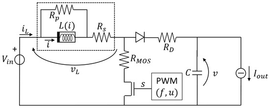
Figure 1.
Circuit model of the boost converter.
A pulse width modulation (PWM) signal s with frequency f (period ) and duty cycle u is applied to the gate of a MOS transistor that behaves like a switch: when the MOS conducts current (ON phase), through a resistance that models the conduction losses; when the transistor is an open circuit and the current flows through the diode, with forward voltage drop and conduction resistance . A load is represented as a variable current source , whereas the inductor (enclosed in a dashed rectangle) is modeled through a nonlinear lossless inductor (with differential inductance , flux linkage , and current i) and two resistors ( and ), accounting for all power losses [21]. We are interested in controlling the converter also when the inductor operates in partial saturation, where the differential inductance drops as the current increases:
where parameters , , , , , and I are identified starting from experimental measurements of and . Specifically, a subset of these measurements is used for model identification, where the model parameters are determined by solving a nonlinear optimization problem. Another subset of the measurements is used for model validation to assess the accuracy of the identified parameters. All details regarding the measurement process, parameter identification, and validation methodology can be found in [21]. Once the model parameters have been identified, by assuming that the current i can be computed as , the flux linkage in the lossless inductor can be evaluated as a function of the current i as
Even if an analytical expression is available for , its evaluation is time- and resource-consuming for an embedded implementation on FPGA. Therefore, 14 couples , are stored in a look-up table (LUT), and functions and are computed through linear interpolation.
Because of the fixed-point embedded implementation of the controller, it is convenient to refer to normalized dimensionless quantities. Therefore, we define , , , , , , . Coefficients , , and are set so that the normalized variables never exceed 1 during the converter operation.
Unlike [21], where i was considered a state variable, here we set the system state as . The input is u, whereas the vector of measurable parameters is . According to these choices, the continuous-time normalized equations of the boost converter (see Appendix A for the details) are:
and the normalized current is
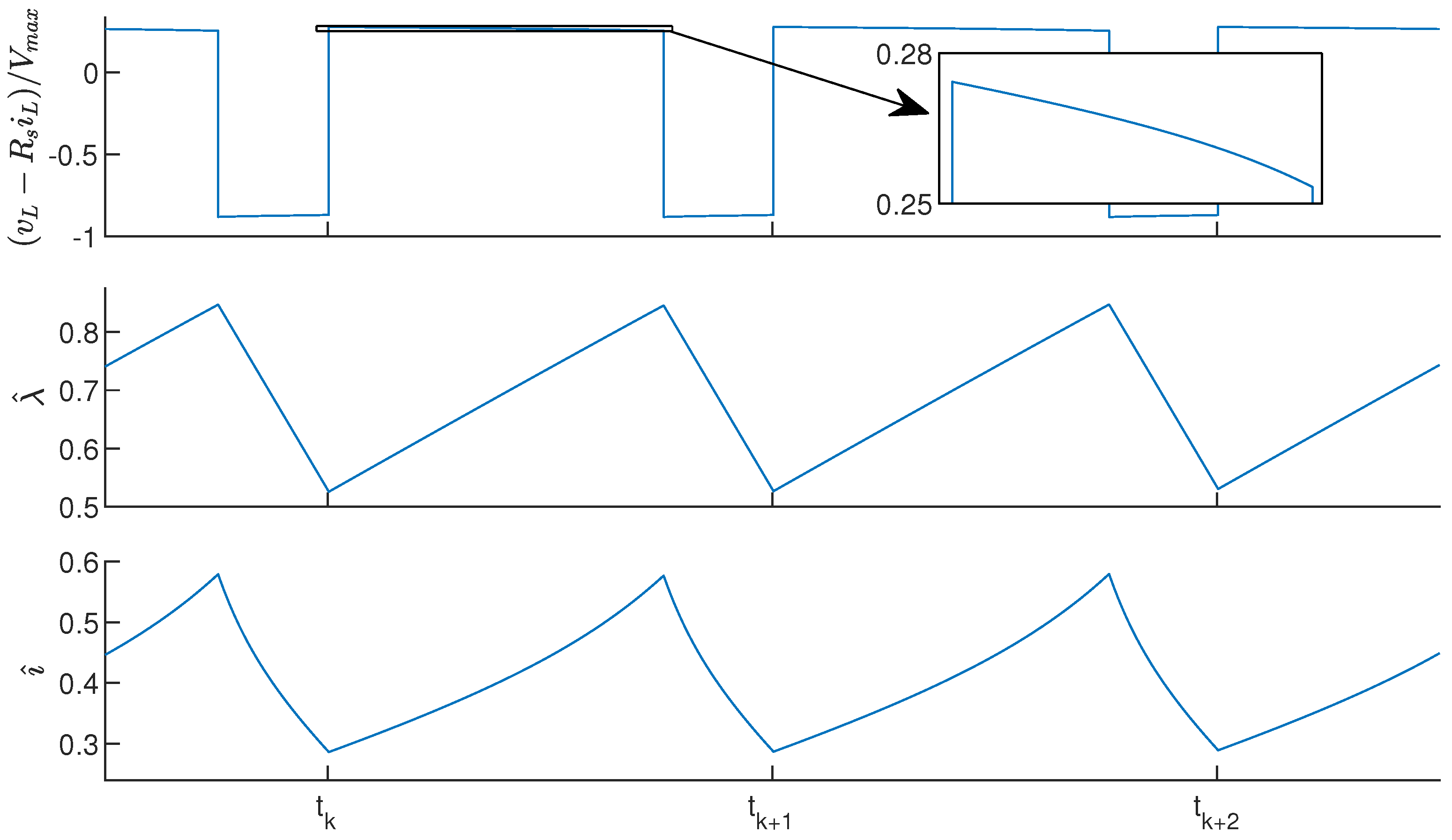
Figure 2 shows time plots of the normalized voltage across the lossless inductor (upper panel), (middle panel), and (lower panel) at steady state. The curves have been obtained by simulating the boost converter model of Figure 1 with the parameters specified in Section 3 using Simulink and the Simscape Electrical library. The k-th PWM period starts at time , when s switches from 0 to 1, and ends at time . The duty cycle is assumed to be piecewise constant, with value in the k-th period (). If losses were neglected, the inductor voltage would be a square wave, and the flux linkage would be its integral over time, resulting in a triangular wave. The presence of losses introduces small distortions in both curves. By contrast, current i may be strongly distorted when the inductor operates in partial saturation, due to the nonlinear behavior of the inductance, as shown in the bottom panel.
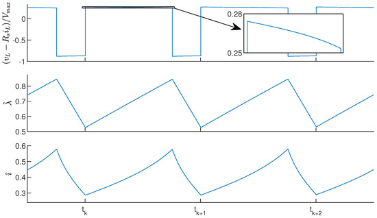
Figure 2.
Time plots of the normalized lossless inductor voltage (top panel), flux linkage (middle panel), and current (bottom panel).
2.2. Nonlinear MPC
The aim of the NMPC controller is to keep the average (over a period) output voltage v to a reference value , while satisfying constraints on the duty cycle and on the inductor current [21], namely and . The distance between the normalized reference voltage and the average (within the k-th PWM period) output voltage is defined as . We also define .
With NMPC, a nonlinear constrained optimization problem must be solved at each PWM period. The cost function to minimize is computed based on a prediction of the system states over a prediction horizon N. The inputs are optimized up to a control horizon . Many algorithms are available for nonlinear optimization. Among them, zero-order methods (not requiring the evaluation of derivatives) are the most suitable for an embedded implementation. Here we exploit the MADS algorithm, adapted for a digital implementation [25]. This MADS implementation only requires performing operations whose computation is efficient with fixed-point hardware architectures: sums/subtractions, multiplications, shifts, rounding operations, and comparisons. Of course, the computational complexity and latency of the overall optimization algorithm strongly depend on functions F and G (see Equations (3) and (4)), which are evaluated several times at each algorithm iteration.
At time , we use as inputs the measurements of , , , , the optimal input predicted by the MPC at the previous step, and the reference voltage . This means that we assume that p remains constant within the interval of the prediction horizon. At the beginning, . Current can be computed by rearranging Equation (4),
Therefore, . The optimization variables are gathered in a vector .
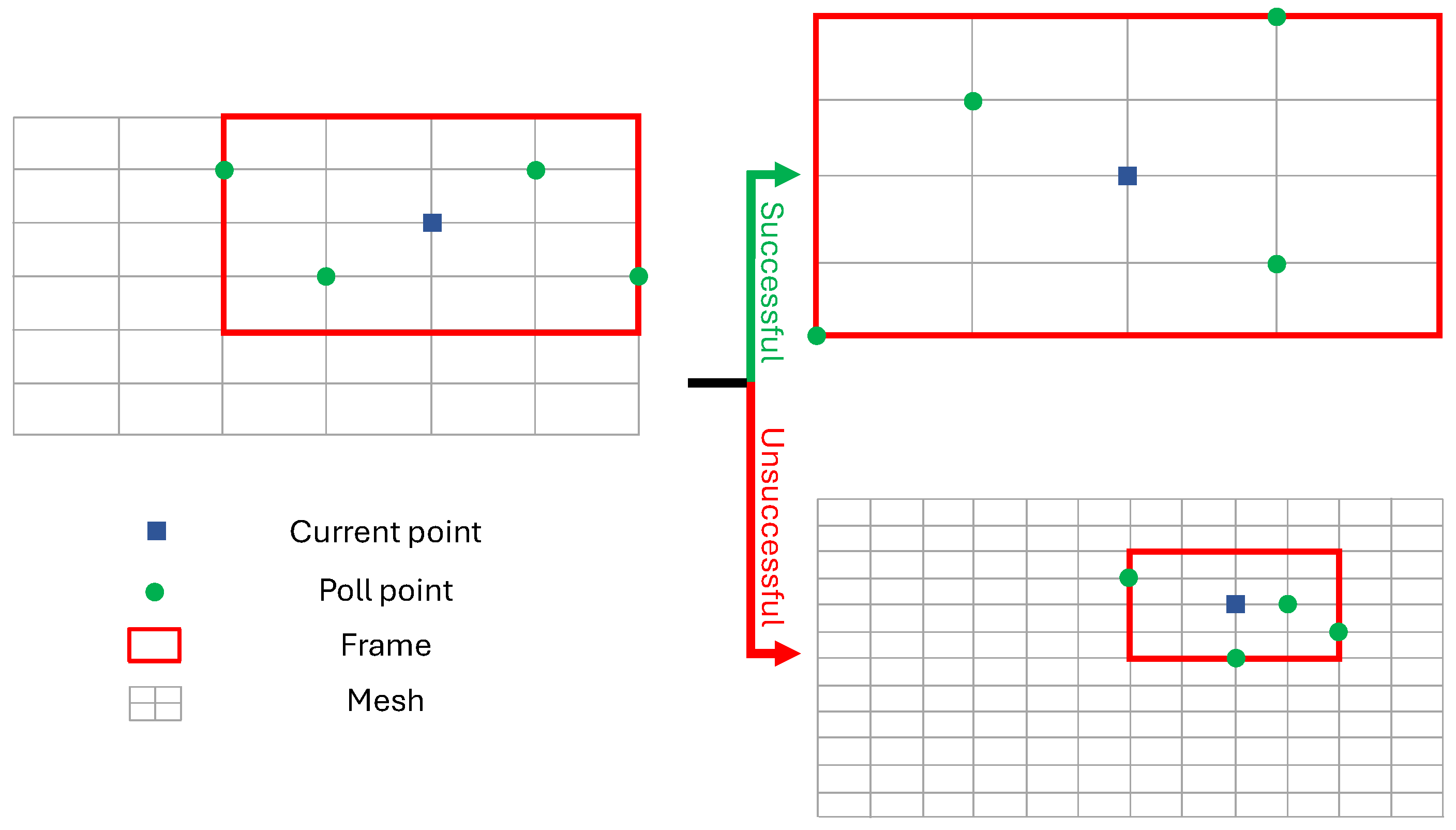
The MADS algorithm is run for iterations. The reader is referred to [25] and references therein for a detailed explanation of the MADS algorithm. A summary, for ease of reference, is reported in the following. At each iteration, poll vectors , , are generated, containing entries within bounds and . The poll vectors lie on a mesh, inside a frame [31] (see Figure 3). Each poll vector contains the system inputs within the control horizon, i.e., . The remaining inputs, up to the prediction horizon, are set as . The input sequence can be applied for the integration of system (3), thus obtaining , , and (through Equation (4)) up to the prediction horizon. For control purposes, only the values of and at the PWM switching times are relevant. After computing terms and , the following cost function J can be evaluated, which penalizes both deviations of from its reference value and fast variations of u:

Figure 3.
Example of a MADS iteration with 3.
Since a progressive barrier approach [32] is exploited, a constraint violation function V must also be computed that is equal to 0 when the current is within and , and grows when the current exceeds the constraints:
Here, is the set of all switching instants within the prediction horizon.
After evaluating all poll points, based on the cost and violation functions, the MADS iteration can be declared successful or not. In the first case, the frame is enlarged and the mesh becomes coarser. In the second case, the opposite happens. A graphical representation (with 3) of a MADS iteration is shown in Figure 3.
At the end of the optimization, after iterations, an optimal solution
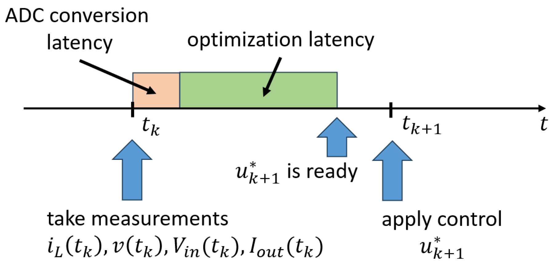
is obtained. Input is applied to the converter at time . A new optimization problem is solved through MADS at time in a receding horizon fashion, by using as a starting input. A timeline of the controller’s operation is shown in Figure 4: analog measurements are acquired at time and converted to digital signals with a certain latency (orange rectangle). The optimization problem is then solved (the latency is indicated with the green rectangle) leading to optimal control , which is then applied at time . This is different from what was done in [21], where the latency was neglected and the output of the optimization at time was , applied instantaneously to the boost at time . We remark that the total latency does not affect the control performance, provided that it remains lower than the system sampling time.
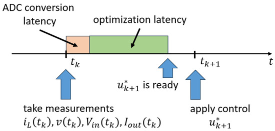
Figure 4.
Timeline of the controller’s operation.
2.3. Numerical Integration of the Model
In [21], system (3) was solved through the ode45 MATLAB R2023b function, with high accuracy. For a real-time embedded implementation, where the execution time is a major constraint, we have to find an alternative solution.
Consider a generic nonlinear dynamical system . The explicit midpoint method [33] estimates the state at time as
This requires the evaluation of function at two different points.
We applied the midpoint method to the boost converter with . In our case, the function is the function defined in Equation (3), under the assumption that both u and p are constant within a period, which is consistent with the discussion presented in Section 2.2. Four function evaluations are necessary within a PWM period. For comparison purposes, we exploit both Equations (3), with as a state variable, and the equations used in [21], where the state variable was . Figure 5 shows voltage (top panel) and current (bottom panel) obtained with ode45 (black curves) and with midpoint methods by exploiting flux linkage and current as state variables (see legend). The integration diverges if state is used, but good accuracy is obtained with state variable . This is because, as shown in Figure 2, the flux linkage is approximately a triangular wave, whereas the current has a cusp-like behavior. Therefore, within two consecutive integration instants, is approximately constant, unlike . This is the reason why we chose as a state variable instead of as in [21]. Better performance is obtained using more points, at the cost of a higher computation time. The implementation of the midpoint method for the boost converter is detailed in Appendix B.
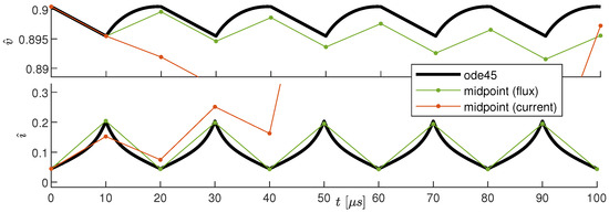
Figure 5.
Comparison of ode45 integration, midpoint integration with flux linkage as a state variable, and midpoint integration with current as a state variable.
For solving the optimization problem, the evaluation of the cost function J is the most computationally expensive task, due to numerical integration. Using the midpoint method, the most demanding operation is computing F. The FPGA hardware resources and control algorithm latency strongly depend on the control horizon N, the prediction horizon , and the number of MADS iterations . At each iteration, MADS evaluates the cost function at poll points (see Figure 3), and F is computed times for each call to the cost function. In summary, at each sampling time, calls to the function F are required, where
These parameters also affect the control performance, as detailed in the following sections.
2.4. FPGA Implementation
The control algorithm is described in C language through AMD Vitis HLS 2024.2, a high-level synthesis (HLS) tool [34,35], which converts an algorithm coded in C into a fully timed hardware implementation. The workflow consists of the following standard key steps:
- Compilation;
- C simulation through a testbench;
- Register–transfer level (RTL) generation, where the C code is translated into an RTL description, by scheduling operations, binding resources, extracting control logic, and defining external communication;
- RTL synthesis, which converts the RTL description into a gate-level netlist;
- RTL simulation through a testbench;
- Implementation, where the netlist is placed and routed onto device resources, within the logical, physical, and timing constraints.
Directives can be applied to guide the RTL synthesis process starting from the C code. In particular, in most loops we applied pipelining, which is a common practice in digital design to increase the throughput by overlapping sequential arithmetic operations, at the cost of additional resources. Since the J calculation is the algorithm’s most computationally demanding part, we unrolled all loops inside the cost function, thus performing arithmetic operations in parallel. This potentially reduces the latency but requires additional resources. Moreover, we used the directive
- #pragma HLS allocation operation instances = mul limit = Nmul
to control the hardware resources. This directive limits the number of multipliers generated in the RTL description. Multipliers are implemented in dedicated digital signal processing slices, which are a limited resource on the FPGA. Therefore, increasing their number can reduce the computation time required by the algorithm, at the cost of using more hardware resources.
A fixed-point data representation is used, through data type <ap_fixed>. Normalized inputs , , , and output u are represented as unsigned 12-bit numbers with 0 bit of integer part. All internal variables are signed numbers with a variable number of bits for integer and decimal parts, to avoid overflow problems.
We use a Zynq-7000 XC7Z020-1CLG484C FPGA, with a clock frequency of 100 MHz, embedded in a Digilent Zedboard. With the board being equipped with 18-bit multipliers, all multiplications are performed between 18-bit numbers.
3. Results
3.1. Hardware–Software Co-Simulations
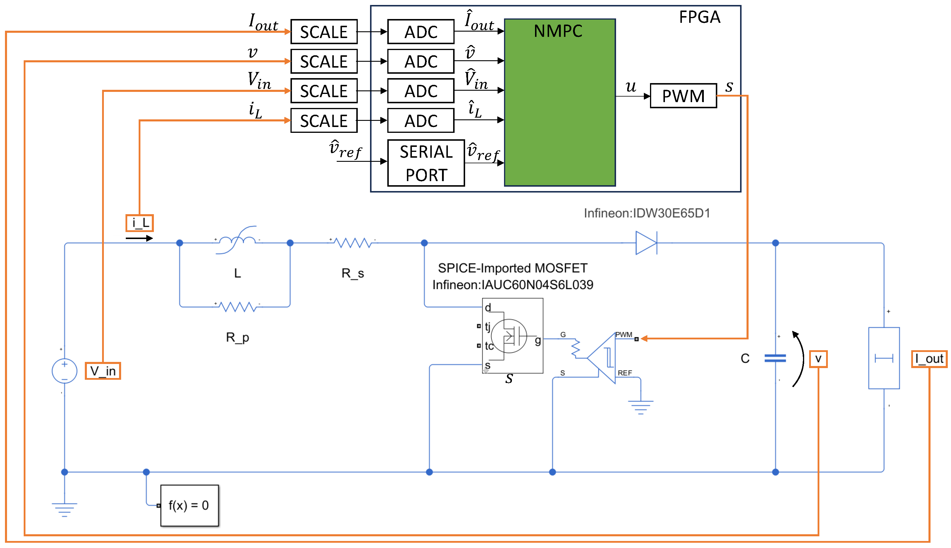
The block scheme of the complete system is shown in Figure 6. Measurements of , and collected on the boost converter are scaled to the voltage range of the analog-to-digital (ADC) converters through, e.g., an analog printed circuit board. The scaling should be such that the maximum voltages and current map into the maximum ADC voltage value. This way, the digital output of the ADC converters can be interpreted as a fixed-point number with all bits dedicated to the decimal part, leading to the normalized values , and . These signals enter the NMPC block running the MADS algorithm. The reference voltage can be provided as a digital input through, e.g., a serial port. The resulting optimal duty cycle value u is provided to a PWM generator and brought to the gate of the MOS transistor (through a proper driver).
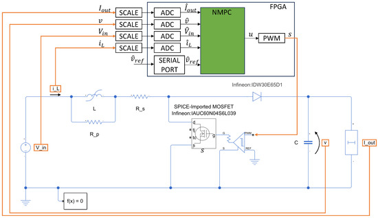
Figure 6.
Block scheme of the considered setup.
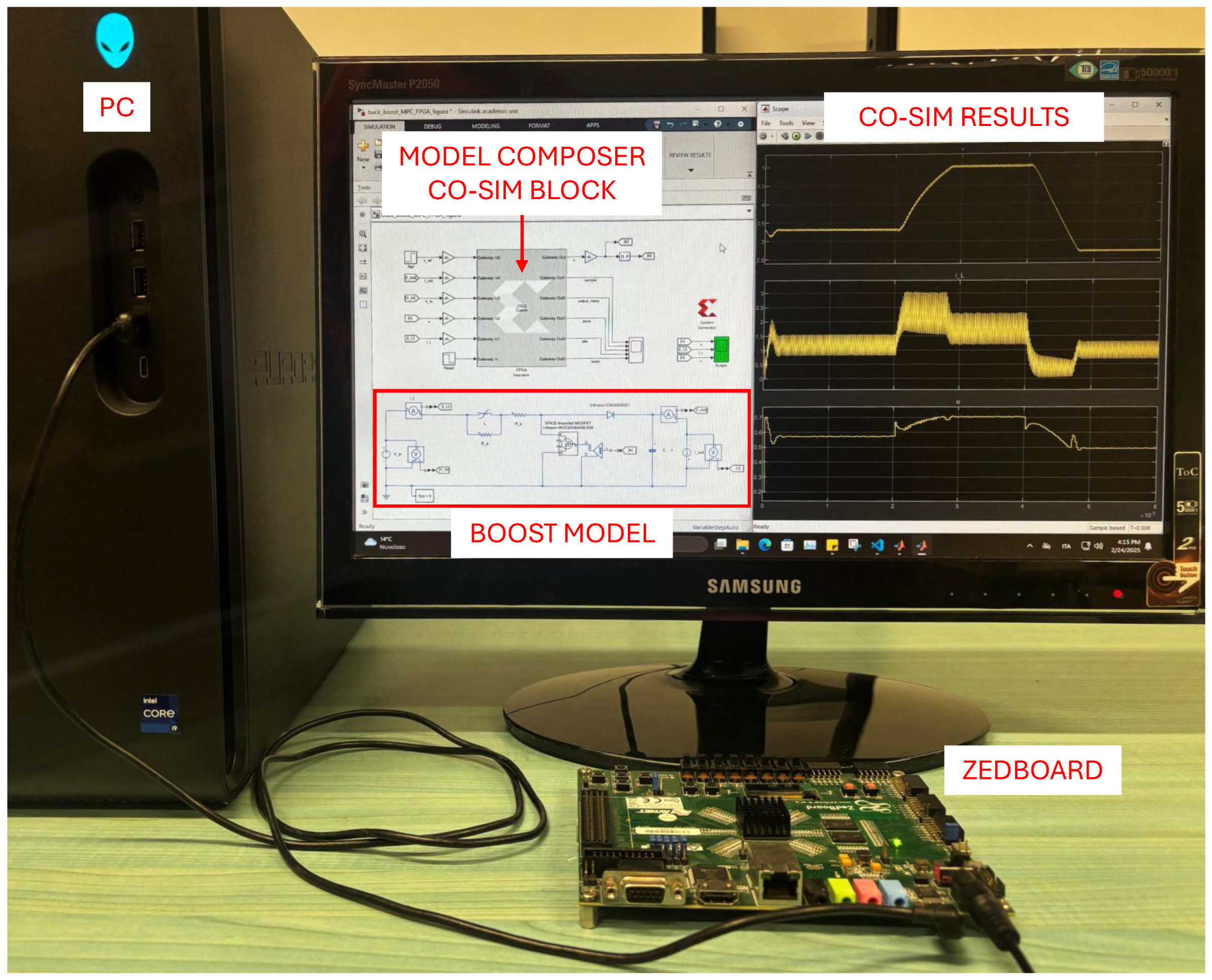
In our implementation, only the NMPC block (green) is implemented in the Zynq FPGA. All the other components in Figure 6 are simulated through Simulink R2023b. AMD Vitis Model Composer [36] is exploited to perform this hardware–software co-simulation. Figure 7 shows the adopted setup, with the Zedboard connected to a PC running Model Composer, through a USB cable.

Figure 7.
Picture of the hardware–software co-simulation.
The boost converter is modeled using the Simscape Electrical library (see Figure 6). The models of semiconductor devices are based on real components: the Infineon MOSFET IAUC60N04S6L039 [37] and the Infineon diode IDW30E65D1 [38]. A model of the gate driver for the transistor is also included. The MOSFET is modeled using the SPICE netlist provided by the manufacturer, whereas the diode is modeled based on the forward current-voltage curve provided in the datasheet. These models are more accurate than the ones used for MPC prediction, only accounting for conduction resistances and (see Figure 1).
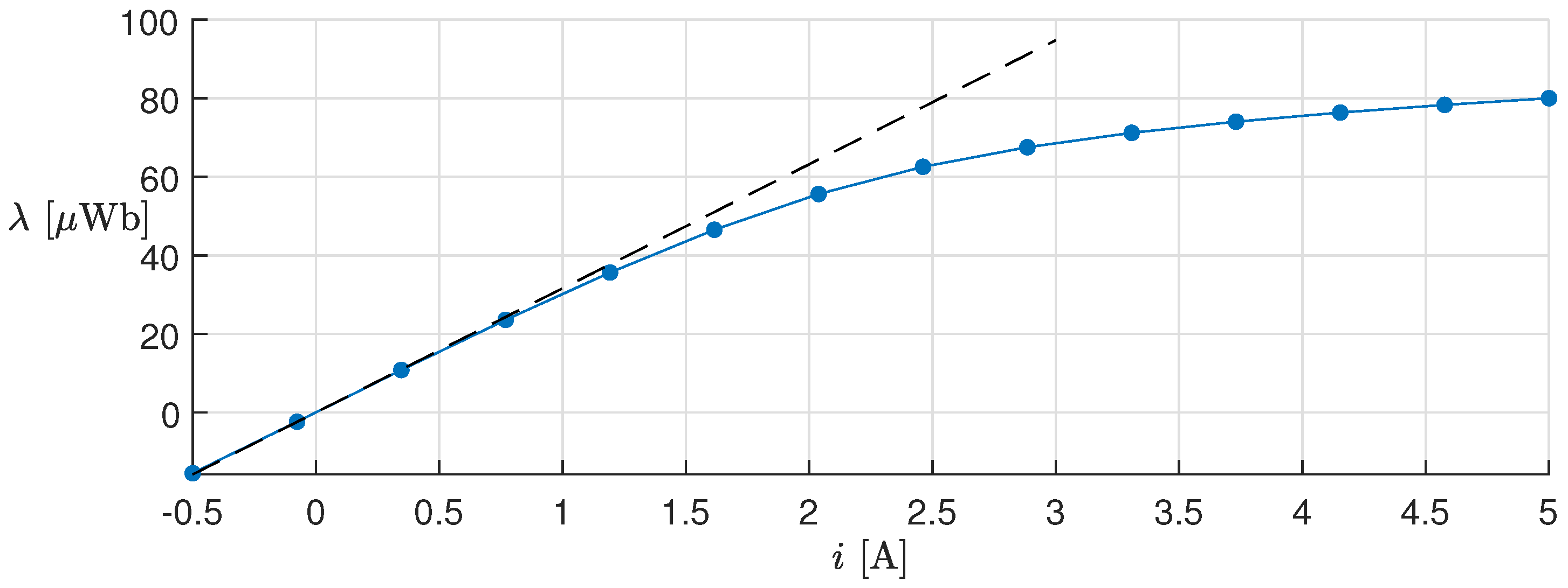
All considered parameters are listed in Table 1, whereas the piecewise-linear function is shown in Figure 8, blue curve. The black dashed curve represents the characteristics of a linear inductor. Notice that, as i approaches the maximum value ( 3 ), the inductor works in partial saturation and its characteristic drifts apart from the ideal one.

Table 1.
System parameters.
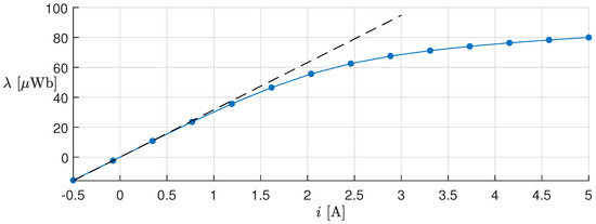
Figure 8.
Flux linkage vs. current i (blue curve). The dots mark the knee points of the curve. The black dashed line is the ideal (linear) flux linkage–current characteristic.
The values of P, Q, and R, as well as the control horizon and prediction horizon N, are selected through a heuristic process of trial and error, as there is no standard method for determining these values [39]. We remark that P, Q, and R have been chosen as powers of 2 for an efficient hardware implementation. The choice of and is discussed later in this section.
The digital circuit performance in terms of latency, used digital signal processors (DSPs), flip flops (FFs), and look-up-tables (LUTs) are listed in Table 2, both after the RTL synthesis and the place and route.
Table 2.
Circuit performance.
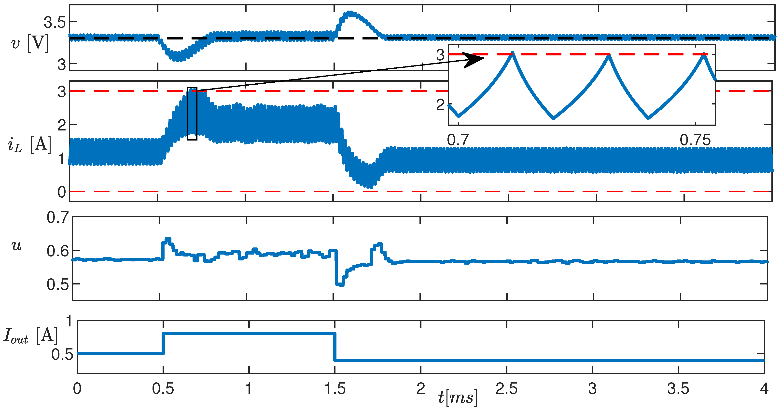
We tested the controller in three different scenarios. In the first test, is brought from 0 to in 1 (converter startup). Then, it is increased to and decreased again to . The HIL simulation results are shown in Figure 9. The four panels, from top to bottom, show v, , u, and , respectively. Notice that v correctly tracks its reference value (black dashed line) and the transients due to the change in last about (see inset). The current and the duty cycle never exceeds the constraints (red dashed lines).
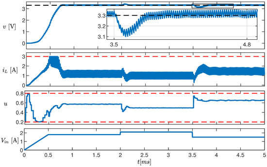
Figure 9.
Time evolution of v, , and u (top three panels) in response to a variation in (bottom panel). The red dashed lines are the imposed constraints.
In the second test (Figure 10), is changed from to , and than back to . In response to these changes, voltage v exhibits a transient (the first one lasts about ), after which it returns to its reference value. The inductor current hits both the maximum and minimum values, without exceeding them. The constraint prevents the converter from operating in discontinuous conduction mode. The inset shows a cusp-like current waveform, indicating the operation in partial magnetic saturation.
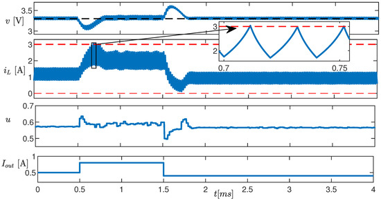
Figure 10.
Time evolution of v, , and u (top three panels) in response to a variation in (bottom panel). The red dashed lines are the imposed constraints.
In the last test (black dashed line in the top panel of Figure 11) is changed from to 5 and then back to . The output voltage is regulated to its reference value in less than 1 . The transient time depends on the fact that the current hits the imposed constraints, in both transitions.
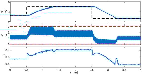
Figure 11.
Time evolution of v, , and u in response to a variation in (black dashed line). The red dashed lines are the imposed constraints.
3.2. Comparisons
The NMPC technique used in this paper was already compared to standard proportional–integral controllers in [21], as well as to MPC where the inductor is modeled as a linear component. Here we compare the performance of the controller proposed in [21], with the one implemented in this paper. We remark that this comparison is not between FPGA implementations. Instead, it shows how the changes made specifically for the FPGA implementation—the MADS optimization algorithm, the application of the control action at the next step (see Figure 4), the simplified numerical integration, and the fixed point representation—affect the control performance. The main differences are listed in Table 3.
Table 3.
Main differences between this paper and [21].
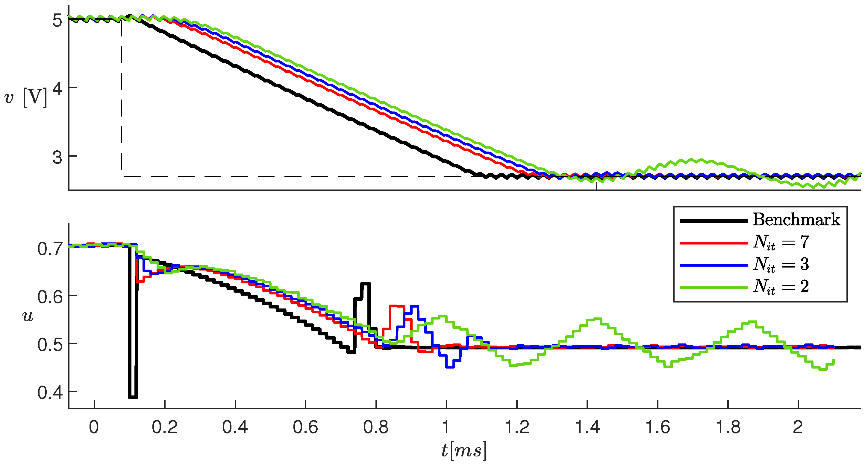
Figure 12 shows the simulation results in response to a change in obtained in [21] as a benchmark, and the new results obtained with the hardware–software co-simulation, with a different number of iterations of the MADS algorithm (see legend). The delay with respect to the benchmark case is mainly due to the fact that the control obtained based on measurements at time is applied at time . Therefore, the control response to a change in is delayed with respect to sampling time. If decreases, a suboptimal control is applied, resulting in a larger delay. With , the stationary steady state is not reached, whereas for there is no significant improvement. With , the delay in v to reach the setpoint is about 100 .
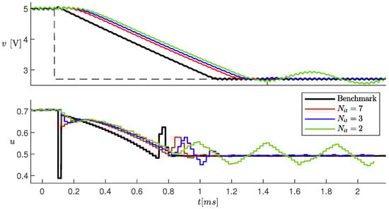
Figure 12.
Simulation results with different values of . The black curves are related to the benchmark case.
Increasing , on the other hand, impacts the circuit latency, as detailed in the next section.
3.3. Circuit Performance
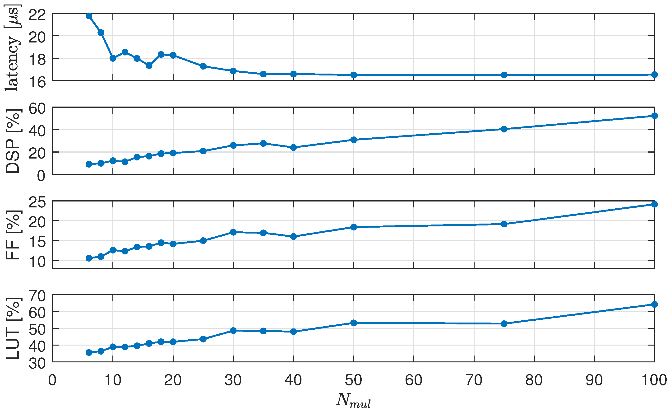
In this section, we show the digital circuit performance in response to changes in some parameters. Figure 13 shows, from top to bottom, the latency of the control algorithm, the percentage of used DSPs, FFs, and LUTs versus value applied to the #pragma directive (see Section 2.4). The latency decreases and the resource occupation increases with , as expected. However, for , the resources continue to grow, but the latency remains constant to about . For this reason, we chose in our implementation.
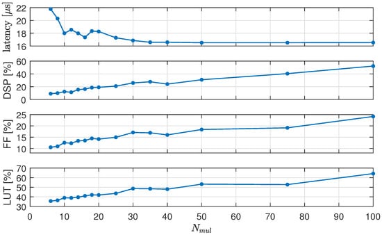
Figure 13.
From top to bottom: latency of the control algorithm, percentage of used DSPs, FFs, and LUTs vs. .
With , the RTL synthesis was performed for several combinations of N, , and . For each of them, the latency and the FPGA resource occupation are listed in Table 4. The bold line refers to the parameters used in Section 3.1. Latency increases linearly with , while resource occupation remains roughly constant. By increasing N and , the latency also increases, and the resource occupation tends to grow as well, especially LUT usage, which reaches 100% in the Zynq FPGA for . This is due to the number of evaluations of the F function, which is directly proportional to , N, and (see Equation (9)). We remark that not all parameters’ combinations listed in the table lead to good control performances, as shown in the next section. A unified design of both the control algorithm and the digital circuit is then necessary to meet all specifications.
Table 4.
Latency and FPGA resource utilization for different values of N, , and . The bold line refers to the parameters used in Section 3.1.
The effect on control when varying has already been discussed in Section 3.2. Here, the controller is tested by varying N and . Figure 14 shows some simulation results when , , and changes as shown in Section 3.1, for both and . When , the prediction horizon is too short, and the controller is ineffective; i.e., v does not reach . If N is sufficiently large—in particular, for —the controller is effective. It has been verified that increasing N beyond 5 does not further improve controller performance. Similarly, increasing from 2 to 3 does not impact control performance.
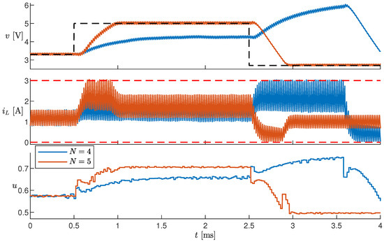
Figure 14.
Simulation results with different prediction horizons N.
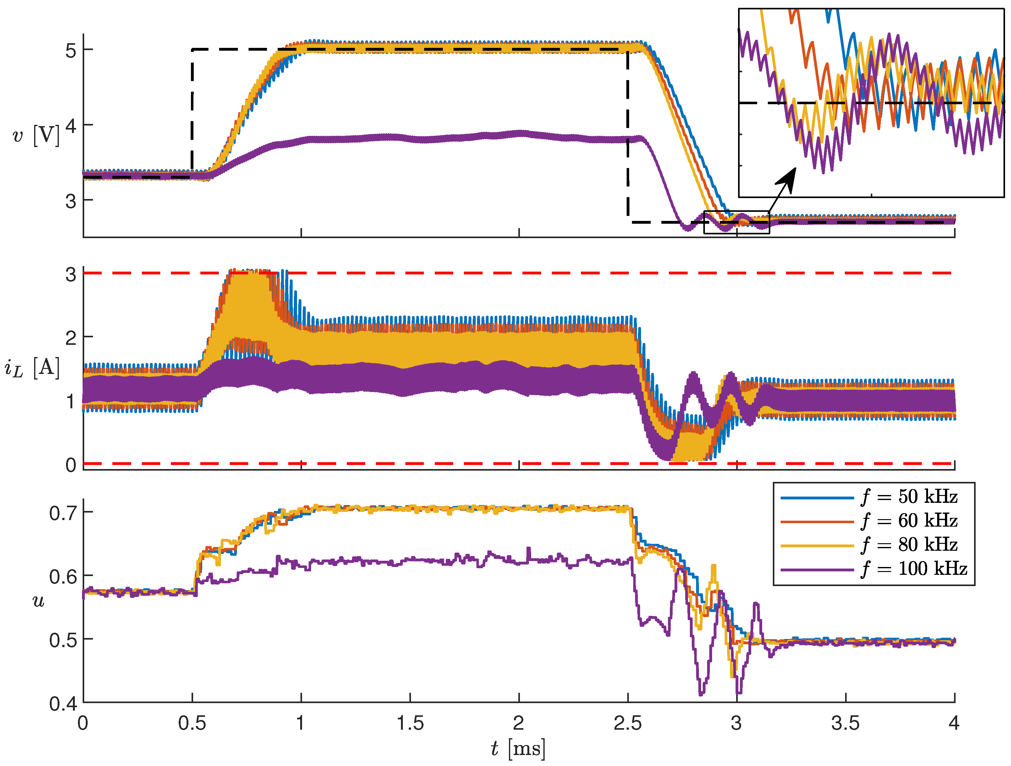
Some latencies in Table 4 are sufficiently low to allow an increase in the converter switching frequency f over 50 . For example, let us consider the case with , , and , corresponding to a latency of . In Figure 15, the scenario where changes is shown for converters operating at switching frequencies of 50 , 60 , 80 , and 100 . Up to 80 , the controller behavior is almost unchanged, with only a slight difference in the settling time of the converter output voltage (see the inset). At 100 , the controller is ineffective. In all simulations, the prediction horizon is , whereas the sampling time changes with the frequency. With 50 , the controller makes a prediction for the next 140 ; with 100 , this interval becomes shorter ( 70 ). Although the algorithm latency would allow operation up to 100 , the prediction horizon N is not long enough to ensure acceptable control performance.
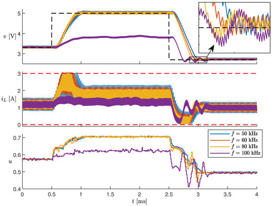
Figure 15.
Simulation results with different switching frequencies f.
4. Discussion
Traditionally, in power converters, inductor saturation is avoided by assuming a constant inductance, enabling straightforward predictions of power losses and current ripple. Under these conditions, both PI (model-free) regulators and model-based controllers, such as MPC, are effective for converter control. When the model is sufficiently accurate, MPC typically outperforms PI controllers by inherently enforcing state and input constraints.
To enhance power density in power converters, smaller inductors and higher switching frequencies can be employed to reduce current ripple and prevent saturation. In such cases, MPC requires an accurate inductor model to predict behavior near saturation. The technique proposed in [21] demonstrates that the nonlinear behavioral inductor model [9] can be effectively integrated into NMPC for voltage regulation in switching converters, even when inductors operate in partial saturation, by enforcing constraints and outperforming standard PI regulators. Conversely, using a conventional inductor model with constant inductance leads to constraint violations. This work makes a step forward with respect to [21], by implementing the NMPC controller on an FPGA and testing it through hardware–software co-simulations. This allows including the effect of data quantization, fixed-point representation, and latency, as well as the possibility to exploit simpler integration methods (e.g., the explicit midpoint) and derivative-free optimization algorithms (e.g., MADS).
This paper provides a proof of concept about the possibility of applying NMPC up to PWM frequencies of about 80 . It should be noted that the presented results are valid for the specific converter used in this work. When employing a different converter, its dynamics may vary, so the maximum achievable switching frequency may vary. Therefore, the selection of the parameters N, , and must be evaluated case by case.
The next step will be to apply the embedded controller to a real boost converter.
5. Conclusions
In this work, an NMPC technique for the control of a boost converter with a nonlinear inductor is implemented on an FPGA. The hardware–software co-simulation results show that the embedded controller is able to regulate the converter’s output voltage by fulfilling current constraints, even when the inductor operates at partial magnetic saturation, up to PWM frequencies of about 80 . Further work will be concerned with the real-time control of a real boost converter, thus assessing its robustness against measurement noise and model inaccuracies.
Author Contributions
Conceptualization, A.O.; Methodology, M.L.; Software, A.R. and A.O.; Validation, A.R.; Data curation, M.L.; Writing—original draft, A.O.; Writing—review & editing, M.S.; Supervision, M.S. All authors have read and agreed to the published version of the manuscript.
Funding
This work was partially funded by the European Union-NextGenerationEU, within the project “MAGSAT-Exploiting MAGnetic SATuration to increase power density in switching converters”, University of Genoa, Italy.
Data Availability Statement
Data are contained within the article.
Conflicts of Interest
The authors declare no conflicts of interest.
Appendix A
We start from Equations (5) and (6) in [21], where the state variables are v and i. Here, we perform a change of variables by considering that and . Therefore, we obtain the differential equations for state :
The current can be expressed as
Appendix B
For the FPGA implementation, it is important to spare time and resources. Therefore, we define the following (dimensionless) constants that can be computed offline and stored in the circuit memory.
The parameters depend on T; therefore, they must be updated if the converter’s switching frequency is changed.
Recall that, in the MPC prediction phase, the values of and are assumed to be constant. By referring to Equation (3), the integration is performed through the following operations.
References
- Milner, L.; Rincón-Mora, G.A. Small saturating inductors for more compact switching power supplies. IEEJ Trans. Electr. Electron. Eng. 2012, 7, 69–73. [Google Scholar] [CrossRef]
- Di Capua, G.; Femia, N. A novel method to predict the real operation of ferrite inductors with moderate saturation in switching power supply applications. IEEE Trans. Power Electron. 2016, 31, 2456–2464. [Google Scholar] [CrossRef]
- Di Capua, G.; Femia, N.; Stoyka, K. Impact of Inductors Saturation on DC–DC Switching Regulators. In Proceedings of the IEEE International Forum on Research and Technology for Society and Industry (RTSI), Florence, Italy, 9–12 September 2019; pp. 254–259. [Google Scholar]
- Scirè, D.; Lullo, G.; Vitale, G. Assessment of the Current for a Non-Linear Power Inductor Including Temperature in DC–DC Converters. Electronics 2023, 12, 579. [Google Scholar] [CrossRef]
- Oliveri, A.; Lodi, M.; Storace, M. Nonlinear models of power inductors: A survey. Int. J. Circuit Theory Appl. 2022, 1, 2–34. [Google Scholar] [CrossRef]
- Scirè, D.; Lullo, G.; Vitale, G. Non-Linear Inductor Models Comparison for Switched-Mode Power Supplies Applications. Electronics 2022, 11, 2472. [Google Scholar] [CrossRef]
- Kaiser, J.; Duerbaum, T. An overview of saturable inductors: Applications to power supplies. IEEE Trans. Power Electron. 2021, 36, 10766–10775. [Google Scholar] [CrossRef]
- Ravera, A.; Formentini, A.; Lodi, M.; Oliveri, A.; Passalacqua, M.; Storace, M. Modeling the Effect of Air-Gap Length and Number of Turns on Ferrite-Core Inductors Working up to Magnetic Saturation in a Buck Converter. IEEE Trans. Circ. Syst. I 2024, 71, 5400–5409. [Google Scholar] [CrossRef]
- Ravera, A.; Oliveri, A.; Lodi, M.; Storace, M. A nonlinear behavioral model of a ferrite-core inductor with fixed-frequency sinusoidal voltage input. In Proceedings of the IEEE International Conference on Smart Techonologies (EUROCON), Turin, Italy, 6–8 July 2023. [Google Scholar]
- Ravera, A.; Oliveri, A.; Lodi, M.; Beatrice, C.; Ferrara, E.; Fiorillo, F.; Storace, M. Modeling Amorphous-Core Inductors up to Magnetic Saturation. IEEE Trans. Power Electron. 2024, 40, 1563–1576. [Google Scholar] [CrossRef]
- Ravera, A.; Oliveri, A.; Lodi, M.; Bemporad, A.; Heemels, W.; Kerrigan, E.C.; Storace, M. Co-Design of a Controller and Its Digital Implementation: The MOBY-DIC2 Toolbox for Embedded Model Predictive Control. IEEE Trans. Control Syst. Technol. 2023, 31, 2871–2878. [Google Scholar] [CrossRef]
- Karamanakos, P.; Geyer, T.; Oikonomou, N.; Kieferndorf, F.D.; Manias, S. Direct model predictive control: A review of strategies that achieve long prediction intervals for power electronics. IEEE Ind. Electron. Mag. 2014, 8, 32–43. [Google Scholar] [CrossRef]
- Muthukumar, P.; Venkateshkumar, M.; Chin, C.S. A Comparative Study of Cutting-Edge Bi-Directional Power Converters and Intelligent Control Methodologies for Advanced Electric Mobility. IEEE Access 2024, 12, 28710–28752. [Google Scholar] [CrossRef]
- Liu, Y.C.; Ge, X.; Tang, Q.; Deng, Z.; Gou, B. Model predictive current control for four-switch three-phase rectifiers in balanced grids. Electron. Lett. 2017, 53, 44–46. [Google Scholar] [CrossRef]
- Jin, T.; Wei, H.; Legrand, D.; Nzongo, M.; Zhang, Y. Model predictive control strategy for NPC grid-connected inverters in unbalanced grids. Electron. Lett. 2016, 52, 1248–1250. [Google Scholar] [CrossRef]
- Wu, J.; Li, J.; Wang, H.; Li, G.; Ru, Y. Fault-Tolerant Three-Vector Model-Predictive-Control-Based Grid-Connected Control Strategy for Offshore Wind Farms. Electronics 2024, 13, 2316. [Google Scholar] [CrossRef]
- Bououden, S.; Hazil, O.; Filali, S.; Chadli, M. Modelling and model predictive control of a DC–DC Boost converter. In Proceedings of the 2014 15th International Conference on Sciences and Techniques of Automatic Control and Computer Engineering (STA), Hammamet, Tunisia, 21–23 December 2024; IEEE: Piscataway, NJ, USA, 2014; pp. 643–648. [Google Scholar]
- Lekić, A.; Hermans, B.; Jovičić, N.; Patrinos, P. Microsecond nonlinear model predictive control for DC–DC converters. Int. J. Circuit Theory Appl. 2020, 48, 406–419. [Google Scholar] [CrossRef]
- Stickan, B.; Frison, G.; Burger, B.; Diehl, M. A nonlinear Real-Time Pulse-Pattern MPC Scheme for Power-Electronics Circuits Operating in the Microseconds Range. In Proceedings of the American Control Conference, Atlanta, GA, USA, 8–10 June 2022; pp. 2070–2077. [Google Scholar]
- Mariethoz, S.; Herceg, M.; Kvasnica, M. Model Predictive Control of buck DC–DC converter with nonlinear inductor. In Proceedings of the 11th Workshop on Control and Modeling for Power Electronics, Zurich, Switzerland, 17–20 August 2008; pp. 1–8. [Google Scholar]
- Firpo, P.; Ravera, A.; Oliveri, A.; Lodi, M.; Storace, M. Use of a Partially Saturating Inductor in a Boost Converter with Model Predictive Control. Electronics 2023, 12, 3013. [Google Scholar] [CrossRef]
- McInerney, I.; Constantinides, G.A.; Kerrigan, E.C. A Survey of the Implementation of Linear Model Predictive Control on FPGAs⁎⁎The support of the EPSRC Centre for Doctoral Training in High Performance Embedded and Distributed Systems (HiPEDS, Grant Reference EP/L016796/1) is gratefully acknowledged. IFAC-PapersOnLine 2018, 51, 381–387. [Google Scholar] [CrossRef]
- Xu, F.; Guo, Z.; Chen, H.; Ji, D.; Qu, T. A Custom Parallel Hardware Architecture of Nonlinear Model Predictive Control on FPGA. IEEE Trans. Ind. Electron. 2022, 69, 11569–11579. [Google Scholar] [CrossRef]
- Guo, H.; Liu, F.; Xu, F.; Chen, H.; Cao, D.; Ji, Y. Nonlinear model predictive lateral stability control of active chassis for intelligent vehicles and its FPGA implementation. IEEE Trans. Syst. Man Cybern. Syst. 2017, 49, 2–13. [Google Scholar] [CrossRef]
- Ravera, A.; Oliveri, A.; Lodi, M.; Storace, M. MADS-based fast FPGA implementation of nonlinear model predictive control. In Proceedings of the IEEE International Symposium on Circuits and Systems, Monterey, CA, USA, 21–25 May 2023. [Google Scholar]
- Englert, T.; Völz, A.; Mesmer, F.; Rhein, S.; Graichen, K. A software framework for embedded nonlinear model predictive control using a gradient-based augmented Lagrangian approach (GRAMPC). Optim. Eng. 2019, 20, 769–809. [Google Scholar] [CrossRef]
- Hausberger, T.; Kugi, A.; Eder, A.; Kemmetmüller, W. High-speed nonlinear model predictive control of an interleaved switching DC/DC-converter. Control Eng. Pract. 2020, 103, 104576. [Google Scholar] [CrossRef]
- Patne, V.; Ingole, D.; Sonawane, D. FPGA Implementation Framework for Low Latency Nonlinear Model Predictive Control. IFAC-PapersOnLine 2020, 53, 7020–7025. [Google Scholar] [CrossRef]
- Ravera, A.; Oliveri, A.; Lodi, M.; Storace, M. Embedded Linear Model Predictive Control Through Mesh Adaptive Direct Search Algorithm. In Proceedings of the 2019 26th IEEE International Conference on Electronics, Circuits and Systems (ICECS), Genoa, Italy, 27–29 November 2019; pp. 542–545. [Google Scholar] [CrossRef]
- Khusainov, B.; Kerrigan, E.C.; Constantinides, G.A. Automatic Software and Computing Hardware Codesign for Predictive Control. IEEE Trans. Control Syst. Technol. 2019, 27, 2295–2304. [Google Scholar] [CrossRef]
- Audet, C.; Dennis, J.E., Jr. Mesh adaptive direct search algorithms for constrained optimization. SIAM J. Optim. 2006, 17, 188–217. [Google Scholar] [CrossRef]
- Audet, C.; Dennis, J.E. A Progressive Barrier for Derivative-Free Nonlinear Programming. SIAM J. Optim. 2009, 20, 445–472. [Google Scholar] [CrossRef]
- Süli, E.; Mayers, D.F. An Introduction to Numerical Analysis; Cambridge University Press: Cambridge, UK, 2003. [Google Scholar]
- AMD. Vitis Reference Guide; Technical Report UG1702 (v2024.2); AMD, Inc.: Sunnyvale, CA, USA, 2025. [Google Scholar]
- Lucia, S.; Navarro, D.; Lucia, O.; Zometa, P.; Findeisen, R. Optimized FPGA implementation of model predictive control for embedded systems using high-level synthesis tool. IEEE Trans. Ind. Inform. 2017, 14, 137–145. [Google Scholar] [CrossRef]
- AMD. Vitis Model Composer Reference Guide; Technical Report UG1483 (v2024.2); AMD, Inc.: Sunnyvale, CA, USA, 2025. [Google Scholar]
- Infineon. OptiMOS™-6 Power-Transistor—IAUC60N04S6L039. 2019. Available online: https://www.infineon.com/dgdl/Infineon-IAUC60N04S6L039-DataSheet-v01_00-EN.pdf?fileId=5546d4626afcd350016b1c511cb70df6 (accessed on 24 February 2025).
- Infineon. IDW30E65D1—Emitter Controlled Diode Rapid 1 Series. 2013. Available online: https://www.infineon.com/dgdl/Infineon-IDW30E65D1-DS-v02_02-en.pdf?fileId=db3a30433d68e984013d6929d1da01cc (accessed on 24 February 2025).
- Grüne, L.; Pannek, J. Nonlinear Model Predictive Control; Springer: Berlin/Heidelberg, Germany, 2017. [Google Scholar]


Disclaimer/Publisher’s Note: The statements, opinions and data contained in all publications are solely those of the individual author(s) and contributor(s) and not of MDPI and/or the editor(s). MDPI and/or the editor(s) disclaim responsibility for any injury to people or property resulting from any ideas, methods, instructions or products referred to in the content. |
© 2025 by the authors. Licensee MDPI, Basel, Switzerland. This article is an open access article distributed under the terms and conditions of the Creative Commons Attribution (CC BY) license (https://creativecommons.org/licenses/by/4.0/).