Article

Research on the Nonlinear Dynamic Characteristics of Fractional-Order Flyback Converter Based on Generalized Euler Method

School of Electrical Engineering, Guangxi University, Nanning 530004, China
*
Author to whom correspondence should be addressed.
Electronics 2025, 14(5), 977; https://doi.org/10.3390/electronics14050977
Submission received: 11 January 2025 / Revised: 20 February 2025 / Accepted: 25 February 2025 / Published: 28 February 2025

Abstract

:
The nonlinear dynamic characteristics of a peak current regulation fractional-order (FO) flyback converter, considering the fractional nature of inductance and capacitance, are investigated in detail. First, the discrete iterative model of the fractional-order (FO) flyback converter under 10 kHz operating conditions is accomplished using the application of the Generalized Euler Method (GEM). On this basis, bifurcation diagrams, phase diagrams, and simulated time domain diagrams are used to describe the nonlinear dynamic behavior of the converter. The nonlinear dynamics of the converter are investigated through bifurcation and phase diagram analyses. A comprehensive examination is conducted to evaluate the impact of key parameters, including input voltage, reference current, and the fractional orders of inductance and capacitance, on the system’s stability. Furthermore, a comparative analysis is performed with conventional integer-order (IO) flyback converters to highlight the distinctive characteristics. The findings demonstrate that the FO converter manifests distinct nonlinear characteristics, including period-doubling bifurcation and chaotic behavior. Moreover, for identical parameter sets, the FO flyback converter is found to possess a smaller stability domain but a larger parameter region for bifurcation and chaos compared to its IO counterpart. This behavior allows the FO converter to more accurately capture the nonlinear dynamic characteristics of the flyback converter. Simulation results further substantiate the theoretical predictions.

1. Introduction

A flyback converter has the characteristics of high reliability, strong controllability, strong adaptability, small size and low cost. It is widely used in the fields of electric vehicle charging [1], solar photovoltaic systems [2], and motor drives [3].
As a result, there is a growing demand for enhanced stability and reliability in these converters. Flyback converters constitute a category of inherently nonlinear time-varying systems, demonstrating complex dynamic behaviors and rich nonlinear characteristics. Chaos, as a typical nonlinear phenomenon, can significantly affect the stability of flyback converters, leading to undesirable voltage and current oscillations. Such instability poses substantial challenges to system performance, particularly in applications requiring high stability and precision. Therefore, a comprehensive investigation of the nonlinear dynamics is essential for gaining profound insights into the operational behavior of flyback converters. This is beneficial for optimizing circuit parameters, improving system stability and power quality, and reducing electromagnetic interference. The literature [4] established a sampled-data model for the flyback converter controlled by Peak Current Mode (PCM) and derived the critical stability equations using the Jacobian matrix, but it did not delve into the nonlinear dynamic behavior of the converter. The literature [5] proposed a direct output voltage control method based on feedback linearization, but it employed integer-order modeling, which fails to accurately describe the non-integer dynamic behavior of the system under high-frequency electromagnetic conditions. In contrast, fractional-order modeling can more precisely characterize the dynamic properties of inductors and capacitors, revealing the complex nonlinear behaviors of the flyback converter under high-frequency conditions, such as period-doubling bifurcations and low-frequency oscillations. This modeling approach not only provides a theoretical foundation for chaos control to ensure stable system operation but also offers more comprehensive theoretical support for the design of flyback converters [6,7]. Based on the fact that real inductors and capacitors exhibit fractional-order characteristics, researchers have initiated studies on fractional-order converters. The FO model is used to analyze the converter, which is more consistent with essence than the IO model [8]. In the literature [9], a FO piecewise smoothing model of the converter, including the resonant capacitance impedance model, is presented, and it provides a better explanation of the microscopic phenomena of the resonant converter. Additionally, ref. [10] demonstrates that the fractional order of inductance and capacitance significantly influences steady-state parameters, including output voltage and current ripple amplitude, especially in discontinuous conduction mode converters. In ref. [11], by combining the main oscillation solution derived from the simplified equivalent circuit model with the steady state solution based on equivalent small parameter method, the accurate analytical solution derived from the mathematical model of FO very high frequency converter is effectively analyzed. Ref. [12] employs a predictive correction algorithm to demonstrate that fractional-order buck-boost converters exhibit bifurcation phenomena and chaotic nonlinearities under specific operational conditions and parameter configurations. Furthermore, the study reveals distinct stability parameter domains between fractional-order buck-boost converters and their integer-order counterparts. In ref. [13], the low-frequency oscillations in flyback converters are investigated through the application of a fractional-order small-signal model, enabling precise prediction of the system’s operational stability region.
At present, most FO converter research has focused on the basic converter, such as buck [14] and buck-boost [15] converters, and there has been less research examining flyback converters. Most studies of the flyback converter are based on the IO converters, which is inconsistent with the FO nature of converters. The response characteristics of the FO converter can be studied by solving the FO state space average model. The FO state space average model is a FO differential equation with state variables based on Kirchhoff’s law and component characteristics. Numerical solutions to fractional differential equations include the generalized Euler method [16], predictive correction method [17], finite element method [18], Runge–Kutta method [19], difference method [20], et al. Compared with other methods, the generalized Euler method has the advantages of simple solutions, small computations, and good stability, and has been widely used in epidemiology, environmental science, and other fields [21,22]. For these reasons, this study investigates the period-doubling bifurcation and chaotic behavior in FO flyback converters through the application of nonlinear dynamical system theory and fractional calculus principles. It aims to reveal the complex dynamic behaviors of FO flyback converters, provide theoretical support for high-frequency power supply design, and address the challenges of high computational load and poor stability in the simulation of FO flyback converters.
The paper is organized as follows. First, the GEM is briefly introduced in Section 2; then, in Section 3, the discrete mathematical model of the FO flyback converter is constructed using the (GEM). Section 4 presents a comprehensive nonlinear dynamics analysis, through which the bifurcation diagrams, V–I phase portraits, and simulated time domain diagrams are systematically derived. Finally, the conclusion is drawn in Section 5.

2. Materials and Methods

GEM is proposed by Odibat et al. [16]. This method represents an advanced extension of the classical Euler approach, demonstrating superior numerical stability and enhanced computational precision in FO system applications.
The Caputo fraction definition is as follows:
D * q y ( x ) = f ( x , y ( x ) ) , y ( 0 ) = y 0
where q is the fractional differential operator, 0 < q 1 , the independent variable x > 0 , and y 0 is the initial value.
According to the literature [23], the generalized Taylor formula for function y ( x ) with a known value y ( a ) is as follows:
y ( x ) = y ( a ) + n = 1 y q n ( a ) Γ ( q n + 1 ) ( x a ) q n
where y q n ( a ) represents the q n derivative of function y ( x ) at point a , 0 < q n < 1 . Γ is a gamma function.
According to the GEM, let t j = j h , where j = 0 , 1 , , k and k is an integer. Divide an interval into equal parts. The interval 0 , p is divided into k subintervals t j , t j + 1 with width h = p k . Let y ( t ) , D * q y ( t ) , and D * 2 q y ( t ) be continuously differentiable at [ 0 , p ] , the expression of y ( t ) with respect to t = t 0 by using (2) to expand is as:
y ( t ) = y ( t 0 ) + ( D * q y ( t ) ) ( t 0 ) t q Γ ( q + 1 ) + ( D * 2 q y ( t ) ) ( c 1 ) t 2 q Γ ( 2 q + 1 )
Substituting ( D * q y ( t ) ) ( t 0 ) = f ( t 0 , y ( t 0 ) ) and h = t 1 into (3), y ( t 1 ) can be expressed as follows:
y ( t 1 ) = y ( t 0 ) + f ( t 0 , y ( t 0 ) ) h q Γ ( q + 1 ) + ( D * 2 q y ( t ) ) ( c 1 ) h 2 q Γ ( 2 q + 1 )
Assuming h is small, and omitting the higher order terms, we obtain:
y ( t 1 ) = y ( t 0 ) + h q Γ ( q + 1 ) f ( t 0 , y ( t 0 ) )
y ( t j + 1 ) = y ( t j ) + h q Γ ( q + 1 ) f ( t j , y ( t j ) )

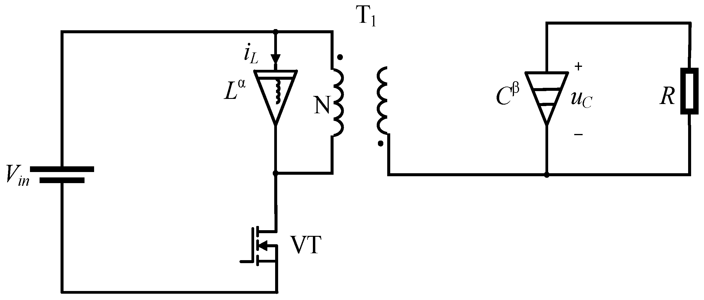
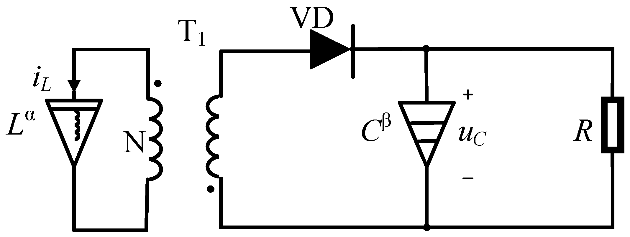
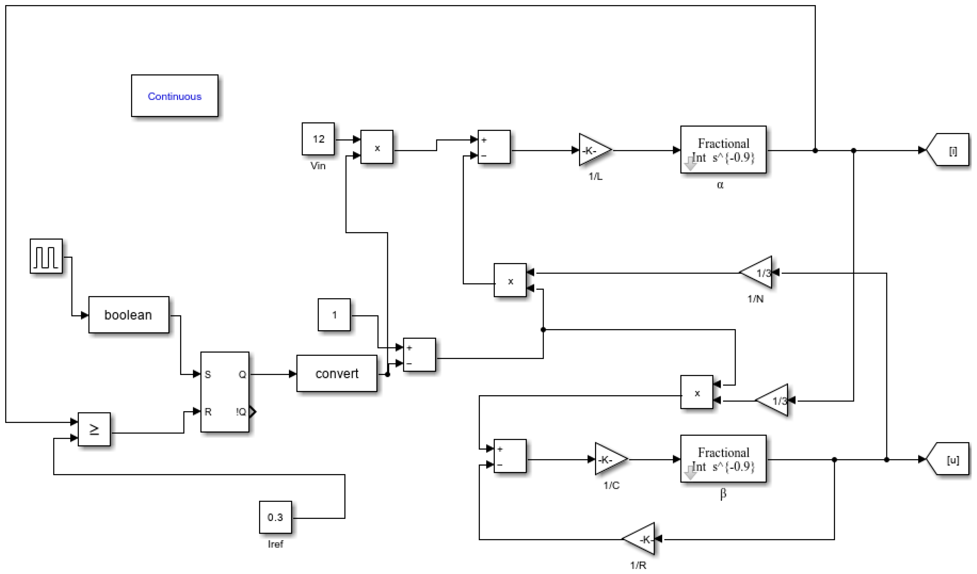
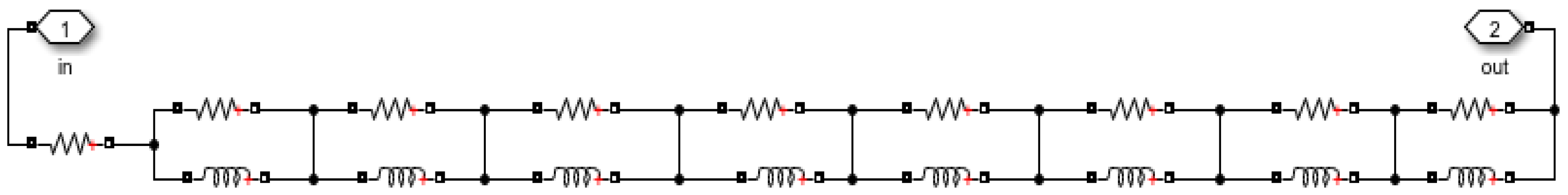
3. Mathematical Model of FO Flyback Converter

The schematic diagram of the FO flyback converter incorporating peak current-mode control is illustrated in Figure 1, in which Vin is the input voltage, the inductor Lα is the FO inductor with the FO α, the capacitor Cβ is the FO capacitor with the FO β, R is the load, T1 is an ideal transformer with a ratio of N:1, and the switch VT and VD are ideal.
The relationship between the inductor voltage uL and capacitor current ic of the FO components are given by [24]
u L α = L d α i L d t α i c β = C d β u C d t β
when converter operates in continuous current mode (CCM), two operating modes can be identified as:
Mode 1 n T < t < ( n + d ) T : VT is on, VD is off. The circuit topology corresponding to the specific operating mode is illustrated in Figure 2. The state equations are:
d α i L d t α = 1 L V i n d β u C d t β = 1 R C β u C
Mode 2 ( n + d ) T < t < ( n + 1 ) T : VT is off, VD is on. The schematic diagram of the circuit topology for the specific operating mode is presented in Figure 3. The state equations are:
d α i L d t α = 1 N L u C d β u C d t β = 1 N C i L 1 R C u C
The nonlinear switching function S t is defined as a binary control variable, where S t = 1 indicates the ON state of switch S, while S t = 0 corresponds to its OFF state. The mathematical representation of S(t) can be expressed as follows:
S ( t ) = 1 , n T < t < ( n + d ) T 0 , ( n + d ) T < t < ( n + 1 ) T
According to the state space averaging method, the FO state space model of FO flyback converter in CCM can be obtained from (8)–(10) as follows:
d α i L d t α = S 1 L V i n ( 1 S ) 1 N L u C d β u C d t β = ( 1 S ) 1 N C i L 1 R C u C
The discrete model of FO CCM flyback converter is by using:
i n + 1 = i n + h α Γ ( α + 1 ) ( S 1 L V i n ( 1 S ) 1 N L u n ) u n + 1 = u n + h β Γ ( β + 1 ) ( ( 1 S ) 1 N C i n 1 R C u n )
where h = T N 0 , {tn = nh, n = 0, 1, …, N0}, (N0 is the number of points calculated in each cycle T). When α = β = 1 , Equation (12) is the discrete mathematical model of the IO flyback converter. Based on Equation (12), the Simulink mathematical model can be constructed as shown in Figure 4.

4. Nonlinear Dynamics Analysis

The circuit parameters of the FO flyback converter are provided in Table 1. The simulation model of the FO flyback converter is developed using Matlab R2023 b/Simulink, as illustrated in Figure 5. Figure 6 and Figure 7 respectively present the equivalent circuit topologies incorporating FO capacitors and inductors with a fractional order of 0.9. The equivalent capacitance and inductance values for the 0.9-order system are presented in Table 2.

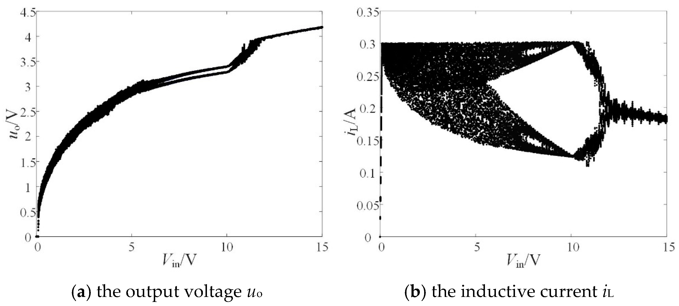
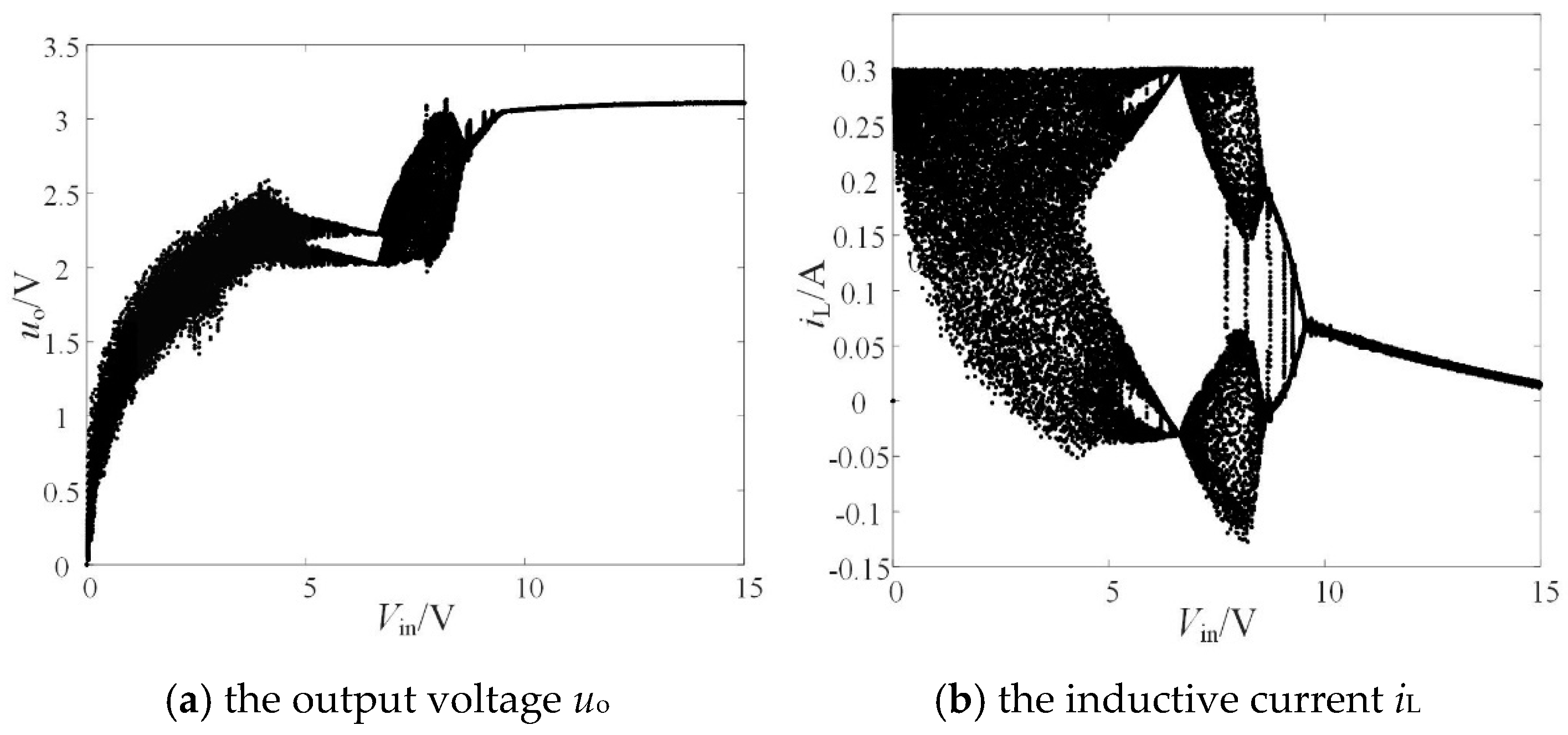
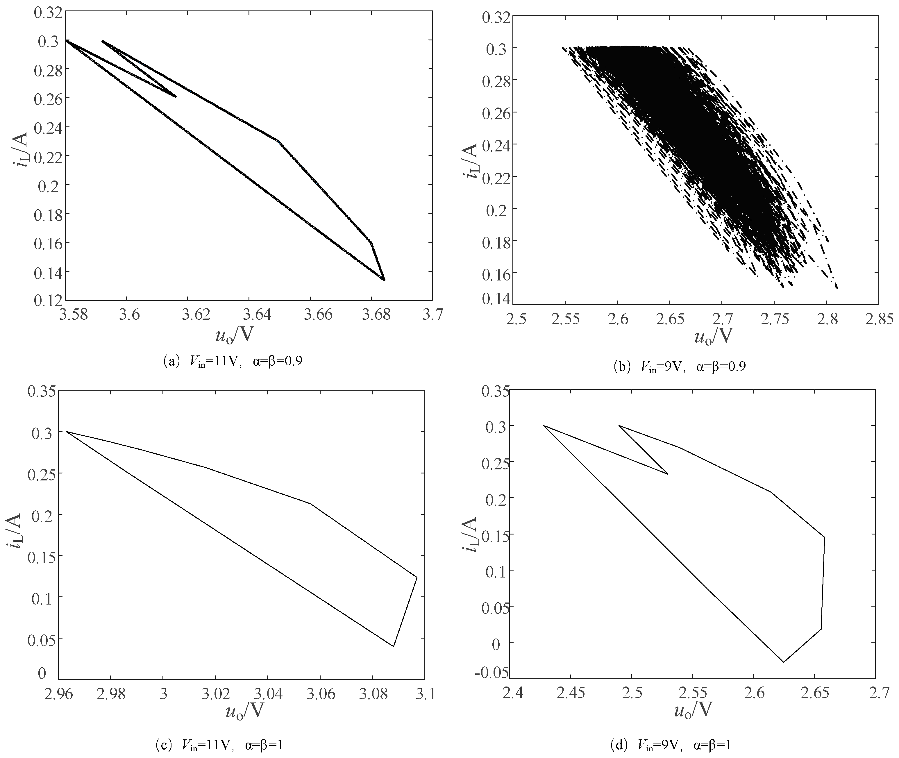
4.1. Input Voltage Vin as the Bifurcation Parameter

The bifurcation diagram is an important tool for studying the nonlinear behavior of dynamical systems, which can reveal the stability, periodicity, and chaos of the system as parameters change. In other words, it examines the impact of perturbing a single parameter on the global dynamical behavior of the output variable. The derived mathematical model (12) can be used in Matlab R2023b to predict the output values of the Flyback converter under different parameter conditions. The bifurcation diagrams, with input voltage Vin as the bifurcation parameter and keeping the other circuit parameters as shown in Table 1, are presented in Figure 8 and Figure 9 for both the FO and IO converters, respectively.
As Figure 8 shows, when Vin > 11.9 V, the FO flyback converter is in stable operation. When Vin = 11.9 V, the system has a period-doubling bifurcation for the first time and enters the period 2 running state. When Vin < 10.16 V, the system goes to chaos.
As shown in Figure 9, when Vin > 9.76 V, the IO flyback converter maintains a stable operating state. When Vin = 9.76 V, the system appears the first period-doubling bifurcation and enters the period 2 operation state. When Vin < 8.65 V, the system goes to chaos.
From Figure 8 and Figure 9, the comparative analysis of operational characteristics between FO and IO flyback converters across varying input voltage conditions is systematically presented in Table 3. The experimental data reveal that, under identical parametric conditions, the FO converter demonstrates a significantly narrower stable operating region compared to its IO counterpart. The FO converter has a period doubling bifurcation when Vin = 11.9 V, but the IO converter is still in a stable operating state.

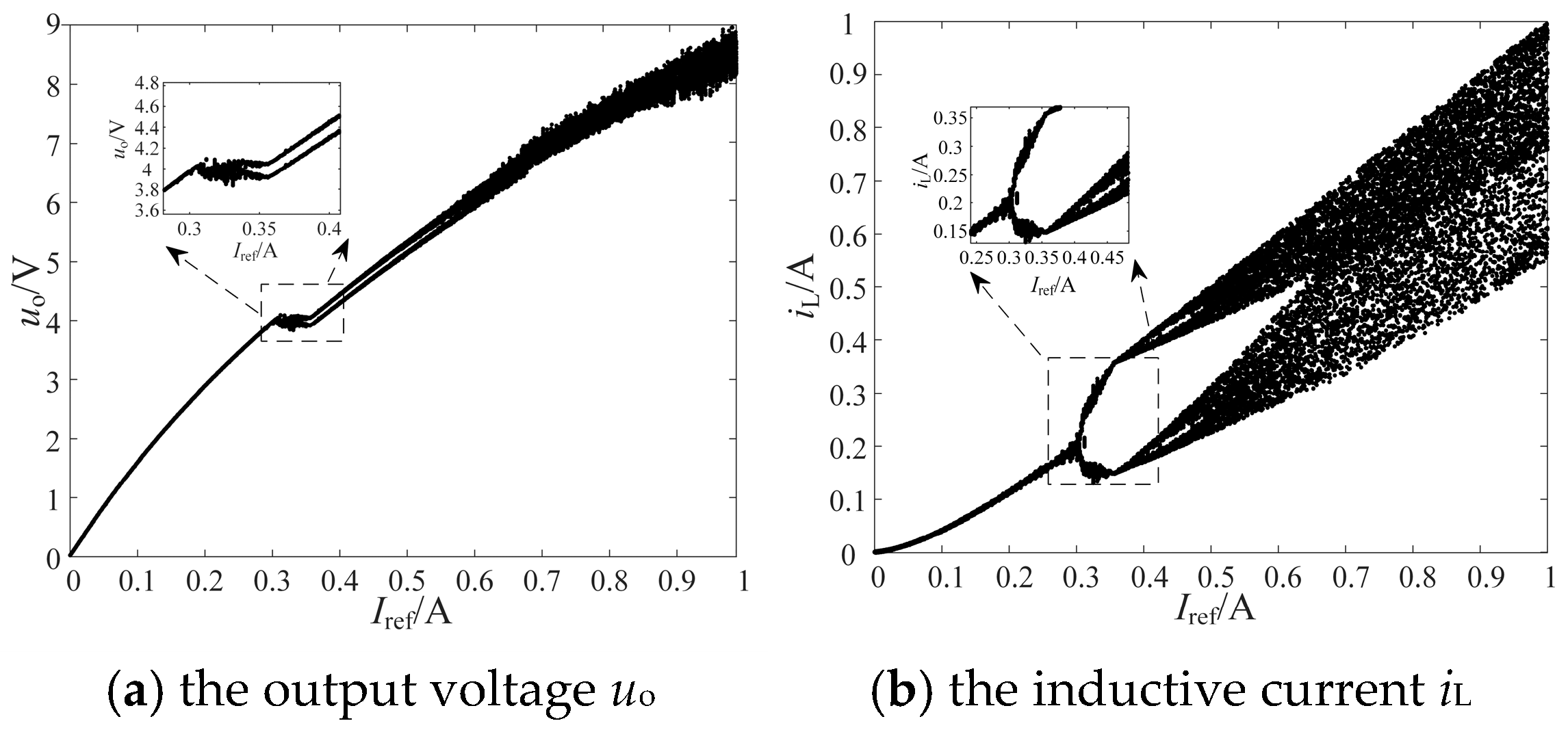
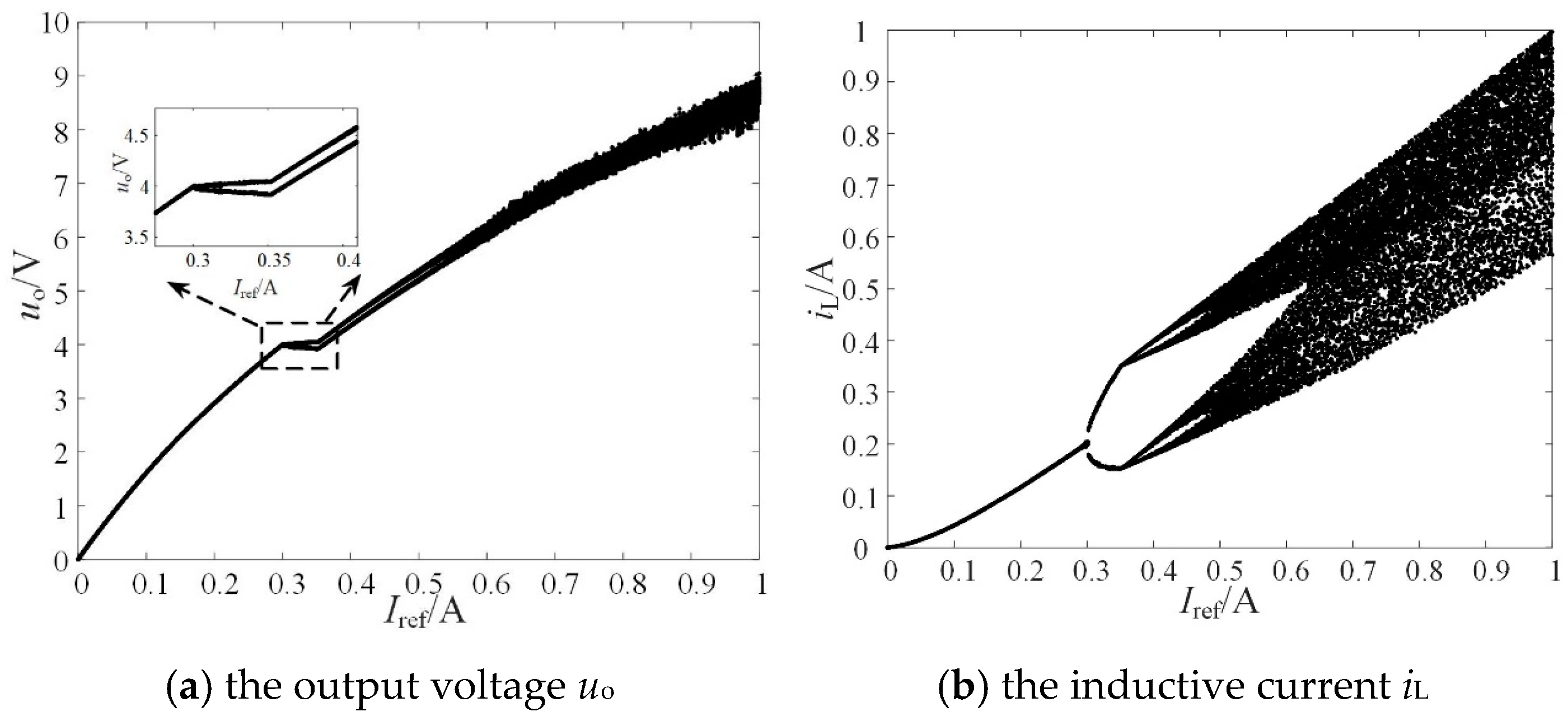
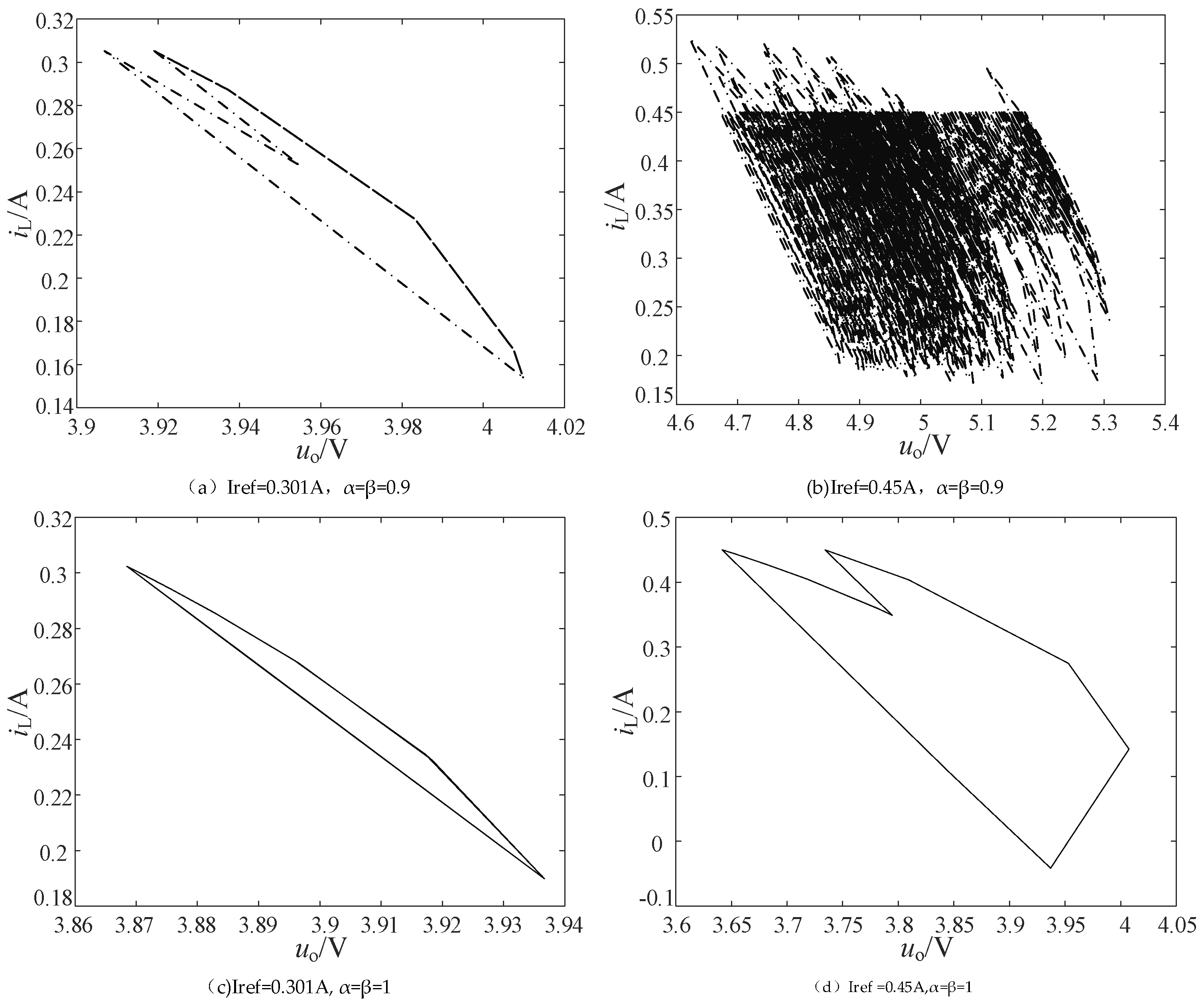
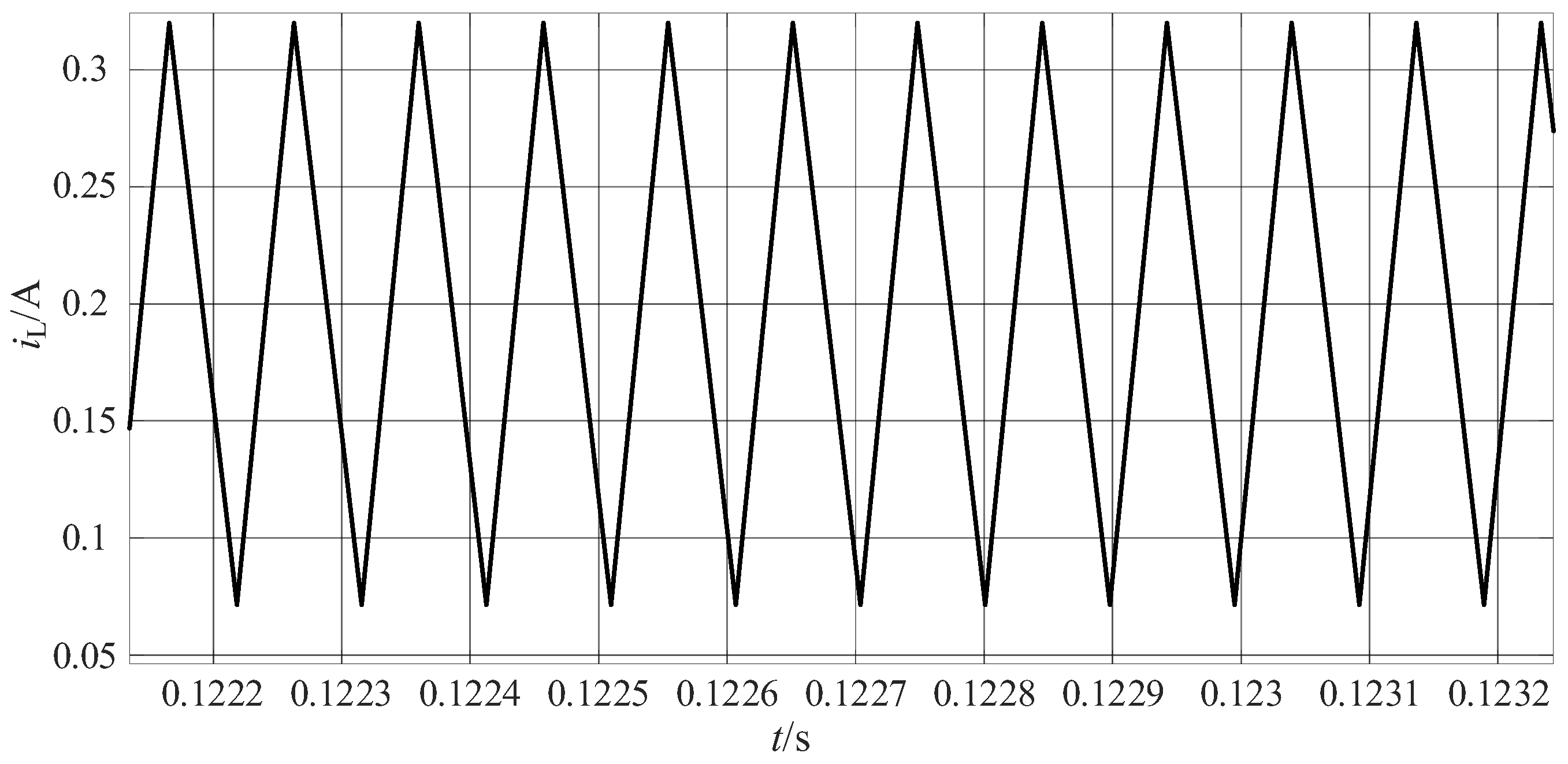
4.2. Reference Current Iref as the Bifurcation Parameter

With an input voltage Vin set to 12 V, the reference current Iref is selected as the perturbation parameter, while the remaining circuit parameters are detailed in Table 1. The bifurcation diagrams of the FO and IO converters are presented in Figure 10 and Figure 11, respectively.
Figure 10 illustrates that the FO flyback converter maintains stability when Iref is less than 0.299 A. At Iref = 0.299 A, the system undergoes its first period-doubling bifurcation. In the range of 0.299 A < Iref < 0.43 A, the converter operates in a period-2 state. When Iref exceeds 0.43 A, the system transitions into a chaotic state
Similarly, as shown in Figure 11, the IO converter operates stably when Iref is below 0.302 A. For 0.302 A < Iref < 0.46 A, the system exhibits period-2 behavior. Beyond Iref = 0.46 A, the system becomes chaotic.
The operating states of FO and IO flyback converters under different reference currents are shown in Table 4. Table 4 shows that, under the same parameter conditions, the stable operating regions of the FO converter and the IO converter are similar. However, when Iref = 0.43 A, the FO converter is in a chaotic operating state, while the IO converter enters into a chaotic operating state when Iref = 0.46 A.

4.3. FO of Inductance and Capacitance Is Used as the Bifurcation Parameter

Setting Vin = 12 V and Iref = 0.32 A, α = β, and the remaining circuit parameters are detailed in Table 1. Figure 12 illustrates the bifurcation diagram of the converter with respect to the fractional orders of inductance and capacitance.
When α = β < 0.86, the system maintains a stable operational condition. When 0.86 < α = β < 0.968, the system is in a binary bifurcation running state. When α = β > 0.968, the system enters the stable state again. In addition, it can be observed that the values of the output voltage uo and inductor current iL show different trends with the change of the order of inductor and capacitor. Therefore, the output voltage uo and inductor current iL of the flyback converter are related to the order of inductor and capacitor.

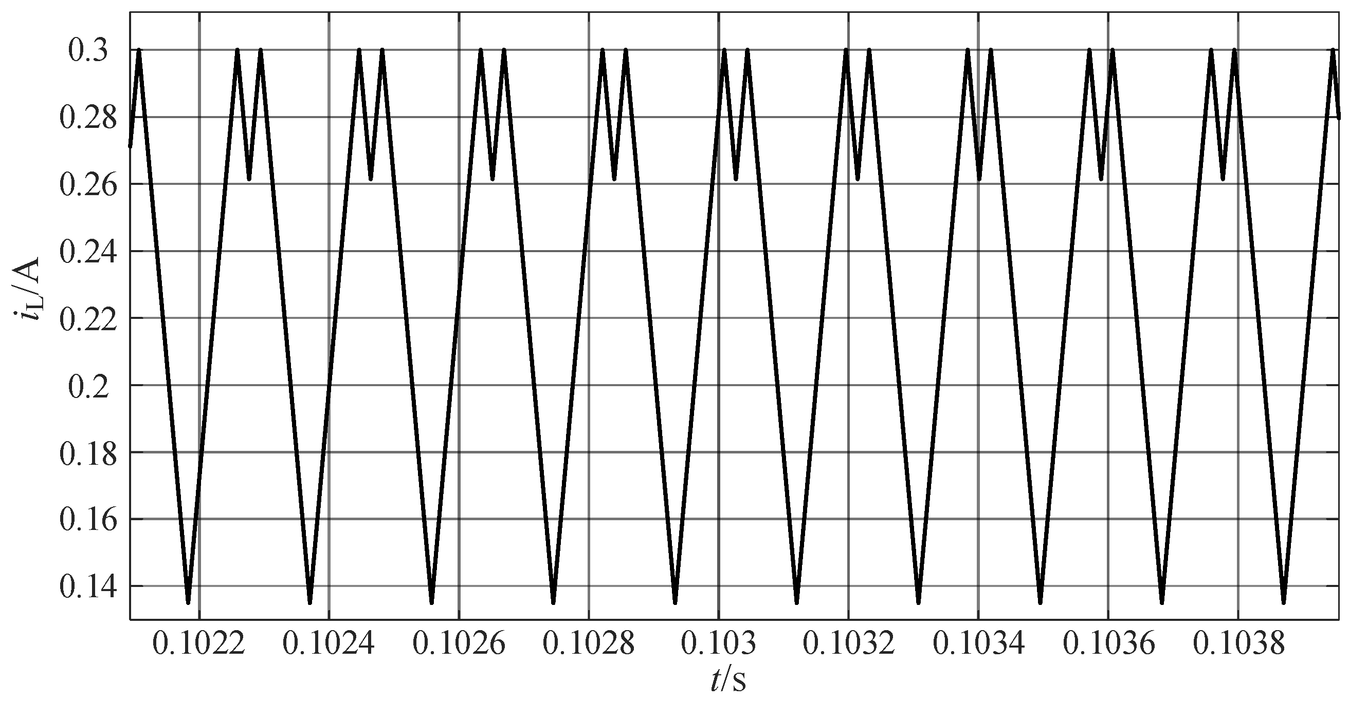
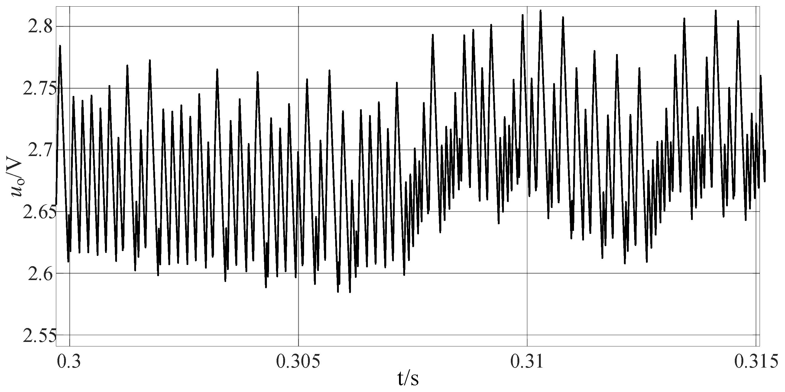
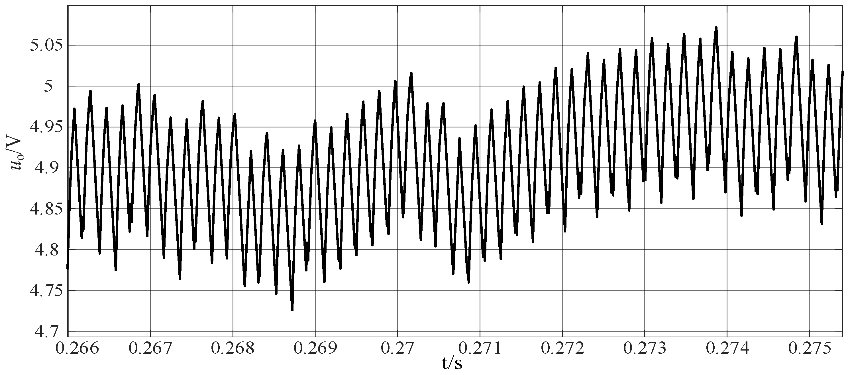
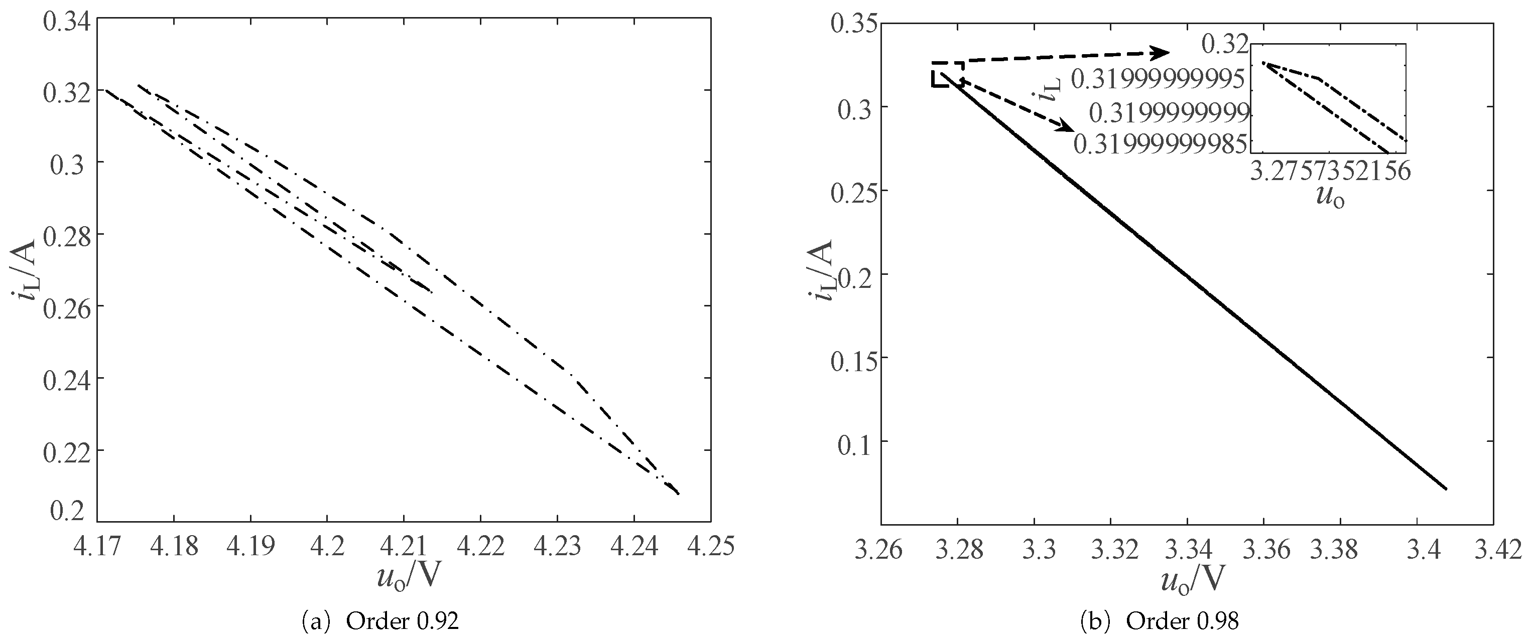
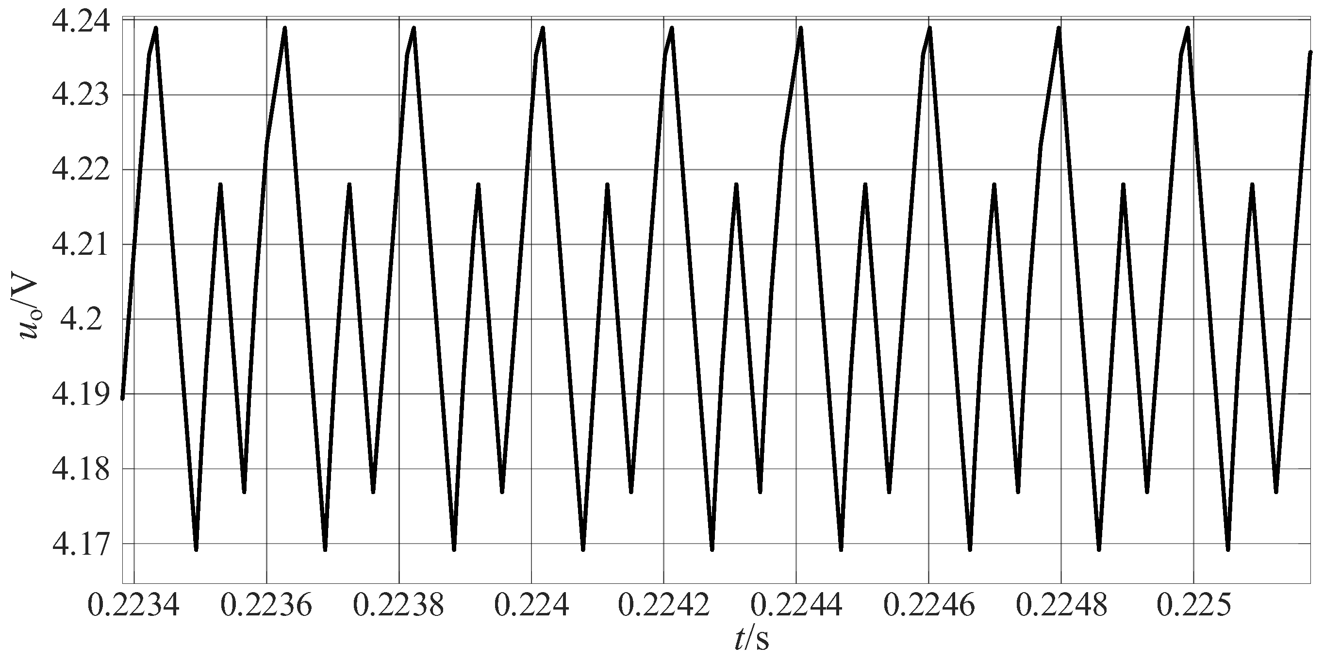
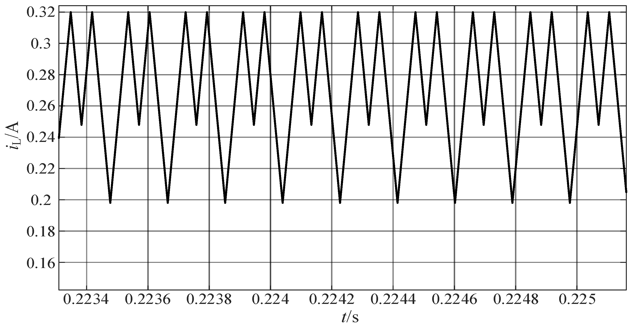
4.4. Phase Diagrams and Time-Domain Simulation Results

To validate the accuracy of the mathematical model, the parameters listed in Table 1 are incorporated into the simulation model depicted in Figure 5. When Iref = 0.3 A, the V–I phase diagrams of the converter for various input voltages Vin are depicted in Figure 13. Specifically, Figure 13a,b illustrate that when Vin = 11, the limit cycle of the phase diagram trajectory presents a double ring structure, indicating that the FO flyback converter is operating in period 2. When Vin = 9 V, the phase diagram of the FO flyback converter is chaotic, and the FO system can be determined to be in a chaotic state. When α = β = 1, the phase diagrams of the IO flyback converter are shown in Figure 13c,d. It can be observed that there is only one limit cycle when Vin = 11 V, meaning that the system is stable. When Vin = 9 V, an obvious depression appears, and the IO flyback converter is in the period-2 state. This aligns with the analytical findings depicted in Figure 8 and Figure 9. Figure 14, Figure 15, Figure 16 and Figure 17 depict the current and voltage waveforms of the flyback converter under the period-doubling bifurcation and chaotic states, respectively. These experimental results are consistent with the findings presented in Figure 12a,b.
When Vin = 10 V, the V–I phase diagram of the converter under different Iref is shown in Figure 18. As shown in Figure 18a,c, when Iref = 0.301 A, there is a depression in the limit cycle of the FO flyback converter, which divides the limit cycle into two parts, indicating that the FO system is operating in period-2. However, the phase diagram trajectory of the IO flyback converter system has only one limit cycle, which indicates that the IO flyback converter system is stable. Figure 18b,d show that when Iref = 0.45 A, the FO flyback converter operates in a state of chaos, while the IO flyback converter works in a period-2 state. These results are in agreement with the data analysis illustrated in Figure 10 and Figure 11. Figure 19, Figure 20, Figure 21 and Figure 22 present the current and voltage waveforms of the flyback converter under period-doubling bifurcation and chaotic states with the different values of the reference current. These results are consistent with the findings shown in Figure 18a,b.
The phase diagram of FO flyback converter with different orders of inductance and capacitance is shown in Figure 23. The current and voltage waveforms of the flyback converter under period-doubling bifurcation and stable states, with the fractional order as the bifurcation parameter, are depicted in Figure 24, Figure 25, Figure 26 and Figure 27.
Figure 23 shows that the system exhibits distinct dynamical behaviors at different fractional orders: a period-doubling bifurcation occurs when the inductance and capacitance orders are α = β = 0.92, while a stable state is achieved at α = β = 0.98. These observations are in complete agreement with the bifurcation characteristics presented in Figure 12. The waveforms shown in Figure 24, Figure 25, Figure 26 and Figure 27 exhibit strong agreement with the bifurcation characteristics previously established in Figure 23.

5. Conclusions

This study presents a comprehensive investigation into the nonlinear dynamics of a voltage-mode-controlled FO CCM flyback converter utilizing the GEM approach. Through systematic analysis employing bifurcation diagrams, V–I phase portraits, and simulated time domain diagrams, the research reveals complex nonlinear phenomena, including period-doubling bifurcation and chaotic behavior, which emerge under specific operational conditions characterized by particular reference current values, input voltage levels, and FO inductance/capacitance parameters. The principal findings can be summarized as follows:
(1) The FO flyback converter demonstrates extensive nonlinear characteristics that are significantly influenced by variations in reference current, input voltage, and the fractional orders of inductance and capacitance.
(2) Comparative analysis with integer-order (IO) converters indicates that the FO system exhibits period-doubling bifurcation at reduced parameter thresholds, suggesting a substantially narrower stability region compared to its IO counterpart.
(3) The FO model provides enhanced accuracy in characterizing converter dynamics as it more precisely represents the inherent fractional-order properties of practical inductors and capacitors. This improved modeling approach enables more reliable prediction and analysis of complex nonlinear phenomena, including bifurcation and chaotic behavior, under specific parametric conditions.
(4) The experimental results validate the methodological robustness and practical applicability of GEM for FO system analysis, establishing a theoretical foundation for its potential extension to other FO converter topologies.
Based on this study, future research may be extended to FO modeling and chaotic behavior mitigation in multiple converter topologies (e.g., Buck and Zeta configurations), incorporating AI-driven optimization algorithms to enhance adaptive control strategies. Additionally, exploring potential applications in high-efficiency energy storage systems and electric vehicle power supply architectures would represent a promising direction for industrial implementation.

Author Contributions

Project administration, L.X.; writing—original draft preparation, L.P. All authors have read and agreed to the published version of the manuscript.

Funding

This research was funded by National Natural Science Foundation of China, grant number 52377172.

Data Availability Statement

The data presented in this study are available on request from the corresponding author.

Conflicts of Interest

The authors declare no conflicts of interest. The funders had no role in the design of the study; in the collection, analyses, or interpretation of data; in the writing of the manuscript; or in the decision to publish the results.

Abbreviations

The following abbreviations are used in this manuscript:
FOfractional order
GEMgeneralized Euler method
IOinteger order
CCMcontinuous current mode

References

  1. Tushar, W.; Pradyumn, C. Sliding mode controller for multiphase bidirectional flyback converter topology in hybrid electric vehicle applications. Energy Rep. 2023, 9, 40–47. [Google Scholar]
  2. Ronilaya, F.; Djulihenanto, S.; Murdani, A.; Siradjuddin, I.; Rohadi, E.; Asmara, R.A.; Nurhadi, S. An improved control method to reduce harmonic level for a single phase grid-connected flyback micro-inverter of a small scale solar PV. J. Phys. Conf. Ser. 2019, 1402, 33098. [Google Scholar] [CrossRef]
  3. Benisha, S.; Roseline, J.A. Interleaved Boost Integrated Flyback Converter for Power Factor Correction in Brushless DC Motor Drive. Intell. Autom. Soft Comput. 2022, 33, 1363–1378. [Google Scholar] [CrossRef]
  4. S Zhou, G.Z.S.Z. Sampled-Data Modeling and Dynamic Behavior Analysis of Peak Current-Mode Controlled Flyback Converter with Ramp Compensation. J. Power Electron. 2019, 19, 190–200. [Google Scholar]
  5. Miklos, C.; Miklos, K. A Novel Feedback Linearisation Control of Flyback Converter. Power Electron. Drives 2023, 8, 74–83. [Google Scholar]
  6. Jesus, I.S.; Machado, J.A.T. Development of fractional order capacitors based on electrolyte processes. Nonlinear Dyn. 2009, 56, 45–55. [Google Scholar] [CrossRef]
  7. Monje, C.A.; Chen, Y.; Vinagre, B.M.; Xue, D.; Feliu-Batlle, V. Fractional-Order Systems and Controls: Fundamentals and Applications; Springer Science&Business Media: Berlin/Heidelberg, Germany, 2010. [Google Scholar]
  8. Allagui, A.; Freeborn, T.J.; Elwakil, A.S.; Fouda, M.E.; Maundy, B.J.; Radwan, A.G.; Said, Z.; Abdelkareem, M.A. Review of fractional-order electrical characterization of supercapacitors. J. Power Sources 2018, 400, 457–467. [Google Scholar] [CrossRef]
  9. Cao, W.; Chen, X. On the Influence of Fractional-Order Resonant Capacitors on Zero-Voltage-Switching Quasi-Resonant Converters. Electronics 2024, 13, 2562. [Google Scholar] [CrossRef]
  10. Yu, D.; Liao, X.; Wang, Y. Modeling and Analysis of Caputo–Fabrizio Definition-Based Fractional-Order Boost Converter with Inductive Loads. Fractal Fract. 2024, 8, 81. [Google Scholar] [CrossRef]
  11. Jiang, X.; Chen, Y.; Zhang, B.; Qiu, D. Transient modeling and analysis of fractional-order resonant very high frequency boost converter. Compel-Int. J. Comp. Math. Electr. Electron. Eng. 2022, 41, 1428–1449. [Google Scholar] [CrossRef]
  12. Xie, L.; Shi, J.; Yao, J.; Wan, D. Research on the Period-Doubling Bifurcation of Fractional-Order DCM Buck–Boost Converter Based on Predictor-Corrector Algorithm. Mathematics 2022, 10, 1993. [Google Scholar] [CrossRef]
  13. Wang, X.; Zhang, Z.; Chen, Y. Fractional-order modeling and nonlinear dynamics analysis of voltage mode controlled flyback converter. Nonlinear Dyn. 2024, 112, 21471–21490. [Google Scholar] [CrossRef]
  14. Zirui, J.; Ling, L.; Chongxin, L. Dynamic Analysis and Fractional-Order Terminal Sliding Mode Control of a Frac-tional-Order Buck Converter Operating in Discontinuous Conduction Mode. Int. J. Bifurc. Chaos 2022, 32, 2250045. [Google Scholar]
  15. Liao, X.; Wang, Y.; Yu, D.; Lin, D.; Ran, M.; Ruan, P. Modeling and analysis of Buck-Boost converter with non-singular fractional derivatives. Chaos Solitons Fractals Interdiscip. J. Nonlinear Sci. Nonequilibrium Complex Phenom. 2023, 169, 113336. [Google Scholar] [CrossRef]
  16. Odibat, Z.M.; Momani, S. An algorithm for the numerical solution of differential equations of fractional order. J. Appl. Math. Inform. 2008, 26, 15–27. [Google Scholar]
  17. Diethelm, K.; Ford, N.J.; Freed, A.D. A Predictor-Corrector Approach for the Numerical Solution of Fractional Differential Equations. Nonlinear Dyn. 2002, 29, 3–22. [Google Scholar] [CrossRef]
  18. Li, C.; Zhao, Z.; Chen, Y. Numerical approximation of nonlinear fractional differential equations with subdiffusion and superdiffusion. Comput. Math. Appl. 2011, 62, 855–875. [Google Scholar] [CrossRef]
  19. Zhang, Y.; Li, Y.; Yu, Y.; Wang, W. Implicit Runge-Kutta with spectral Galerkin methods for the fractional diffusion equation with spectral fractional Laplacian. Numer. Meth. Part Differ. Equ. 2023, 40, e23074. [Google Scholar] [CrossRef]
  20. Gu, B.; Zhang, S.; Liu, X.; Han, J. Efficient modeling of fractional Laplacian viscoacoustic wave equation with fractional finite-difference method. Comput. Geosci. 2024, 191, 105660. [Google Scholar] [CrossRef]
  21. Arafa, A.A.M.; Rida, S.Z.; Khalil, M. A fractional-order model of HIV infection: Numerical solution and comparisons with data of patients. Int. J. Biomath. 2014, 7, 1450036. [Google Scholar] [CrossRef]
  22. Priya, P.; Sabarmathi, A. Caputo Fractal Fractional Order Derivative of Soil Pollution Model Due to Industrial and Agrochemical. Int. J. Appl. Comput. Math. 2022, 8, 250. [Google Scholar] [CrossRef] [PubMed]
  23. Odibat, Z.M.; Shawagfeh, N.T. Generalized Taylor’s formula. Appl. Math. Comput. 2006, 186, 286–293. [Google Scholar] [CrossRef]
  24. Wang, F.Q.; Ma, X.K. Transfer function modeling and analysis of the open-loop Buck converter using the fractional calculus. Chin. Phys. B 2013, 22, 30506. [Google Scholar] [CrossRef]
Figure 1. FO flyback converter with peak current control.
Electronics 14 00977 g001
Figure 2. Topology diagram of working mode 1.
Electronics 14 00977 g002
Figure 3. Topology diagram of working mode 2.
Electronics 14 00977 g003
Figure 4. Mathematical model of flyback converter.
Electronics 14 00977 g004
Figure 5. Simulation model of FO flyback converter.
Electronics 14 00977 g005
Figure 6. 0.9 fractional-order equivalent inductance.
Electronics 14 00977 g006
Figure 7. 0.9 fractional-order equivalent capacitance.
Electronics 14 00977 g007
Figure 8. Bifurcation characteristics of the FO converter with Vin as the controlling parameter.
Electronics 14 00977 g008
Figure 9. Bifurcation diagram of IO converter using Vin as bifurcation parameter.
Electronics 14 00977 g009
Figure 10. Bifurcation diagram of FO converter using Iref as bifurcation parameter.
Electronics 14 00977 g010
Figure 11. Bifurcation diagram of IO converter with Iref as bifurcation parameter.
Electronics 14 00977 g011
Figure 12. Bifurcation diagram using α and β as bifurcation parameters.
Electronics 14 00977 g012
Figure 13. Flyback converter V–I phase diagram at different input voltages.
Electronics 14 00977 g013
Figure 14. Waveform diagram of the period-doubling bifurcation voltage in the flyback converter with input voltage Vin = 11 V.
Electronics 14 00977 g014
Figure 15. Waveform diagram of the period-doubling bifurcation current in the flyback converter with input voltage Vin = 11 V.
Electronics 14 00977 g015
Figure 16. Waveform diagram of the chaotic voltage in the flyback converter with input voltage Vin = 9 V.
Electronics 14 00977 g016
Figure 17. Waveform diagram of the chaotic current in the flyback converter with input voltage Vin = 9 V.
Electronics 14 00977 g017
Figure 18. Flyback converter V–I phase diagram with different reference currents.
Electronics 14 00977 g018
Figure 19. Waveform diagram of the period-doubling bifurcation voltage in the flyback converter with reference current Iref = 0.301 A.
Electronics 14 00977 g019
Figure 20. Waveform diagram of the period-doubling bifurcation current in the flyback converter with reference current Iref = 0.301 A.
Electronics 14 00977 g020
Figure 21. Waveform diagram of the chaotic voltage in the flyback converter with reference current Iref = 0.45 A.
Electronics 14 00977 g021
Figure 22. Waveform diagram of the chaotic current in the flyback converter with reference current Iref = 0.45 A.
Electronics 14 00977 g022
Figure 23. Phase diagram of FO flyback converter with different fractional order.
Electronics 14 00977 g023
Figure 24. Waveform diagram of the period-doubling bifurcation voltage in the flyback converter with the fractional order α = β = 0.92.
Electronics 14 00977 g024
Figure 25. Waveform diagram of the period-doubling bifurcation current in the flyback converter with the fractional order α = β = 0.92.
Electronics 14 00977 g025
Figure 26. Waveform diagram of the stable voltage in the flyback converter with the fractional order α = β = 0.98.
Electronics 14 00977 g026
Figure 27. Waveform diagram of the stable current in the flyback converter with the fractional order α = β = 0.98.
Electronics 14 00977 g027
Table 1. The circuit parameters.
Circuit ComponentsValues
Input voltage (Vin)12 V
ratio of transformer3
Inductor (L)2 mH
Capacitor (C)100 μF
Inductance order (α)0.9
Capacitance order (β)0.9
Switching frequency10 kHz
Resistor (R)10.5 Ω
Reference current (Iref)0.3 A
Table 2. Resonant converter parameters.
L = 2 × 10⁻⁴ HC = 1 × 10⁻⁶ F
α = 0.9β = 0.9
iRLi (Ω)Li (H)RCi (Ω)Ci (F)
1043.998 m22.390
2386.418 k18.208 m20.000 m4.720 m
3162.29235.904 m15.3206.164 m
4320 m14.624 m11.817 k7.990 m
51303.07628.758 m1.7195.489 m
62.56812.492 m1.234 k7.652 m
711.132 k22.568 m0.1904.969 m
820.51640 m0.137 k6.868 m
936.908 m0878.279 k1.075 m
Table 3. The range of input voltage values for the FO and IO CCM flyback converters.
Type of ConverterStable RegionPeriod-2 RegionChaotic Region
FO flyback11.9 V~15 V10.16 V~11.9 V0 V~10.16 V
IO flyback9.76 V~15 V8.65 V~9.76 V0 V~8.65 V
Table 4. Reference current value range of FO and IO CCM flyback converter.
Type of ConverterStable RegionPeriod-2 RegionChaotic Region
FO flyback0 A~0.299 A0.299 A~0.43 A0.43 A~1 A
IO flyback0 A~0.302 A0.302 A~0.46 A0.46 A~1 A
Disclaimer/Publisher’s Note: The statements, opinions and data contained in all publications are solely those of the individual author(s) and contributor(s) and not of MDPI and/or the editor(s). MDPI and/or the editor(s) disclaim responsibility for any injury to people or property resulting from any ideas, methods, instructions or products referred to in the content.

