Article

A Wideband Analog Vector Modulator Phase Shifter Based on Non-Quadrature Vector Operation

1
School of Electrical Engineering and Computer Science, University of Ottawa, Ottawa, ON K1N 6N5, Canada
2
Department of Electronics, Carleton University, Ottawa, ON K1S 5B6, Canada
*
Author to whom correspondence should be addressed.
Electronics 2025, 14(5), 997; https://doi.org/10.3390/electronics14050997
Submission received: 8 February 2025 / Revised: 27 February 2025 / Accepted: 28 February 2025 / Published: 28 February 2025
(This article belongs to the Special Issue Advanced RF/Microwave Circuits and System for New Applications)

Abstract

:
Phase shifters are essential components of phased array systems, which are crucial to radar and wireless communication systems. New-generation telecommunication and radar systems often require strict phase shifter performance metrics, such as phase resolution and bandwidth, to perform fine beam scanning, which helps increase pointing accuracy. Meanwhile, practical vector modulator phase shifters, which employ quadrature signal operation, typically have digital control below 7 bits. In this regard, a vector modulator phase shifter based on non-quadrature signal operation and covering the lower S-band and upper C-band is proposed and implemented in this work. The proof-of-concept printed circuit board (PCB) prototype exhibits more than 360° continuous phase shift with more than 50% fractional bandwidth. In addition, it achieves a median gain of 0.8 dB and a size of 0.9 λ g 2 with the inclusion of an output gain-block amplifier. The relatively wider bandwidth, smaller size, and fine resolution of the proposed phase shifter approach make it a potential candidate for new-generation ultrawideband communication and radar systems.

1. Introduction

Antenna array techniques have been the most preferred beam steering methods for diverse applications, including military surveillance and wireless communications, due to their higher signal-to-noise ratio (SNR) and signal-to-interference ratio (SIR) as well as faster scanning speed. Particularly, the recent development of the fifth generation (5G) telecommunication and high-throughput satellite systems leads to an ever-growing demand for high-performant phased array systems operating in the millimeter-wave frequencies [1,2]. Phase shifters are an integral part of antenna array beamformers alongside antenna elements. Nevertheless, implementing precise and low-resolution phase shifters generally requires a costly process, substantially increasing the overall cost of the system, which is typically composed of dozens of array elements. In this regard, the design of high-performance phase shifters using cost-effective processes has been explored in the literature. High linearity and low power consumption may be achieved by passive phase shifters such as the switched-type phase shifters (STPSs) [3,4,5] and the reflective-type phase shifters (RTPSs) [6,7,8]. However, passive phase shifters typically exhibit lower phase resolution and system gain in addition to their large areas. On the other hand, vector-sum phase shifters (VSPS) or vector modulators offer higher gain and are relatively more compact than their passive counterparts [9,10,11,12,13,14,15,16,17,18]. Conventional vector modulators are based on the generation and synthesis of balanced in-phase (I) and quadrature (Q) signals, which is challenging. Differential I/Q signals may be generated using polyphase filters (PPFs) [9]. Nevertheless, RC PPFs detain a higher insertion loss, limiting their operation for lower gigahertz frequencies. The insertion loss may be reduced by using the current-mode RC PPF design [12] but at the cost of a larger area and higher power consumption. Moreover, quadrature all-pass filters (QAFs) are often employed to generate balanced I/Q signals. In contrast, QAFs suffer from amplitude and phase mismatches when loaded by the capacitive input of the variable-gain amplifier (VGA), which it typically precedes. As a result, techniques such as inductive loading [13,14] and series resistance [15,16] are used to alleviate the capacitive loading effect at the expense of lower system gain. In addition, generating differential I/Q signals through PPFs and QAFs requires an input balun, further increasing the chip area of the phase shifter. Despite the difficulty of generating area-effective I/Q signals, the generated balanced signals are typically subjected to phase-invertible VGAs, which may be implemented with at least two differential amplifiers [11,15,16] or four or more single-ended amplifiers [9,12,17]. Consequently, the power overhead of traditional quadrature vector modulators is relatively high. Moreover, it is desired for the phase shifter to provide close to fine resolution (e.g., 1°) to reduce quantization errors and significant beam sidelobes [18]. Meanwhile, vector modulators present “phase gaps” between quadrants, thereby limiting their resolution [11]. For that reason, most reported VSPSs operate under 7-bit digital control. An analog resolution was achieved in [10] using a passive vector modulator. Nevertheless, the total phase range obtained is below 360°. In addition to their limited resolution, most reported phase shifters do not operate beyond 25% fractional bandwidth (FBW). On that account, a novel VSPS based on non-quadrature vector generation and synthesis is proposed and implemented in this work to address the phase range/resolution limitation issue while operating at a wide frequency band.
The remaining part of the article is organized as follows: Section 2 and Section 3 provide the generalized principle of the proposed vector modulator and the implementation of its building blocks on PCB, respectively. Section 4 discusses the results obtained from the fabricated PCB and compares them to selected relevant works. Finally, Section 5 summarizes the work.

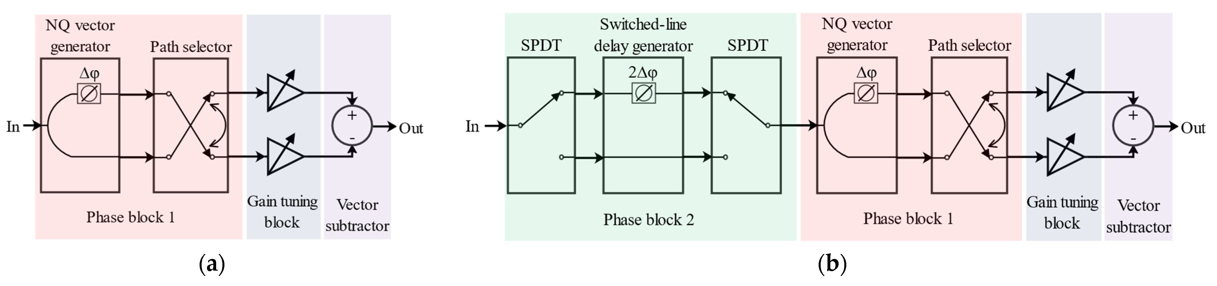
2. Conceptual Block Diagram of the Non-Quadrature Vector Modulator

The basic block diagram of the proposed non-quadrature (NQ) vector modulator is represented in Figure 1a. It consists of an NQ vector generator with path selection (Phase block 1), a gain variation unit composed of two VGAs (or attenuators), and a vector subtractor. Two RF signals with a phase difference φ < 90 ° are generated by phase block 1 and subjected to gain variation before synthesis by the subtractor. The output phase variation is executed based on the arctangent operation, as demonstrated by the phase φ P S and gain A P S expressions of the modulator expressed below:
φ P S = tan 1 A V G A 2 sin ( φ ) A V G A 2 cos ( φ ) A V G A 1 , f o r   A V G A 2 cos ( φ ) A V G A 1 180 + tan 1 A V G A 2 sin ( φ ) A V G A 2 cos ( φ ) A V G A 1 ,   f o r   A V G A 2 cos ( φ ) < A V G A 1 ,
A P S = A V G A 2 2 + A V G A 1 2 2 A V G A 2 A V G A 1 cos φ ,
where A V G A 1 and A V G A 2 are the gains (or attenuations) of the two VGAs (or attenuators) and φ the NQ phase difference generated by phase block 1. To obtain the maximum system gain and minimum gain imbalance in a vector modulator phase shifter, the gain of one of the VGAs must be maintained at the maximum gain state (e.g., A V G A 1 = A V G A , m a x ), while the other is tuned between the minimum and maximum gain states (e.g., A V G A 2 = A ∈ [ A V G A , m i n , A V G A , m a x ]). In this regard, the minimum and maximum system phase shift and gain can be obtained using (1) and (2) as tan 1 sin ( φ ) cos φ A V G A , m i n A V G A , m a x and 180 ° tan 1 sin φ A V G A , m a x A V G A , m i n cos φ , respectively, leading to the system phase and gain ranges for all phase states in a 2-quadrant operation, expressed as follows:
φ P S , r a n g e = 2 180 ° tan 1 sin φ A V G A , r a n g e cos φ tan 1 sin ( φ ) cos φ 1 / A V G A , r a n g e ,
A P S , r a n g e = A P S , m a x A P S , m i n = 1 + A V G A , r a n g e 2 2 A V G A , r a n g e cos φ sin φ ,
where A P S , m a x , and A P S , m i n are the maximum and minimum gains of the phase shifter, respectively, and A V G A , r a n g e = A V G A , m a x A V G A , m i n , the gain tuning range of the VGAs. The generation of a 360° phase range is challenging with a 2-quadrant operation [19]. To achieve a 360° continuous phase shift, the addition of Phase block 2 with a minimum phase difference of 2 φ is necessary, as depicted in Figure 1b, thus leading to a 4-quadrant phase tuning. In addition, the VGA or attenuator gain range requirement is reduced. For instance, if φ = 45 ° , each quadrant must generate 90° to obtain a 360° phase range. In this respect, the required VGA gain can be found by equating the 2-quadrant phase range in (3) to 2 × 90°, resulting in A V G A , r a n g e = 7.6 dB (only). Therefore, the required VGA gain range is only 7.6 dB. If properly designed, the proposed modulator has the advantage of a reduced area compared to a conventional quadrature modulator since the phase shift of a transmission line is proportional to its size. In addition, the two-branch vector operation of the NQ modulator potentially results in lower power consumption than the traditional differential quadrature vectors.

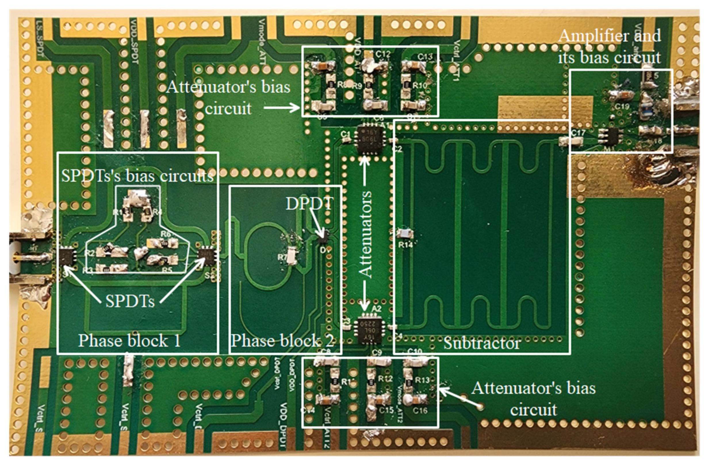
3. Implementation of the Proposed Phase Shifter
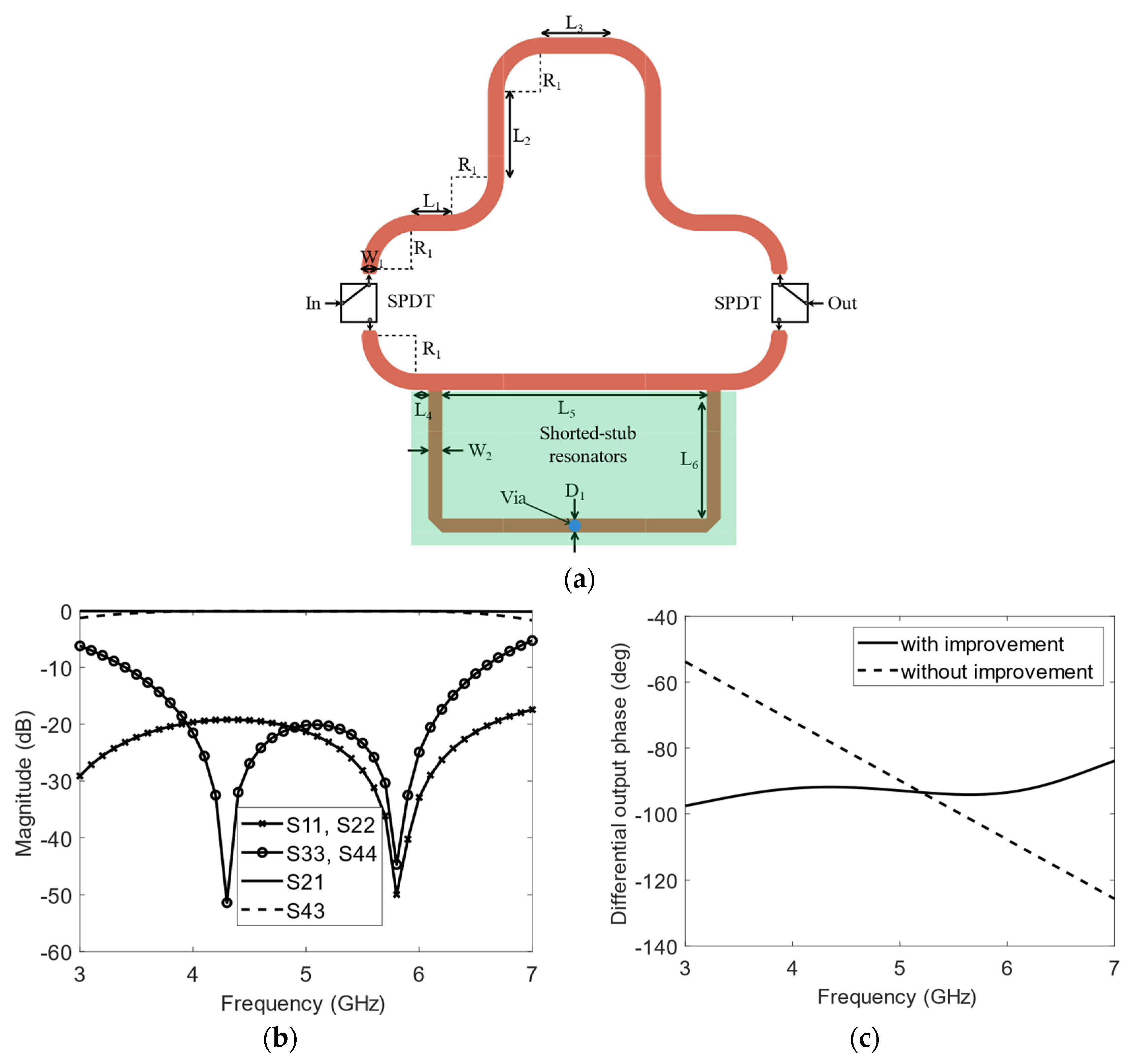
This section describes a proof-of-concept printed circuit board (PCB) implementation. Table 1 provides the general design target parameters. This practice intends to use a center frequency of 5 GHz with a minimum FBW of 40% and at least 0 dB average gain with a maximum gain imbalance of 4 dB.
The substrate used is RT/Duroid 5880 with thickness h = 0.252 mm, dielectric constant ϵ r = 2.2 , and loss tangent tan δ = 0.0019 .

3.1. Phase Block 1

It is intended to generate a φ = 45 ° at a center frequency of f 0 = 5 GHz. This may be achieved through a power divider with an output length difference of an eighth wavelength ( λ 0 / 8 ). However, using the substrate described earlier, this generates a total phase variation of about ±9° between 4 GHz and 6 GHz. To reduce the phase variation, a half-wavelength ( λ 0 / 2 ) open-stub T-resonator may be incorporated at the shorter output line of the splitter, as seen in Figure 2a, which describes the NQ vector generator and its path selector. Highlighted in green, the stub creates a slow-wave effect at frequencies adjacent to the center frequency. As demonstrated in [20], the T-resonator acts as a bandpass filter with bandwidth controlled by the characteristic impedance of its tail. In this regard, the phase variation decreases as the tail impedance decreases, leading to a decreasing frequency bandwidth. Nevertheless, an optimum impedance value may be obtained by tuning the width of the resonator tail. The optimum dimensions of the proposed NQ vector generator described in Figure 2a are summarized in Table 2. The structure is simulated in the Keysight-ADS momentum environment, and the scattering parameter (S-parameter) simulation results are illustrated in Figure 2b,c. The proposed vector generator achieved insertion and return losses below 3.43 and 13 dB between 4 GHz and 6.5 GHz, respectively, as illustrated in Figure 2b. This corresponds to a total loss of about 0.42 dB. To illustrate the phase variation improvement of the proposed wide phase bandwidth vector generator, an identical design without the open-stub section was simulated, and its output phase difference was plotted alongside that of the proposed design in Figure 2c. Total phase variations of 4° and 22° between 4 GHz and 6.5 GHz for the generators with and without the open-stub T-resonator were obtained, respectively. Thus, the proposed vector generator achieves a phase variation reduction of 81.8%. Maintaining a low variation of φ over a wide frequency range helps reduce changes in both the gain and phase of the modulator, as demonstrated by (3) and (4). This, in turn, leads to an improvement of the bandwidth over which uniform phase and gain ranges are obtained for a fixed VGA gain range.
To implement the vector generator’s isolation for proper input and output matching, a 100 Ω commercial RF resistor is selected [21]. Moreover, the path selector of phase block 1 is implemented using a commercial DPDT (BGSX22G6U10 from Infineon (Neubiberg, Germany)), with a maximum insertion loss of 0.95 dB, a minimum isolation of 19 dB, and a minimum return loss of 12 dB from 4 GHz to 6 GHz [22].

3.2. Phase Block 2

Phase block 2 is essentially a single-stage switched-line phase shifter (SLPS) with phase variation improvement, as seen in Figure 3a. The targeted output phase difference is 2 φ = 90 ° , which results in a reduced gain imbalance and an identical phase tuning range in each quadrant. Two shorted-stub T-resonators separated by a quarter-wavelength line are added at the ends of the shorter line to provide a slow-wave effect, similar to the open stub resonator previously discussed. Each stub has a length of λ 0 / 4 , generating a total delay of approximately 180° at frequencies adjacent to the center frequency, f0. Like their half-wavelength open-stub counterpart, the quarter-wavelength shorted stub resonators act as bandpass filter delay generators [20]. The optimum line dimensions of the proposed wideband switched-line phase block are provided in Table 3. The shorted stub T-resonators section is shaded in green. Figure 3b,c represent the ADS Momentum simulation results. A maximum insertion loss and minimum return loss of 0.43 dB and 11.1 dB are obtained between 3.5 GHz and 6.5 GHz, respectively, as demonstrated by Figure 3b. Furthermore, an identical conventional SLPS was simulated and compared with the proposed design. A total phase variation of only 4.6° was obtained for the proposed wideband switched-line delay block, whereas that of the conventional structure is 51.1° for the same bandwidth. This corresponds to a phase variation improvement of 91%.
Meanwhile, the path switching of Phase block 2 is realized using two single-pole double-throw (SPDT) switches. The discrete component switches are commercial (F2976NEGK8 from Renesas (Tokyo, Japan)) and exhibit a maximum insertion loss of 0.43 dB, a minimum isolation of 40 dB, and a typical return loss below 20 dB from 4 GHz to 6 GHz [23].

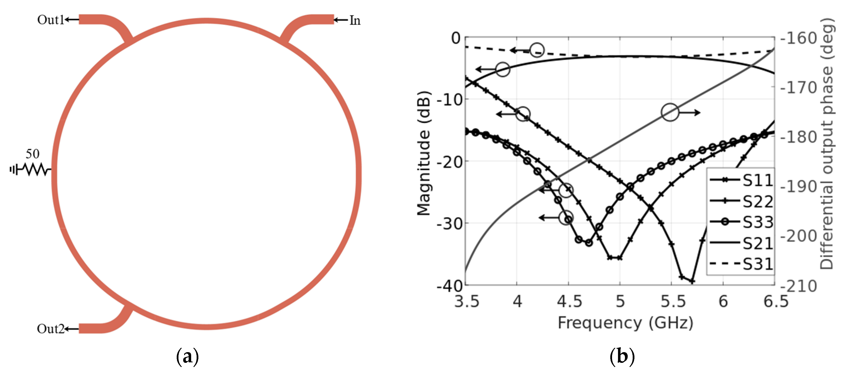
3.3. Vector Subtractor

After the generation of the NQ vectors, a synthesizer is required to generate the single-ended output signal. A vector subtractor is needed as an operator to obtain a wide phase tuning range. One way of subtracting analog vectors is through the 180° hybrid coupler, which has a coupling factor of 3 dB. An example of such a coupler is the conventional microstrip rat-race coupler, as represented in Figure 4a. The simulation results of a microstrip rat-race balun designed at 5 GHz center frequency using the laminate described earlier are provided in Figure 4b. One may observe from the figure that the phase difference between the output ports is about 180° at the center frequency. This phase difference changes at a rate of 12°/GHz as we move away from the center frequency between 4 GHz and 6 GHz. This high phase variation causes a reduction in the bandwidth of the phase shifter. Additionally, the gain mismatch increases as the frequency approaches 4 GHz and 6 GHz from the center. This mismatch results in phase and gain errors at the output if the phase shifter is digitally tuned. Furthermore, it leads to an increase in the gain imbalance of the phase shifter. For these reasons, an analog subtractor with a balanced insertion loss was proposed in this work, as illustrated in Figure 5a, which represents its conceptual schematic. The subtractor uses T-resonators in conjunction with balance-to-unbalance transformation to subtract two analog input signals. With a resistive isolation midway between the differential ports, the proposed subtractor may be used as a signal subtractor, where the inputs are port 2 and 3 and the output is port 1, as well as a single-to-differential converter, where the input is port 1 and the differential outputs are ports 2 and 3. As the frequency of operation moves from f0, more signals start to flow in the two center stubs, especially following the path from port 1 to port 2 since it offers the shortest path to the stubs. Consequently, the signal delay from port 1 to port 2 and port 1 to port 3 are compensated, and the phase difference between the output ports is maintained at 180°. Moreover, since the signal flowing in each path follows more or less the same path, including the center stubs, the insertion losses from port 1 to port 2 and from port 1 to port 3 are matched for a relatively wider range of frequencies compared to the conventional rat-race balun. The characteristic impedance ZT of the two middle stubs can be tuned to obtain the desired phase bandwidth or phase flatness by compromising the matching bandwidth of the input port. The proposed analog subtractor was designed and simulated using the Keysight ADS Momentum for a center frequency of 5 GHz. The substrate used is the RT/Duroid 5880 laminate previously described. Table 4 contains the subtractor’s optimized dimensions, illustrated in Figure 5b. The scattering parameter simulation results are given in Figure 5c. From the results, the proposed analog subtractor detains a return loss below 10 dB for ports 2 and 3 between 4 and 6 GHz. Therefore, a wideband operation with a low return loss is achieved in the signal subtraction mode. The insertion losses are also matched between 4 GHz and 6 GHz and vary from 3.2 dB to 4.2 dB. Thus, a maximum loss of about 1.19 dB is obtained within the desired bandwidth. Lastly, a variation of only 2.2° is obtained for the differential output phase between 4 GHz and 6 GHz.
A commercial high-frequency resistor (CH0603-50RJNT from Vishay (Malvern, PA, USA)) is used as the 50 Ω isolation for the subtractor/unbalance-to-balance converter [24].

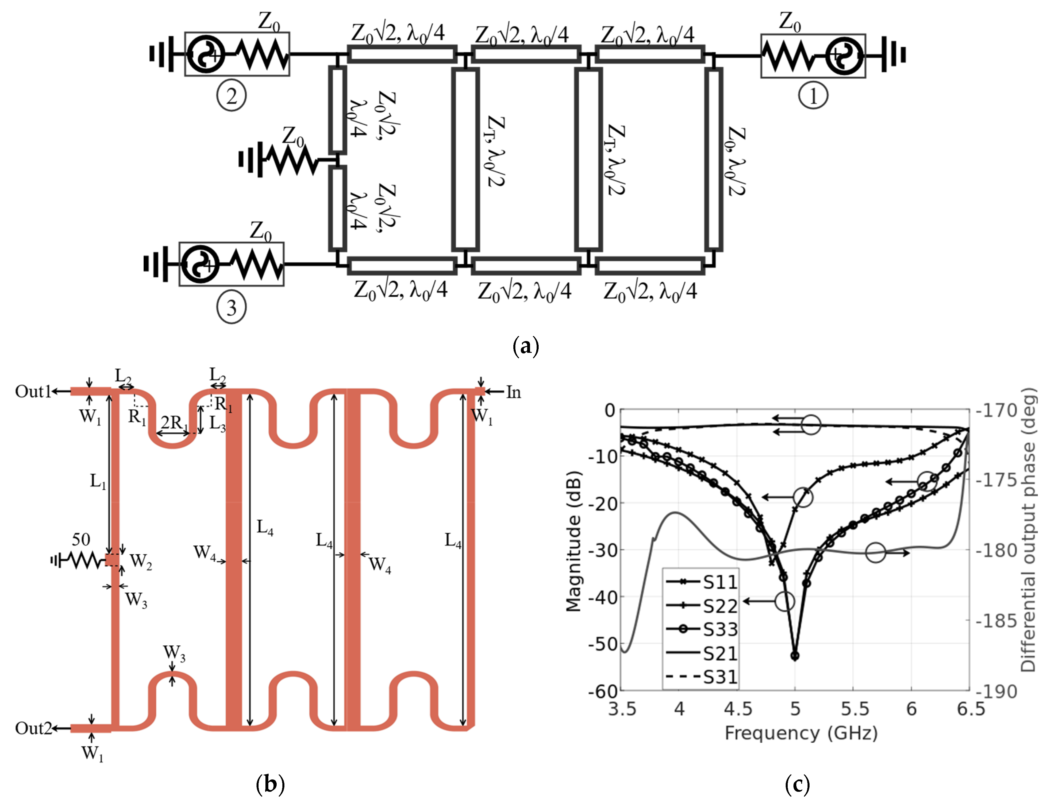
3.4. Gain-Tuning Block and Output Amplification

Attenuators are selected in this practice to perform fine-tuning. Attenuators offer several advantages over VGAs, including their broader availability in the market, relatively simpler biasing, and lower power consumption. Conversely, the use of attenuators as gain-tuning elements inevitably drops the system gain below 0 dB. Nevertheless, a gain-block amplifier may be used to boost the output signal. Employing 2 attenuators and an output amplifier offers lower power consumption and better linearity than 2 VGAs in the vector modulator. As previously stated, a minimum of 7.6 dB tuning range is required to obtain a 360° phase range for φ = 45 ° . The corresponding theoretical gain imbalance can be obtained from (4) as 1.4 dB. The low gain-tuning range allows for a wide range of low-cost discrete attenuators suitable for the design. To this end, a commercial attenuator (F2250NLGK8 from Renesas) with an insertion loss of 2.6 dB and a return loss above 11 dB between 4 GHz and 6 GHz is selected [25]. As indicated previously, the maximum losses produced by the NQ generator, the DPDT, the 90° delay block, the SPDTs, and the analog subtractor are 0.42 dB, 0.95 dB, 0.43 dB, 0.43 dB, and 1.19 dB, respectively. Assuming an 8 dB attenuator tuning, the maximum loss produced by tuning the attenuators is estimated at 11.2 dB. Consequently, the overall worst-case scenario loss produced by the system before gain boosting is estimated at 14.62 dB and sets the minimum gain requirement of the output amplifier. Accordingly, a commercial amplification device (TQP369184 from Qorvo (Greensboro, NC, USA)) with a gain ranging from 15 dB to 19 dB between 4 GHz and 6 GHz [26] is selected as it best fulfills the gain and bandwidth requirements of the proof-of-concept NQ vector modulator. Additionally, its typical input 1-dB compression point (P1dB,in), output third-order intercept point (OIP3), and noise figure (NF) are 11.4 dBm, 23.4 dBm, and 4.2 dB, respectively.

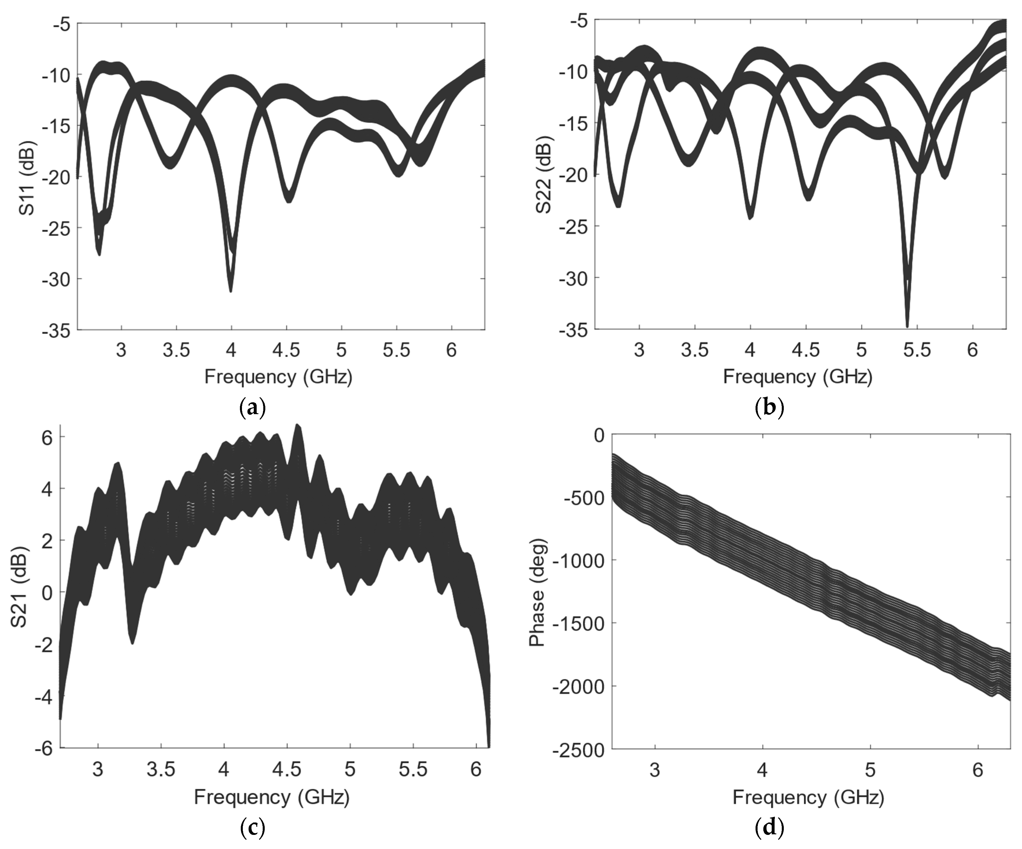
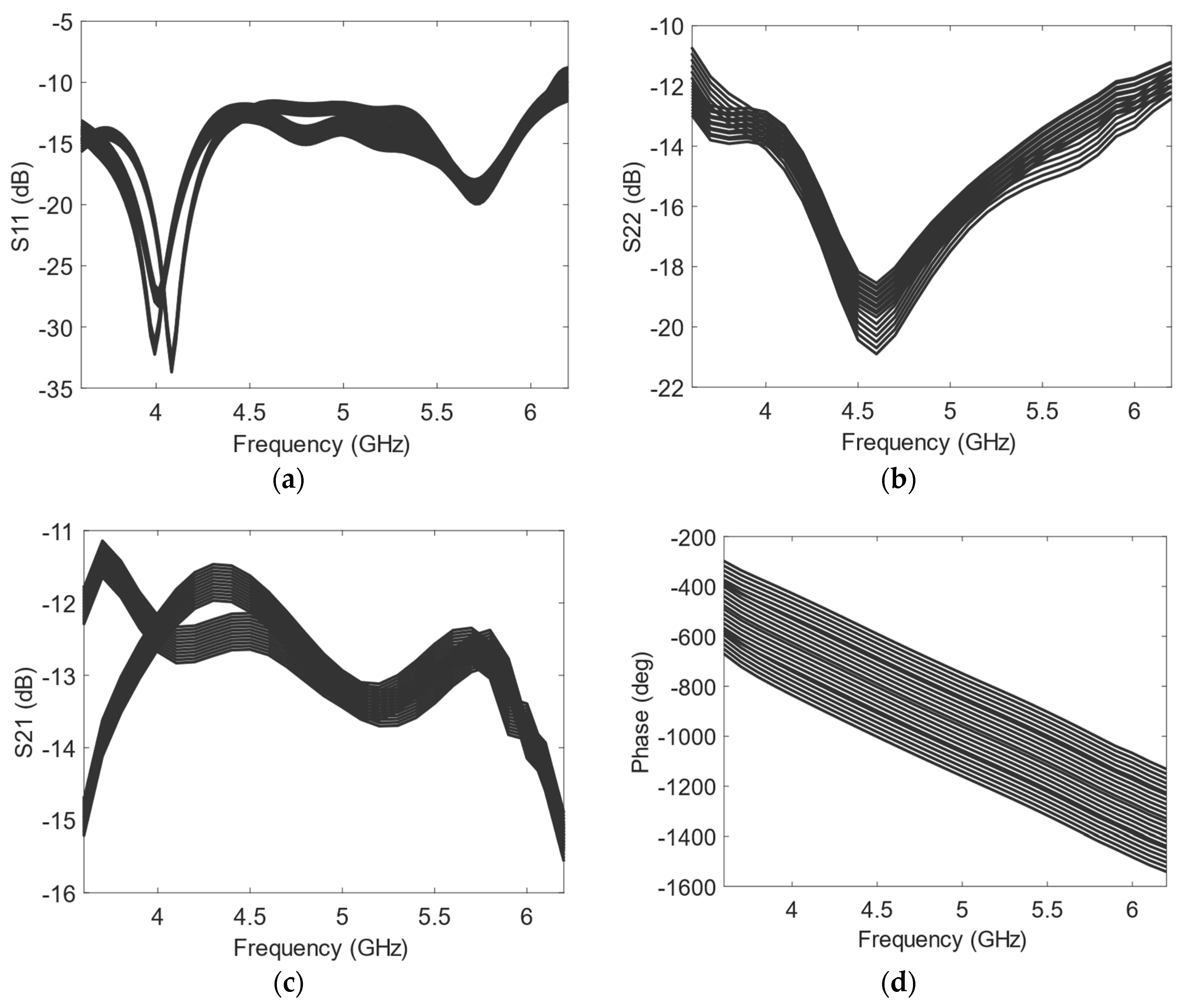
4. Measurement Results and Discussion

The constituent blocks of the proposed NQ vector modulator were combined and laid out on the RT/Duroid 5880 substrate. The fabricated PCB prototype is illustrated and labeled in Figure 6 and measures 83.1 × 53.5 mm2. It is worth noting, however, that the dimension of the phase shifter without the bias circuitry extensions is around 83.1 × 28 mm2. A bias variation from 0 to 1 V of the F2250NLGK8 attenuator generates a total attenuation of about 8 dB with a 4 V DC supply. In this regard, to achieve a full-quadrant phase tuning with minimal insertion loss, the control voltage of one of the attenuators is set to 0 while that of the other is tuned between 0 and 1 V in a negative slope tuning process. The scattering parameters are measured with six tuning states for each quadrant, generating a total of 24 measurements. Figure 7a,b represent the input and output reflection coefficients of the NQ modulator, respectively. It can be observed that the minimum input and output return losses obtained for the 4-quadrant operation are 10.6 dB and 7.5 dB, respectively, between 2.7 GHz and 6.1 GHz. Moreover, the gain of the fabricated phase shifter ranges from −4.7 dB to 6.3 dB with an average gain imbalance of less than 3 dB within the same bandwidth, as shown in Figure 7c. The slight increase in the gain imbalance is due to the unintended phase (and amplitude) drifts of blocks such as attenuators, amplifiers, DPDTs, and SPDTs at different phase states of the phase shifter. Additionally, a minimum of 378° analog phase range was obtained for only an 8 dB tuning range from 2.7 GHz to 6.1 GHz, as represented in Figure 7d. The selected amplifier for this practice draws a DC current of 45 mA from a 5 V supply, therefore generating a power consumption of 225 mW. It is worth noting that this power consumption may be significantly reduced by integrating the blocks in a CMOS technology, such as the 130 nm BiCMOS with a 1 V supply voltage. It is intended to evaluate the performance of the phase shifter without the amplification block. To this end, the scattering parameters of the amplifier are de-embedded from that of the measured scattering parameters of the phase shifter with the amplifier. The results correspond to that of the phase shifter without the output amplification stage and are depicted in Figure 8a–d. Figure 8a,b display the input and output reflection coefficients of the phase shifter, respectively, which are below −8.9 dB and −10.5 dB, respectively, between 3.6 GHz and 6.2 GHz for all tuning states. The insertion loss, on the other hand, varies from 11.3 dB to 15.6 dB, with an average gain imbalance of less than 2.5 dB, as illustrated in Figure 8c. Lastly, the phase shifter without the amplification block generates a phase range of 372° for only an 8 dB attenuation range between 3.6 GHz and 6.2 GHz, as demonstrated in Figure 8d.
The performance of the designed NQ modulator with and without the output amplification stage is summarized and compared to relevant works in Table 5. One may observe that most reported electronic phase shifters are unable to provide a 360° continuous phase shift. In addition, the typical fractional bandwidth of passive and most active phase shifters is below 25%. Nevertheless, the proposed vector modulator provides more than 360° phase range with a continuous resolution for only an 8 dB gain-tuning range. Moreover, the employment of phase improvement techniques and a wideband analog subtractor led to a fractional bandwidth of more than 53%. The total power consumption of the proposed phase shifter without gain boosting emanates from the attenuators, which generate about 3 mW each, and the area is estimated at 1.3 × 0.6 λg2 with the exclusion of the port connectors and the bias circuit extensions. As a result, the proposed analog phase shifter occupies relatively less area compared to the state-of-the-art PCB-based phase shifters. Nevertheless, the insertion loss produced by the NQ modulator without amplification is above 10 dB. In this regard, the use of an output amplifier improves the system gain to be above 0 dB on average. Meanwhile, the power consumption, the 1 dB compression point, and the IP3 of the system are dictated by those of the amplifier. The amplifier consumes 225 mW, adding to the 6 mW consumption from the attenuators, thereby generating 231 mW. Furthermore, the 11.3 dB minimum loss of the modulator with no amplification raises the minimum 1 dB compression point of the system after amplification to 22.7 dBm. The promising results of the designed analog phase shifter make it suitable for applications involving phased array radars, which often use balanced power splitters/combiners, as in [26], for non-destructive testing (NDT) [27].

5. Conclusions

In this article, a vector-sum phase shifter based on the generation and synthesis of two non-differential signals with a phase difference below 90° is proposed and implemented on PCB as a proof of concept. The phase shifter employs T-line resonators and a wideband analog subtractor with a matched insertion loss to improve the phase bandwidth of building blocks and reduce the gain imbalance of the phase shifter. The implemented PCB prototype exhibits more than 360° analog phase shift with only 8 dB gain tuning. In addition, the phase shifter occupies 0.78 λ g 2 and consumes 6 mW with a median insertion loss of −13.45 dB from 3.6 GHz to 6.2 GHz with no output amplification. With the presence of a gain-boosting amplifier, the power consumption, size, and median gain become 231 mW, 0.9 λ g 2 , and 0.8 dB, respectively, from 2.7 GHz to 6.1 GHz. The relatively high power consumption is due to the discrete single-ended output amplifier and may be reduced by integrating the blocks in a proper semiconductor process. The proposed modulator exhibits wide bandwidth, low area, and power consumption while providing continuous phase tuning.
Future work includes integrating the proposed NQ vector modulator in a phased array transceiver using semiconductor technology, such as the 130 nm CMOS process for experimental validation.

Author Contributions

Conceptualization, M.K., R.E.A. and M.C.E.Y.; methodology, M.K.; software, M.K.; validation, M.K., R.E.A. and M.C.E.Y.; formal analysis, M.K.; investigation, M.K.; resources, R.E.A. and M.C.E.Y.; writing—original draft preparation, M.K.; writing—review and editing, M.K., R.E.A. and M.C.E.Y.; visualization, M.K.; supervision, R.E.A. and M.C.E.Y.; project administration, R.E.A. and M.C.E.Y.; funding acquisition, R.E.A. and M.C.E.Y. All authors have read and agreed to the published version of the manuscript.

Funding

This work was supported by the National Science and Engineering Research Council (NSERC) and the National Research Council (NRC) of Canada, Ottawa, Canada.

Data Availability Statement

All used data are available in the article.

Conflicts of Interest

The authors declare no conflicts of interest.

References

  1. Ojaroudi Parchin, N.; Jahanbakhsh Basherlou, H.; Abd-Alhameed, R.A. Design of Multi-Mode Antenna Array for Use in Next-Generation Mobile Handsets. Sensors 2020, 20, 2447. [Google Scholar] [CrossRef] [PubMed]
  2. Guan, Y.; Geng, F.; Saleh, J.H. Review of High Throughput Satellites: Market Disruptions, Affordability-Throughput Map, and the Cost Per Bit/Second Decision Tree. IEEE Aerosp. Electron. Syst. Mag. 2019, 34, 64–80. [Google Scholar] [CrossRef]
  3. Jeon, H.; Kobayashi, K.W. A High Linearity +44.5-dBm IP3 C-Band 6-bit Digital Phase Shifter Using SOI Technology for Phased Array Applications. IEEE Microw. Wireless Compon. Lett. 2019, 29, 733–736. [Google Scholar] [CrossRef]
  4. Kadam, M.; Kumar, A.; Aniruddhan, S. A 4-bit Bidirectional Phase Shifter for 3GHz S-Band Applications. In Proceedings of the 2021 IEEE International Midwest Symposium on Circuits and Systems (MWSCAS), Lansing, MI, USA, 10–13 August 2021; pp. 745–748. [Google Scholar]
  5. Abdullah, S.; Xiao, G.G.; Amaya, R.E. Design and Implementation of an 8-bit, 256-step Digitally-Controlled Phase Shifter at 2.1 GHz with Minimum 1.41° Phase Change for its LSB Step Size. In Proceedings of the 2021 IEEE Canadian Conference on Electrical and Computer Engineering, Virtual, 12–17 September 2021; pp. 1–4. [Google Scholar]
  6. An, B.; Chaudhary, G.; Jeong, Y. Wideband Tunable Phase Shifter with Low In-Band Phase Deviation Using Coupled Line. IEEE Microw. Wirel. Compon. Lett. 2018, 28, 678–680. [Google Scholar] [CrossRef]
  7. Liu, W.J.; Zheng, S.Y.; Pan, Y.M.; Li, Y.X.; Long, Y.L. A Wideband Tunable Reflection-Type Phase Shifter with Wide Relative Phase Shift. IEEE Trans. Circuits Syst. II Exp. Briefs 2017, 64, 1442–1446. [Google Scholar] [CrossRef]
  8. Burdin, F.; Iskandar, Z.; Podevin, F.; Ferrari, P. Design of Compact Reflection-Type Phase Shifters with High Figure-of-Merit. IEEE Trans. Microw. Theory Tech. 2015, 63, 1883–1893. [Google Scholar] [CrossRef]
  9. Cetindogan, B.; Ozeren, E.; Ustundag, B.; Kaynak, M.; Gurbuz, Y. A 6 Bit Vector-Sum Phase Shifter with a Decoder-Based Control Circuit for X-Band Phased Arrays. IEEE Microw. Wireless Compon. Lett. 2016, 26, 64–66. [Google Scholar] [CrossRef]
  10. Zhu, X.; Yang, T.; Chi, P.-L.; Xu, R. Novel Passive Vector-Sum Reconfigurable Filtering Phase Shifter with Continuous Phase-Control and Tunable Center Frequency. IEEE Trans. Microw. Theory Tech. 2022, 70, 1188–1197. [Google Scholar] [CrossRef]
  11. Mohsenpour, M.-M.; Saavedra, C.E. Variable 360° Vector-Sum Phase Shifter with Coarse and Fine Vector Scaling. IEEE Trans. Microw. Theory Tech. 2016, 64, 2113–2120. [Google Scholar] [CrossRef]
  12. Akbar, F.; Mortazawi, A. A Frequency Tunable 360° Analog CMOS Phase Shifter with an Adjustable Amplitude. IEEE Trans. Circuits Syst. II Express Briefs 2017, 64, 1427–1431. [Google Scholar] [CrossRef]
  13. Qiu, F.; Zhu, H.; Wu, L.; Che, W.; Xue, Q. A 15–38 GHz Vector-Summing Phase-Shifter with 360° Phase-Shifting Range Using Improved I/Q Generator. IEEE Trans. Circuits Syst. II Express Briefs 2021, 68, 3199–3203. [Google Scholar] [CrossRef]
  14. Sah, S.P.; Yu, X.; Heo, D. Design and Analysis of a Wideband 15–35-GHz Quadrature Phase Shifter with Inductive Loading. IEEE Trans. Microw. Theory Tech. 2013, 61, 3024–3033. [Google Scholar] [CrossRef]
  15. Kim, S.Y.; Kang, D.-W.; Koh, K.-J.; Rebeiz, G.M. An Improved Wideband All-Pass I/Q Network for Millimeter-Wave Phase Shifters. IEEE Trans. Microw. Theory Tech. 2012, 60, 3431–3439. [Google Scholar] [CrossRef]
  16. Zhou, J.; Qian, H.J.; Luo, X. High-Resolution Wideband Vector-Sum Digital Phase Shifter with On-Chip Phase Linearity Enhancement Technology. IEEE Trans. Circuits Syst. I Regul. Pap. 2021, 68, 2457–2469. [Google Scholar] [CrossRef]
  17. Ye, Y.; Li, L.-Y.; Tong, R.; Sun, X.-W. A Full-360° Vector-Sum Phase Shifter with Low RMS Phase and Gain Errors for 60 GHz 5-bit Application. In Proceedings of the 2014 9th European Microwave Integrated Circuit Conference, Rome, Italy, 6–7 October 2014; pp. 305–308. [Google Scholar]
  18. Thompson, D.; Yeary, M.; Fulton, C.; McGuire, B. Optimized Beam Steering Approach for Improved Sidelobes in Phased Array Radars Using a Minimal Number of Control Bits. IEEE Trans. Antennas Propag. 2015, 63, 106–112. [Google Scholar] [CrossRef]
  19. Kebe, M.; Abdullah, S.; Amaya, R.E.; Yagoub, M.C.E. Architecture and Design of a New Non-Quadrature Vector-Sum Microwave Phase Shifter at 10 GHz with Maximum Residual Phase Error of 1.80°. In Proceedings of the 2023 International Conference on Electrical, Computer and Communication Engineering (ECCE), Chittagong, Bangladesh, 23–25 February 2023; pp. 1–6. [Google Scholar]
  20. Kebe, M.; Mohammad, B.; Sanduleanu, M. Differential-to-Differential and Single-Ended-to-Differential Bandpass Filters for 5G Applications. AEU Int. J. Electron. Commun. 2021, 141, 153977. [Google Scholar] [CrossRef]
  21. Vishay. High Frequency (Up to 40 GHz) Resistor, Thin Film Surface Mount Chip, FC0603E1000BTBST1 Datasheet. Revised Mar. 2021. Available online: https://www.vishay.com/docs/60093/fcseries.pdf (accessed on 7 February 2025).
  22. Infineon. DPDT Cross Switch with GPIO Control Interface, BGSX22G6U10 Datasheet. Revised Oct. 2023. Available online: https://www.infineon.com/dgdl/Infineon-BGSX22G6U10-DataSheet-v02_01-EN.pdf?fileId=5546d4627a0b0c7b017a2d9e9ec16100 (accessed on 7 February 2025).
  23. Renesas. High Linearity Broadband SP2T 5MHz to 10GHz, F2976 Datasheet. Revised Apr. 2017. Available online: https://www.renesas.com/en/products/rf-products/rf-switches/f2976-high-linearity-broadband-sp2t-rf-switch?srsltid=AfmBOooWa3dXZJzfAuZe6PMdY4xSMphR-NsTExuMhCVkyehS3GPzhLWc#documents (accessed on 7 February 2025).
  24. Vishay. High Frequency 70 GHz Thin Film Chip Resistor, CH0603-50RJNT Datasheet. Revised Jun. 2024. Available online: https://www.vishay.com/docs/53014/ch.pdf (accessed on 7 February 2025).
  25. Renesas. Voltage Variable RF Attenuator, F2250NLGK8 Datasheet. Revised Jan. 2017. Available online: https://www.renesas.com/en/products/rf-products/rf-attenuators/f2250-wideband-voltage-variable-rf-attenuator?srsltid=AfmBOoqZ_Mjfhy9VJFWhGbyG79WwZIhRsc0apvcM9eGSicJtncJxTG5P (accessed on 7 February 2025).
  26. Zhao, X.-B.; Wei, F.; Zhang, P.F.; Shi, X.W. Mixed-Mode Magic-Ts and Their Applications on the Designs of Dual-Band Balanced Out-of-Phase Filtering Power Dividers. IEEE Trans. Microw. Theory Tech. 2023, 71, 3896–3905. [Google Scholar] [CrossRef]
  27. Versaci, M.; Laganà, F.; Morabito, F.C.; Palumbo, A.; Angiulli, G. Adaptation of an Eddy Current Model for Characterizing Subsurface Defects in CFRP Plates Using FEM Analysis Based on Energy Functional. Mathematics 2024, 12, 2854. [Google Scholar] [CrossRef]
Figure 1. Proposed NQ vector modulator: (a) basic functional block diagram, (b) Addition of a second phase block to obtain 360° tuning.
Electronics 14 00997 g001
Figure 2. Proposed NQ generator: (a) microstrip layout and S-parameter simulation results showing (b) insertion and reflection coefficients and (c) output phase difference (solid line) compared with an identical vector generator with no improvement technique (dashed line).
Electronics 14 00997 g002
Figure 3. The proposed wideband switched-line delay block: (a) a microstrip layout and S-parameter simulation results showing (b) insertion and reflection coefficients; (c) output phase difference (solid line) compared with an identical switched-line delay block with no improvement technique (dashed line).
Electronics 14 00997 g003
Figure 4. Conventional microstrip rat-race coupler: (a) layout; (b) simulation results of insertion loss, return loss, and output phase difference.
Electronics 14 00997 g004
Figure 5. Proposed wideband analog subtractor: (a) functional schematic; (b) descriptive layout; (c) S-parameter simulation results.
Electronics 14 00997 g005
Figure 6. A photograph of the proposed wideband analog subtractor.
Electronics 14 00997 g006
Figure 7. S-parameter measurement results of the fabricated phase shifter with output amplification: (a) S11 in dB; (b) S22 in dB; (c) S21 in dB; (d) the phase of S21 for 24 phase states.
Electronics 14 00997 g007
Figure 8. The S-parameter measurement results of the fabricated phase shifter without output amplification: (a) S11 in dB; (b) S22 in dB; (c) the magnitude of S21 in dB; (d) the phase of S21 for 24 phase states.
Electronics 14 00997 g008
Table 1. Target design parameters of the proof-of-concept proposed vector modulator.
ParameterFrequency (GHz)φ (°)Gain (dB)Phase Range/Resolution (°/bit)Gain Imbalance (dB)
Value5 ± 145>0360/continuous<4
Table 2. Dimensions of the microstrip line-based NQ vector generator.
ParameterW1W2W3W4L1L2L3L4L5D1D2S1S2
Value (mm)0.700.450.770.206.570.974.304.53.65.157.801.020.10
Table 3. Dimensions of the microstrip switched-lined phase block.
ParameterW1W2L1L2L3L4L5L6R1D1
Value (mm)0.700.601.43.572.700.5011.305.601.650.25
Table 4. Dimensions of the proposed analog subtractor.
ParameterW1W2W3W4L1L2L3L4R1
Value (mm)0.600.860.380.8011.070.601.80231
Table 5. A performance summary of the proposed vector modulators and comparison with relevant works.
Reference[6][9][10][11]This Work 1 1This Work 2 2
TechnologyPCB250 nm BiCMOSPCB130 nm CMOSPCBPCB
TypeRTPSVSPSVSPSVSPSNQVSPSNQVSPS
f0/FBW (GHz/%)2.5/2010/401.175/21.35.4/18.64.9/53.14.44/77.3
Phase range/resolution (°/bits)146.9/continuous360/6320@1.16 GHz/continuous360/6360/continuous360/continuous
RMS phase error (°)5.792–6.4-1.25–9.5--
RMS gain error (dB)-1.6–2-0.5–0.7--
Gain (dB)−0.94 ± 0.34−4.5 ± 2−3.1 ± 1−0.1 ± 1.15−13.45 ± 2.150.8 ± 5.5
Minimum input P1dB (dBm)-−1117.7−11.9-22.7
Area (  λ g 2 ) 4--0.99-0.78 30.9 3
Power consumption (mW)01100286231
1 Modulator without output amplification. 2 Modulator with output amplification. 3 Size without port connectors and bias extensions. 4 Guided wavelength at center frequency f0.
Disclaimer/Publisher’s Note: The statements, opinions and data contained in all publications are solely those of the individual author(s) and contributor(s) and not of MDPI and/or the editor(s). MDPI and/or the editor(s) disclaim responsibility for any injury to people or property resulting from any ideas, methods, instructions or products referred to in the content.

