Article

A Control Technique for Galvanically Isolated DC–DC Converters with a Single Channel

1
STMicroelectronics, 95121 Catania, Italy
2
Dipartimento di Ingegneria Elettrica Elettronica e Informatica (DIEEI), University of Catania, 95125 Catania, Italy
*
Author to whom correspondence should be addressed.
Electronics 2025, 14(7), 1368; https://doi.org/10.3390/electronics14071368
Submission received: 25 February 2025 / Revised: 11 March 2025 / Accepted: 27 March 2025 / Published: 29 March 2025
(This article belongs to the Special Issue RF/MM-Wave Circuits Design and Applications, 2nd Edition)

Abstract

:
This paper presents an on–off power control technique for galvanically isolated dc–dc converters, which implements a feedback control loop for power regulation on the same isolation transformer used for power transfer. To this aim, the power oscillator is controlled with a PWM scheme, and the control signal is transmitted through the galvanic barrier by using an ASK modulation that acts on the secondary winding of the isolation transformer. The key building block of the proposed architecture is a PLL that allows the reconstruction of the PWM control signal when the power oscillator is turned off and data transmission is disabled. The effectiveness of the proposed power control architecture is validated by designing an isolated dc–dc converter based on a thick polyimide transformer. It complies with reinforced isolation while addressing the power requirements of applications such as low-power sensor interfaces, medical devices, and housekeeping power, e.g., gate drivers or controllers for power converters. At a 20 V output voltage, 110 mW isolated output power is delivered. The dc–dc converter also provides PWM power regulation against PVT variations.

1. Introduction

Galvanic isolation drastically reduces the risk of electric shock to human beings, preventing injuries and ultimately saving human lives. Moreover, it increases reliability for electronics operating in harsh environments, from industry to automotive [1,2,3]. For a decade, semiconductor-based isolation devices, such as isolation capacitors [4] and transformers [5,6], have been widely adopted to implement data/power transfer in highly integrated system in package (SiP) solutions [7]. State-of-the-art isolated dc–dc converters are based on transformers, which exploit the inductive coupling between stacked metal coils to transfer power between a galvanic barrier while preserving efficiency [8,9,10,11,12]. Increasing levels of isolation from basic to reinforced [13] (i.e., from 5 kV to 10 kV) can be provided by using dielectric layers with proper thickness, such as silicon dioxide or polyimide [14,15]. Differently from transformers, isolation capacitors are mainly exploited to implement isolation data channels for bidirectional communications, guaranteeing good area efficiency [16,17,18,19,20].
The traditional architecture of integrated isolated systems, which are widely adopted in commercial products, consists of at least four physical isolation links (i.e., four isolation components) [9,21]. Specifically, for a gate driver application, an isolation link is used to create an isolated power supply, and it is implemented by an isolation transformer, enabling wireless power transfer. Three isolation devices (transformers or capacitors) are used to implement a link for the PWM signal that drives an isolated power switch, a link for the feedback path for power regulation, and a bidirectional data link for diagnostics.
In the last few years, several works have proposed alternative architectures to reduce the number of physical isolation channels with the aim of decreasing the overall size and cost. Data and control signals can be multiplexed and transmitted on the same isolation transformer, as in the triple-transformer architecture proposed in [22]. A further reduction in the number of the physical isolation links is achieved by sharing the signal transformer for output voltage/power regulation and bidirectional half-duplex data communication, as proposed in [23]. Obviously, single-transformer architectures are very attractive for isolated dc–dc converters. A single isolation transformer can be used to transfer both power and data by exploiting an amplitude shift keying (ASK) modulation of the power signal, as proposed in [24]. Unfortunately, this solution is not compatible with output regulation. The work in [25] proposes a galvanically isolated low-power dc–dc converter with multi-channel communication that makes both regulated power and data functionalities compliant on the same isolation transformer link. On the other hand, such a solution is compatible only with continuous time regulation rather than the on/off control scheme typically adopted in dc–dc converters that is mandatory for power efficiency at high power levels. An isolated dc–dc converter enabling full-duplex communication with a single pair of transformers by using 4 frequency shift keying (FSK) communication and secondary side 1X/2X rectification is proposed in [26,27]. However, no closed-loop power regulation is implemented despite the converter being designed for high-power applications.
This paper presents a single-transformer architecture for a galvanically isolated dc–dc converter that enables simultaneous power transfer and output voltage/power regulation using the traditional PWM control scheme for the first time. The proposed power control architecture has been experimentally validated by means of a reinforced isolated dc–dc converter for low-power applications.
This paper is organized as follows. The dc–dc system description is reported in Section 2 and the circuit design is detailed in Section 3. Section 4 describes the experimental validation and compares the results with the state of the art. Finally, Section 5 summarizes the main achievements and conclusions.

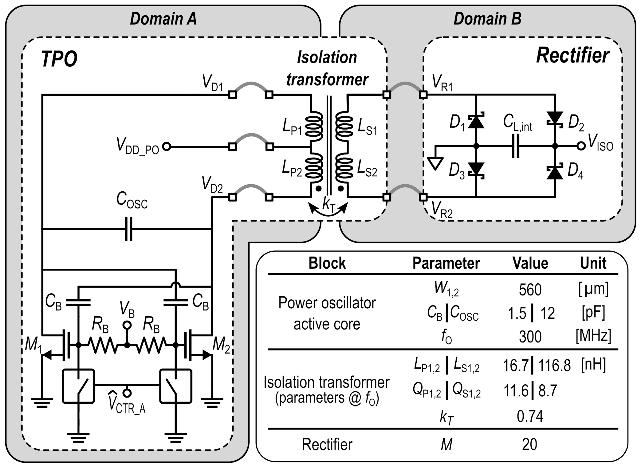
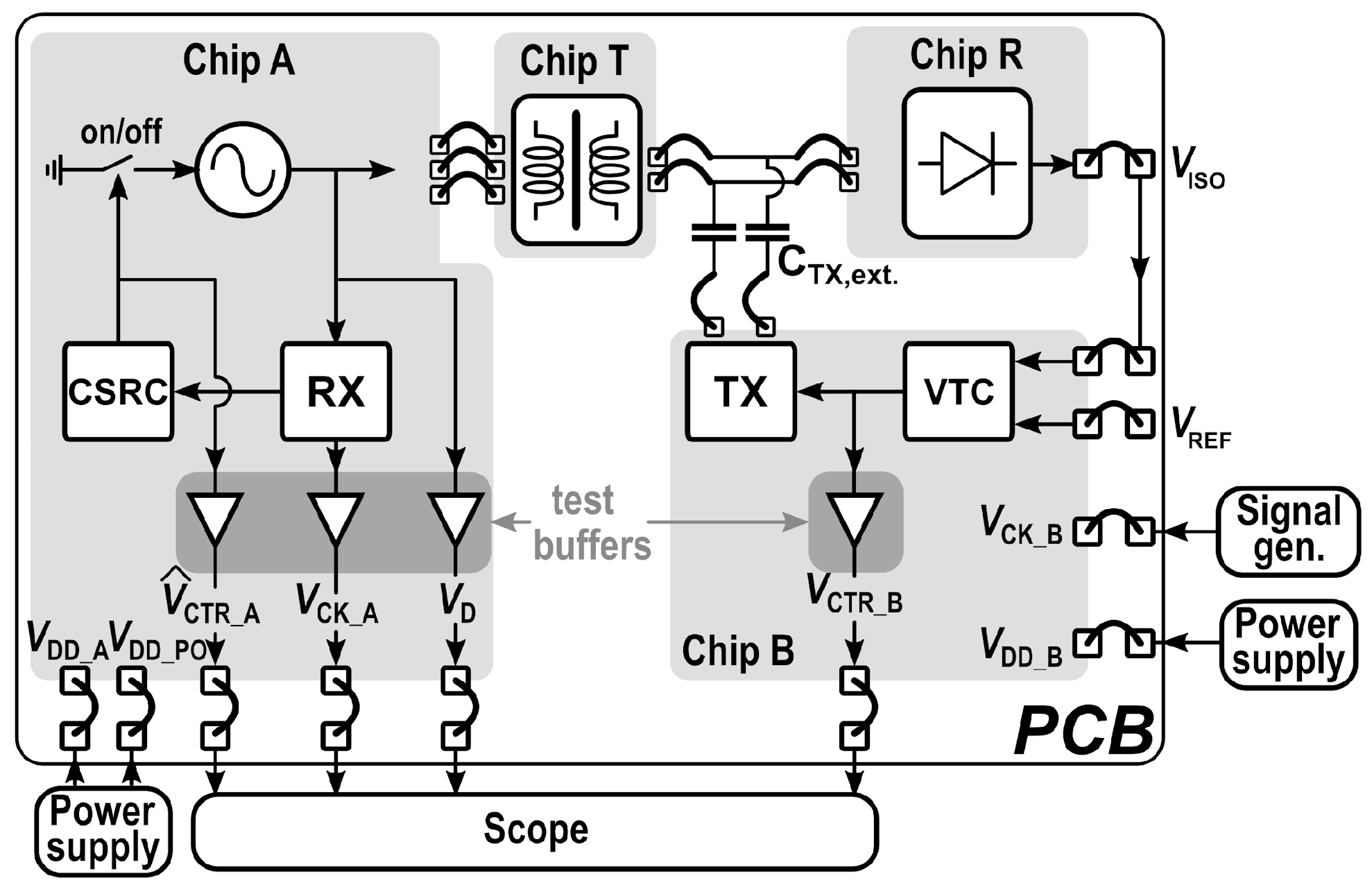
2. System Description
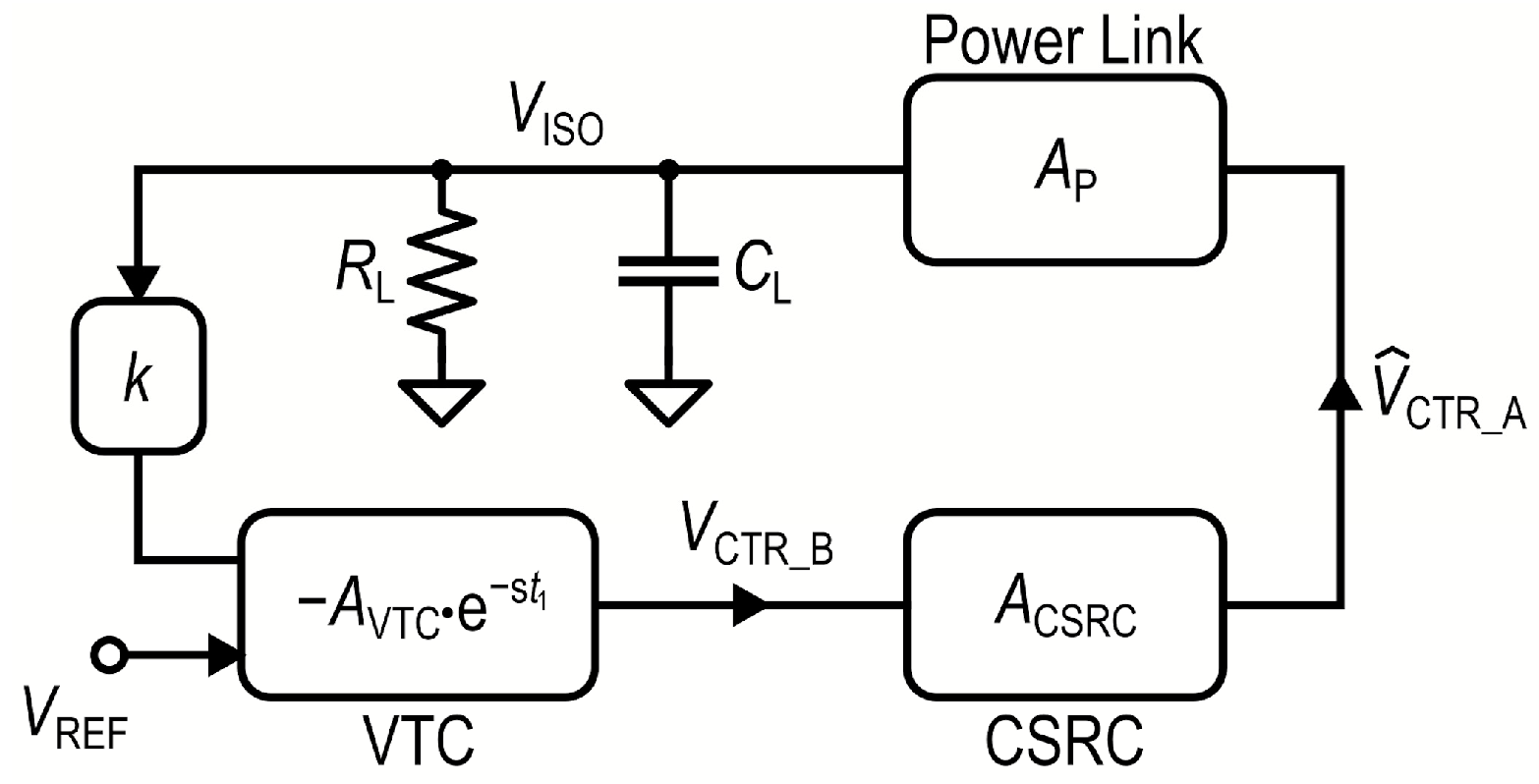
The block diagram of the proposed galvanically isolated dc–dc converter is sketched in Figure 1. It is based on a novel architecture patented by the authors with a single isolation link that is simultaneously used for power transfer and output voltage/power regulation. Specifically, the converter is composed of a transformer-based power oscillator (TPO) and a rectifier (Rect), which carry out power transfer across the galvanic isolation barrier from domain A to domain B. On the other hand, the transmission of the control signal in the opposite direction (i.e., from domain B to domain A) is achieved by means of a voltage-to-time converter (VTC) and a transmitter (TX) that performs an ASK modulation on the power signal into domain B, according to the feedback control signal. Conversely, a receiver (RX) along with a control signal reconstruction circuit (CSRC) are implemented into domain A to recover the control signal and properly drive the TPO.
The operating principle of the proposed dc–dc converter is disruptive with respect to traditional control methods despite its simplicity. Looking at the simplified block diagram in Figure 1, the dc output power, PL, is delivered to the external load, RL-CL, thanks to the rectifier. The dc output power is regulated by means of a feedback control loop, which adopts the PWM control scheme, traditionally exploited to maximize power efficiency regardless the power level to be set (i.e., the TPO operates at its maximum drain voltage). Given that a PWM scheme is used, the key point is to guarantee the proper operation of the power regulation when the power signal is off, and no control data can be transmitted. To this aim, the dc output voltage, VISO, that determines the power on the load resistance, RL, is attenuated by a proper factor, k, and compared with a reference voltage, VREF, thus producing an error signal, Vε. The VTC converts Vε after amplification into a PWM control signal, VCTR_B, whose positive time slot, τ, is proportional to Vε and then strictly related to PL. An external reference clock, VCK_B, is used to set the frequency of the control signal (i.e., fCTR_B = fCK_B/N) while acting on TX to perform the ASK modulation and hence transmit the bitstream related to VCTR_B across the isolation transformer. Into domain A, the RX recovers both the data, VCTR_A, and clock, VCK_A, signals, which drive the CSRC, turning on and off the power oscillator. The core of the CSRC is a PLL, which performs a sample and hold operation on the recovered clock frequency, fCK_A, thus continuously providing the reference clock in domain A even when the power oscillator is turned off and no data transmission occurs (i.e., VCTR_A and VCK_A are not available). Specifically, during the on phase of the power oscillator, the PLL operates in the closed-loop condition, performing at its output a square wave signal, V ^ CK_A, whose frequency is equal to fCK_A. When the power oscillator is turned off, the PLL switches to the open-loop condition, thus holding fCK_A regardless VCK_A. Accordingly, the locked signal V ^ CK_A is at first the frequency divided by a factor of N and then exploited as reference clock, VCK_FF, of a positive edge-triggered D flip-flop, D1, which provides the control signal, V ^ CTR_A, to the TPO. Specifically, the D-flip flop is set to VDD_A at the positive edge of VCK_FF and is reset to GNDA at the falling edge of VCTR_A. Therefore, the resulting square wave voltage at the D-flip flop output, V ^ CTR_A, is a replica of the original control signal, VCTR_B, thus performing a PWM control of the power oscillator.
The proposed architecture implements for the first time both power transfer and isolated power regulation using the same physical channel. For this purpose, it exploits both ASK modulation on the oscillation power signal to transmit the PWM power control signal from domain B to domain A and a PLL to perform clock recovery in domain A.

3. System Design

The dc–dc converter was designed to deliver an isolated output power of about 100 mW with a 18/20 V output voltage, by exploiting a 5 V power supply, VDD_PO, thus addressing typical gate driver applications. The voltage step-up is achieved by exploiting the turn ratio of the isolation transformer, while output power regulation is implemented thanks to a digital data transmission of the control signal that is performed by means of ASK modulation of the power oscillation, as mentioned before. Power and control signals are transferred from domain A to domain B and vice versa, respectively, using the same isolation link, thus getting rid of an additional isolation channel and reducing system size and cost. In the following, both the power and control functional links are individually detailed by using the related schematics.

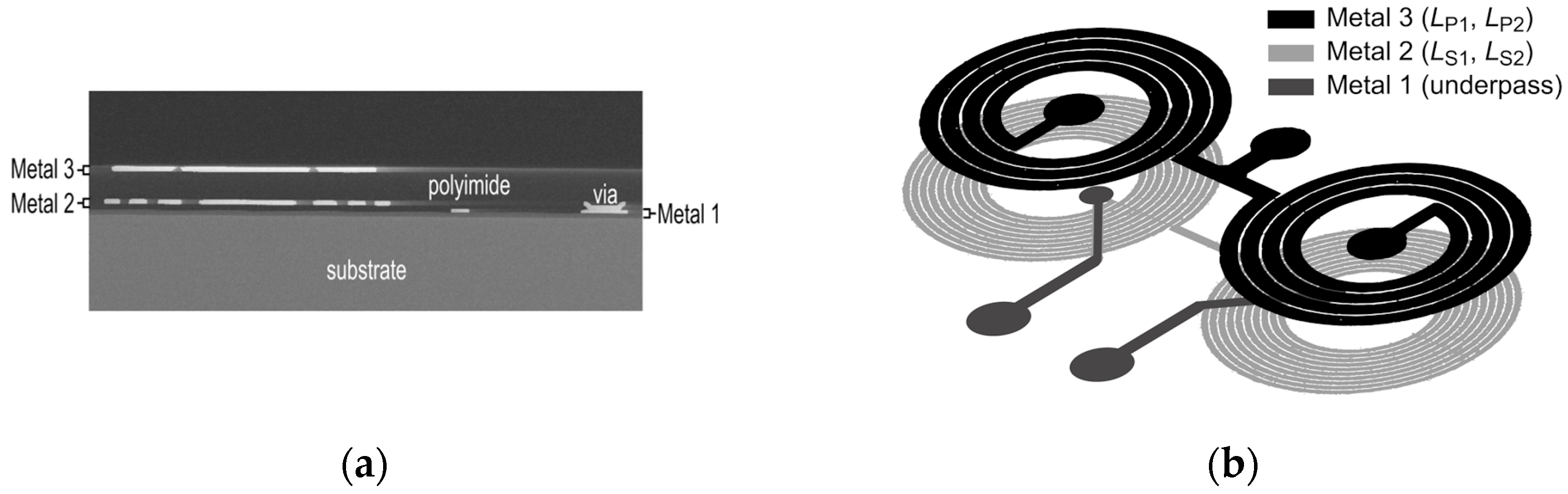
3.1. Power Link and Isolation Transformer
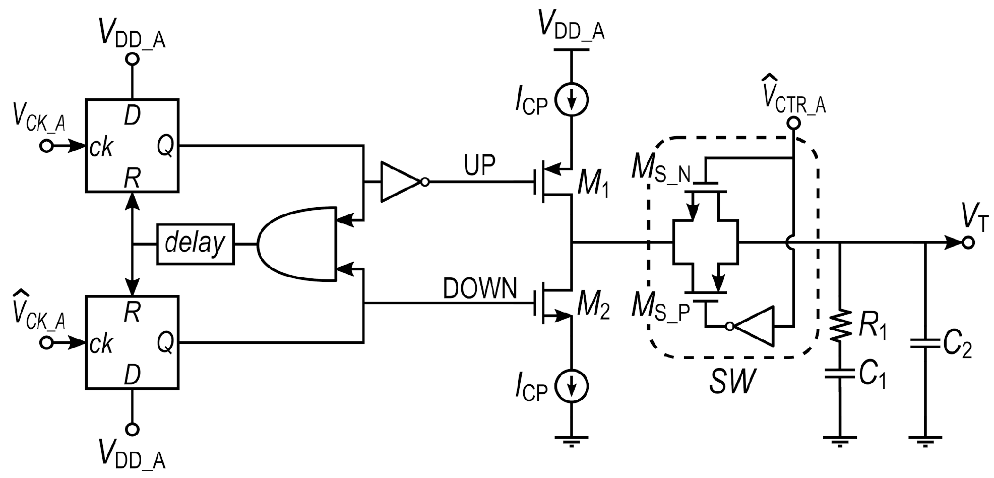
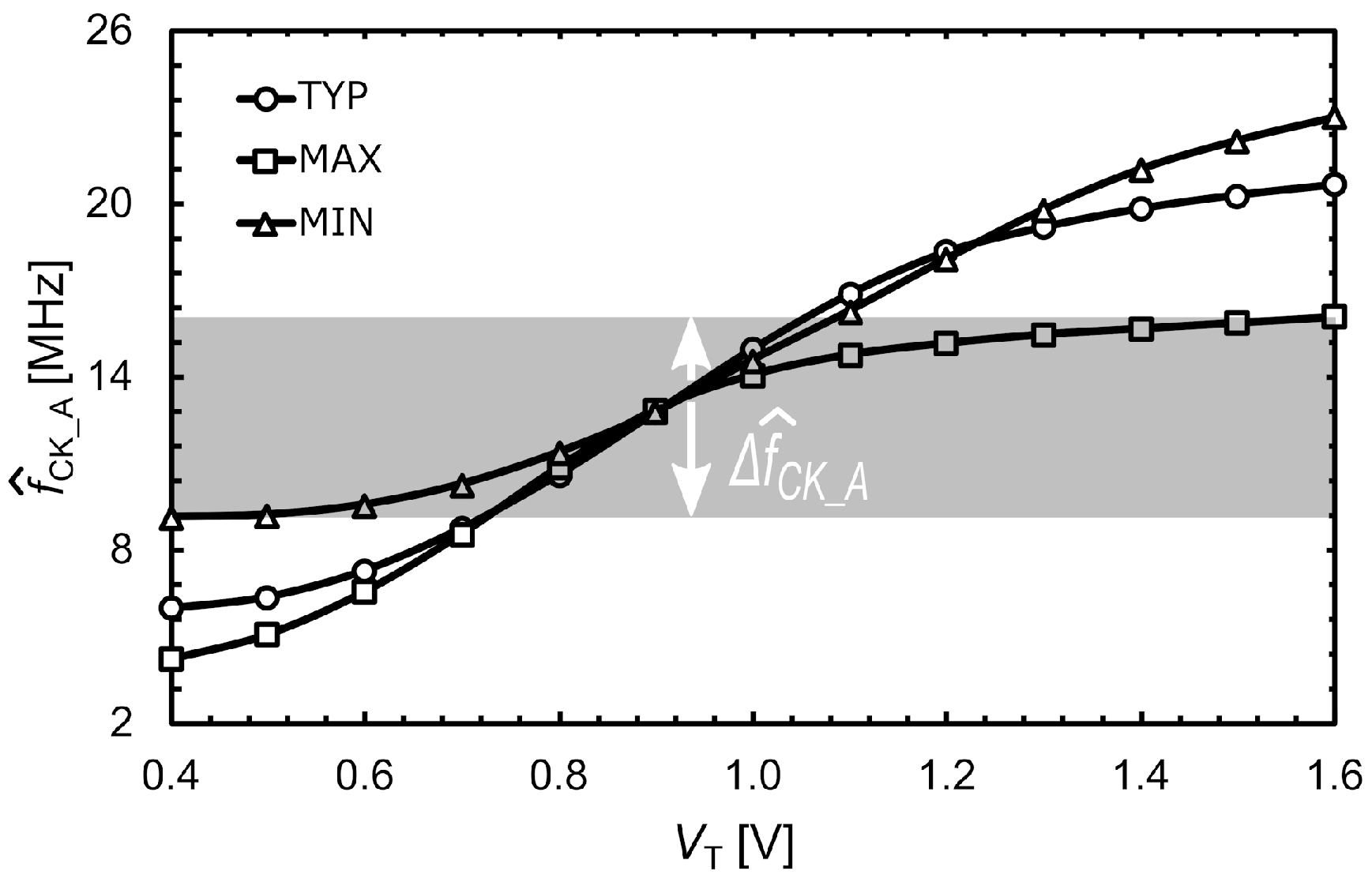
The power link is a key function for system operation since it performs power transfer through the galvanic isolation barrier and determines the power conversion efficiency (PCE) of the overall system. A simplified schematic of the power link is shown in Figure 2.
It is basically composed of a transformer-based power oscillator and a full-bridge rectifier, which perform efficient dc–ac and ac–dc conversion, respectively. The power oscillator was fabricated in 0.18 µm BCD technology, which provides high-voltage laterally diffused metal oxide semiconductor (LDMOS) transistors for high power and high frequency operation. Specifically, the power oscillator is operated in class D at 300 MHz to improve power efficiency [28,29] and consists of cross-coupled LDMOS transistors, M1,2, the LC-resonant tank made up of poly-poly capacitor, COSC, and an isolation transformer. Furthermore, the gate terminals of M1,2 are connected to on–off switches, which are driven by the PWM control signal, V ^ CTR_A, thus allowing output power regulation to be achieved by properly turning on and off the power oscillator.
The isolation transformer was implemented in a post-processed polyimide technology [25]. It takes advantage of an Au metal back-end in order to lower transformer winding resistance while reducing losses due to substrate currents (i.e., magnetically induced and vertical displacement currents) thanks to a high-resistivity substrate. Moreover, the thickness of the polyimide layer is as high as 30 μm to guarantee reinforced isolation [7,25,30]. The scanning electron microscope (SEM) cross-section of the polyimide-based transformer is depicted in Figure 3a and its geometrical structure is shown in Figure 3b.
The transformer has a differential stacked configuration that maximizes the coupling factor, kT, between primary and secondary coils, which is essential to avoid PCE degradation. A high transformer turn ratio was used to step-up the output voltage and, therefore, the geometrical parameters were chosen with the aim of maximizing the overlap between primary and secondary windings. Table 1 presents the geometrical parameters of half of the transformer coils.
Finally, center-tap connections were made available only for primary winding to allow power supply connections of the power oscillator in domain A, while the center-tap bonding wire for the secondary coil was avoided by exploiting a full-wave bridge topology for the rectifier, which allows ground connection in case of undesired electrical discharges. The rectifier chip was fabricated in a 0.13 μm standard CMOS process, providing high-voltage Schottky diodes with sub-GHz operation capability.
The power link was optimized by means of an iterative co-design between the oscillator core and the transformer, which was properly modeled with a lumped scheme [31]. For the sake of completeness, Figure 2 also contains an inset table with the design parameters of the power link.

3.2. Control Link

A simplified schematic of the control link with the main building blocks is reported in Figure 4.
The resistive divider, R1-R2, is used to obtain a proper fraction of the isolated voltage, VISO, which is compared with the reference voltage, VREF, thus driving an operational transconductance amplifier (OTA) with the error signal, . A voltage ramp is then produced by injecting the amplifier output current, IOTA, into the integration capacitor, CI. This voltage ramp drives a comparator (COMP) that resets a D flip-flop. The duration of the positive time slot, τ, of control signal VCTR_B and hence the on phase of the power oscillator is set by the slope of the voltage ramp. An external clock, VCK_B, drives a divider that imposes the frequency of VCTR_B at fCK_B/N. Time slot τ is here intended as the VTC output signal. It is given by Equation (1):
τ = V C O M P · C I G m · V ε
where VCOMP is the comparator reference voltage and Gm is the OTA transconductance. As already explained, the TX transmits the control signal across the isolation barrier. To this aim, TX performs PWM coding of VCTR_B by means of an encoder, ENC. The obtained bitstream is then transmitted by exploiting impedance mismatch at the isolation transformer secondary winding through capacitors, CTX1,2, and MOS switches, MTX1,2.
The RX block consists of a demodulator, DEM, and decoder, DEC. After the galvanic barrier, it recovers both the data (i.e., VCTR_A) and sampling clock (i.e., VCK_A). The demodulator, which is detailed in Figure 4, is made up of an envelope detector, a Sallen–Key (SK) low-pass filter, an average voltage detector, and a hysteresis comparator. A common drain pair, M3,4, with the capacitor, C1, is adopted as envelope detector. It produces the envelope signal, VENV. Then, an SK filter (i.e., R1, R2, C2, C3, and Q1,2) reduces the high frequency harmonics due to the power oscillator, while preserving the envelope signal. A further low pass filter (R3 and C4) extracts the average signal, VAV, from the SK output voltage, VSK, which is used by the comparator to produce a rail-to-rail signal, VBS (i.e., the bitstream), for the decoder.
The latter delivers both VCTR_A and VCK_A at the input of the CSRC block.
As far as the CSRC is concerned, a PLL is exploited to lock fCK_A and hold it during the power oscillator off state (i.e., when data transmission is not available). The PLL embeds a switch, SW, placed at the input of the low-pass filter (LPF) to open the PLL loop simultaneously with the power oscillator turning off. To this aim, SW is driven by V ^ CTR_A and freezes the VCO tuning voltage, VT, into the LPF capacitors when V ^ CTR_A goes low, thus maintaining the VCO output frequency f ^ CK_A to the value of fCK_A. By properly dividing f ^ CK_A thanks to a digital counter, the frequency of the reference clock, VCK_FF, is set equal to fCK_A/N, which is the same frequency as the control signal produced in domain B (i.e., fCK_B/N). VCK_FF is the input clock of the D flip-flop, D1, which provides the control signal to the TPO. Specifically, the rising edge of VCK_FF sets high V ^ CTR_A and determines the oscillator turn-on instant, whereas the falling edge of VCTR_A resets D1, imposing the duty cycle of V ^ CTR_A and hence the turn-on time of the TPO.
The PLL is the key building block of CSRC since it continuously provides an accurate reference clock (i.e., V ^ CK_A), which is exploited for the reconstruction of the control signal. Figure 5 shows a simplified schematic of the PLL forward path from the PFD/CP to the LPF made up of resistor R1 and capacitors C1 and C2.
The UP and DOWN outputs of the PFD drive the MOS transistors M1 and M2, which implement the switches that enable the CP current generators (i.e., ICP) to properly charge/discharge the second-order loop filter.
The switch placed between the PFD/CP and the filter is implemented by means of a transmission gate, SW, which exploits a complementary topology to preserve the CP output swing and minimize the charge injected into the loop filter capacitors. As far as the VCO is concerned, a ring oscillator topology is preferred, as depicted in Figure 6.
Specifically, the VCO consists of three current-controlled CMOS inverters along with CVCO capacitors. Each stage provides a delay related to the voltage swing, VS, and the slew rate IVCO/CVCO, where IVCO is the bias current of the VCO. Considering the three inverting stages, the oscillation frequency is expressed as follows:
f ^ C K _ A = I V C O 6 · V S · C V C O
The oscillation frequency is tuned by IVCO, which in turn is varied by the MOS transistor, MR. Specifically, MR mainly operates in triode region performing a variable resistance, RM, that is controlled by the loop filter output voltage, VT. Current IVCO is given in first approximation by:
I V C O = V D D _ A V S G 5 R 1 + R 2 / / R M
The simulated tuning range of the VCO for typical, minimum, and maximum corners is shown in Figure 7.
The VCO control voltage ranges from 0.4 V to 1.6 V, which are the threshold voltage of MR and the maximum allowable output voltage of CP, respectively. As is apparent, the VCO provides an oscillation frequency ranging from 3.8 MHz to 21 MHz at the nominal condition. The grey region in Figure 7 highlights the variation in f ^ CK_A due to process tolerance. It can be noticed that a range from 9.5 MHz (i.e., minimum corner) to 16.1 MHz (i.e., maximum corner) is guaranteed in the worst case. Therefore, despite the reduction in the frequency control range compared to the nominal condition, the VCO guarantees an oscillation frequency of 12.8 MHz, which is the locked frequency for the PLL. As far as the loop filter is concerned, it was sized to provide a 0.65 MHz PLL bandwidth while guaranteeing a phase margin of around 60°. Table 2 summarizes the main design parameters of the PLL.
Finally, an analysis of the stability of the control loop was carried out. To this aim, the simplified model shown in Figure 8 was used along with a single pole approximation for each block.
The open loop gain, TO, can be written as follows:
T O = k · A V T C · A C S R C · A P
where k is the resistive partition at the converter output; AVTC is the gain factor of the voltage-to-time converter; and ACSRC and AP are the gain factors of CSRC and power link, respectively. The loop gain transfer function, T(s), was evaluated by considering the main low-frequency contributions. Specifically, they are the pole of the power link at the output (i.e., RL-CL) and the delay due to VTC (about equal to the period of the PWM control signal, i.e., t1 = NTCK). It is worth noting that the delay due to the PLL was neglected since the PLL locking time was much lower than the delays introduced by other blocks.
T ( s ) = T O e t 1 s ( 1 + s R L C L )
In the worst case, a maximum 40 dB open loop gain, TO, was set. Therefore, a dominant pole compensation was implemented by sizing the load capacitance, CL, according to Equation (6):
C L = T O t 1 R L ( π 2 P M )
where PM is the phase margin expressed in radians. A capacitor, CL, of a few microfarads is sufficient to assure system stability with a 50 kHz PWM control signal.

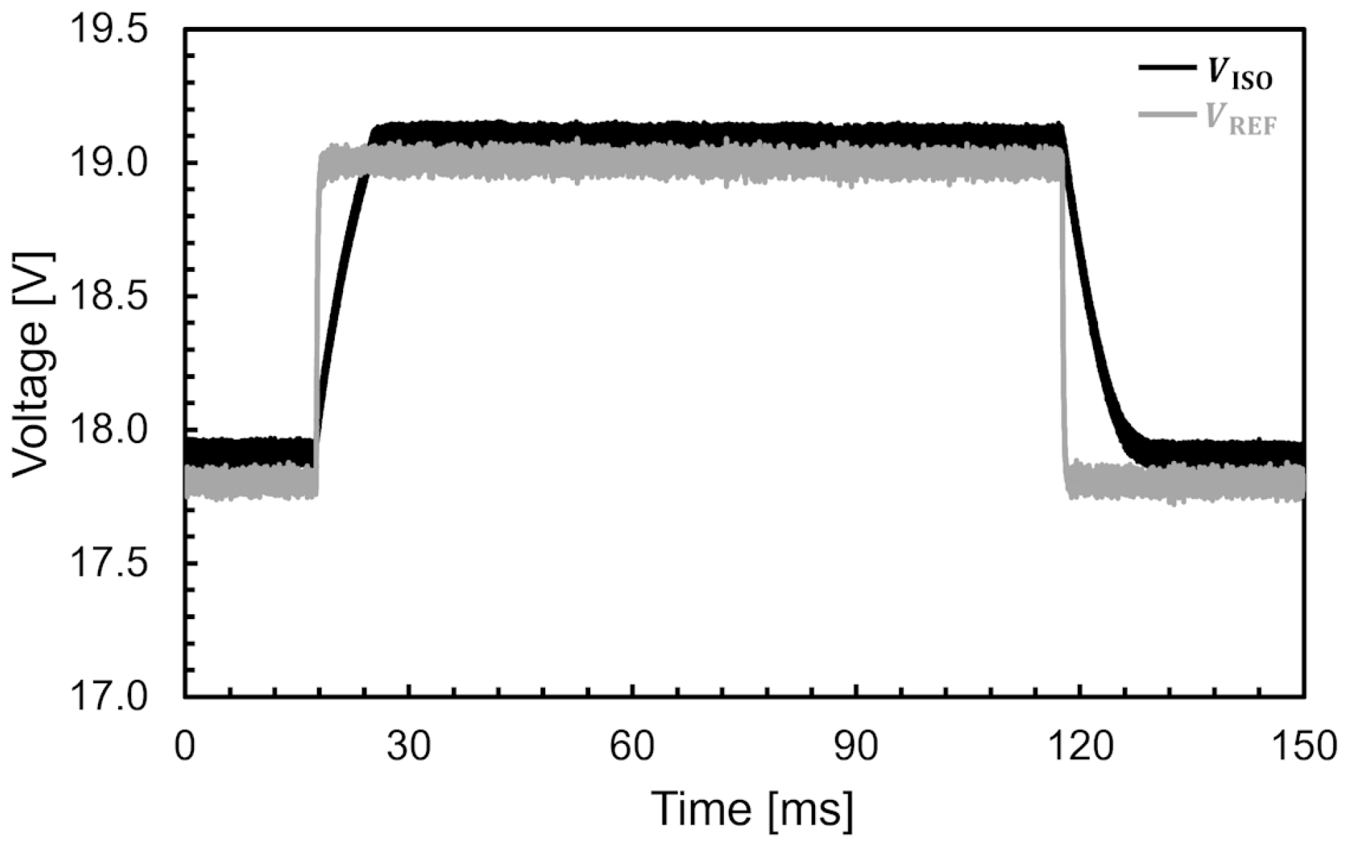
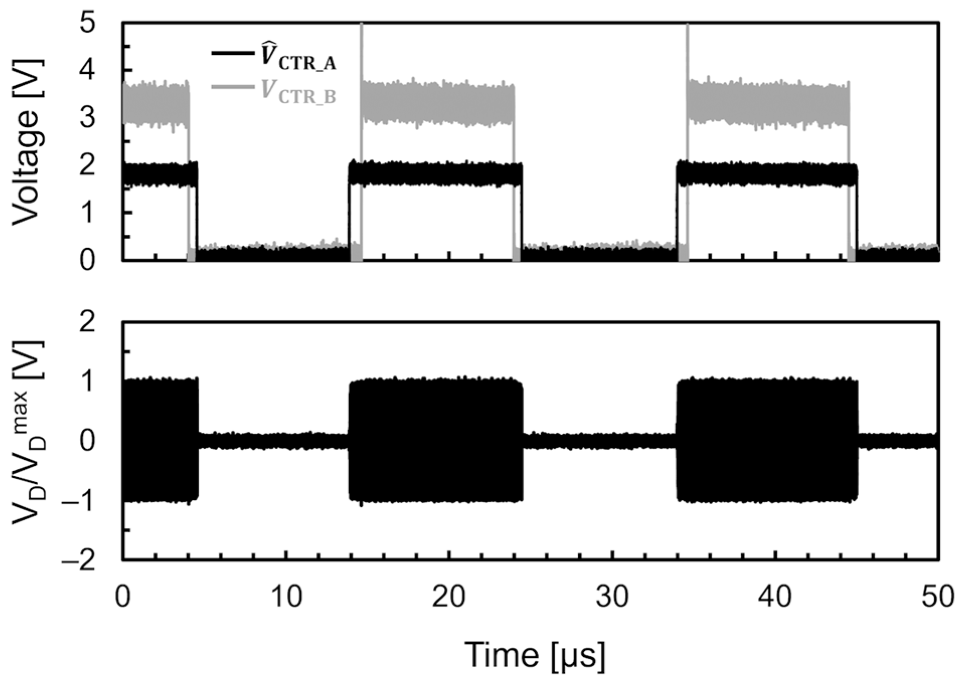
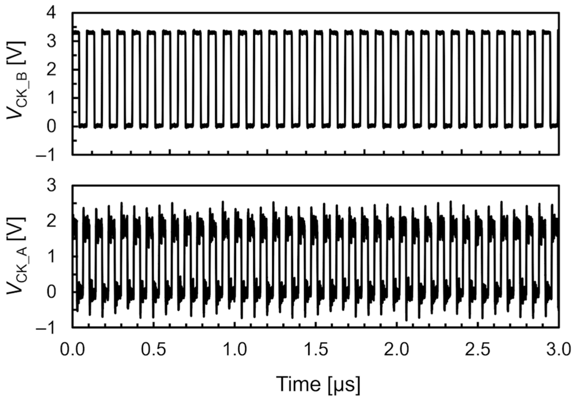
4. Experimental Results

A micrograph photo of the single-channel dc–dc converter with galvanic isolation is depicted in Figure 9, along with the die size of each chip.
The system was assembled on a customized FR4 printed circuit board (PCB) for full electrical characterization. The proposed architecture is suitable for a highly integrated implementation, either in a two-chip [23] or in a three-chip [25] SiP, depending on the adopted transformer isolation technology [32]. Since the system was designed for a reinforced isolation application, a three-chip implementation was adopted with a separated chip for the polyimide transformer. However, a four-chip solution was used for the experimental demonstration. Specifically, chip A was fabricated in a 0.18 μm BCD technology and housed the low-voltage side circuits (i.e., power oscillator, receiver, and control signal reconstruction circuit), whereas a standalone post-processed isolation transformer (i.e., chip T) was exploited to provide reinforced galvanic isolation. As far as the high-voltage side is concerned, the power rectifier was fabricated in a 0.13 μm CMOS process (i.e., chip R), since it provided high-voltage Schottky diodes. The voltage-to-time converter along with the transmitter in chip B were implemented by using the same 0.18 μm BCD technology for chip A. Moreover, dedicated pads on the PCB were designed to mount the capacitors, CTX,ext, thus externally setting the modulation index for control data transmission.
Figure 10 shows the simplified block diagram of the adopted measurement setup, which includes a digital oscilloscope for transient measurements and a signal generator to generate the reference clock signal.
Measurements were carried out at 5 V power supply, VDD_PO. An auxiliary 1.8 V power supply, VDD_A, was used for the RX and the power control circuits in chip A. On the other hand, the circuitry in chip B (i.e., the TX and VTC) was supplied by an auxiliary 3.3 V supply voltage, VDD_B, which would be provided in a final implementation by a voltage regulator scaling down the isolated output voltage, VISO. The latter was set to 19 V by the integrated power control loop. An external 12.8 MHz clock frequency (i.e., VCK_B) was used as reference to transmit the control bits and generate the internal 50 kHz PWM signal. To this aim, a division factor, N, of 256 was used for both DB and DA.
At maximum duty cycle, the system delivered up to 110 mW output power on a load resistance of 3.5 kΩ with a power conversion efficiency of about 17%. It is worth noting that the PCE was mainly affected by the four-chip assembling, which introduced additional losses in the power signal path compared to the three-chip solution. Indeed, the same isolation technology in a three-chip implementation provided a PCE as high as 25%, as reported in [32].
Figure 11 shows the transient response of the isolated voltage, VISO, to a step from 17.8 V to 19 V of the reference voltage, VREF, which corresponds to a variation of the output power, PISO, from about 90 mW to 100 mW on a 3.5 kΩ load resistance. The output capacitance, CL, is fixed to 3.9 μF, which guarantees the stability of the control loop while providing a reduced output ripple. As is apparent, the isolated output voltage is well regulated by the control loop to the external reference voltage, thus demonstrating the effectiveness of the proposed power control technique.
For the sake of completeness, the PWM control signals generated in Chip B and reconstructed in Chip A are also shown in Figure 12, along with the normalized voltage waveform at the drain terminal of the power oscillator. The RF power signal is turned on and off according to the desired output power. Specifically, the control loop imposes the duty cycle of the PWM signal at about 55% to set the steady-state output power to around 60 mW.
Figure 13 and Figure 14 show the normalized RF power oscillation at the rising and falling edges of the PWM control signal, respectively. A modulation index around 10% was chosen to preserve power conversion efficiency.
Figure 15 depicts the input, VCK_B, and RX output, VCK_A, clock signals at domain B and domain A, respectively, within the on phase of the power oscillator. It is worth noting that although VCK_A is not available during the power oscillator off phase, the control signal in domain A is properly reconstructed thanks to the PLL.
Finally, the dc–dc converter performance is summarized in Table 3 and compared with recent state-of-the-art converters providing similar power levels.

5. Conclusions

A galvanically isolated dc–dc converter has been presented, which features a novel system architecture for power control functionality. Indeed, traditional isolated dc–dc converters exploit the PWM control scheme with a dedicated isolation link to perform efficient power regulation. Differently from the common approach, the proposed architecture implements a feedback control loop on the same physical isolation link used for power transfer, thus overcoming the need for an additional isolation channel with the consequent reduction in size, power consumption, and cost. To the authors’ knowledge, this is the very first integrated system that performs power transfer and closed-loop PWM output voltage/power regulation in the same isolation link.

6. Patents

A. Parisi, N. Greco, N. Spina, E. Ragonese, and G. Palmisano. Galvanic isolation circuit and system and a corresponding method of operation. U.S. Patent. US10917091B2, granted 9 February 2021.

Author Contributions

Conceptualization, A.P. and G.P.; validation, A.P. and A.C.; formal analysis, A.P. and E.R.; investigation, A.P., E.R. and N.S.; project administration, G.P.; supervision, G.P. and E.R.; writing—original draft preparation, A.P. and E.R.; writing—review and editing, E.R. and G.P. All authors have read and agreed to the published version of the manuscript.

Funding

This research received no external funding.

Data Availability Statement

The data presented in this study are available on request from the corresponding author.

Conflicts of Interest

Authors Alessandro Parisi, Nunzio Spina and Alessandro Castorina were employed by the company STMicroelectronics. The remaining authors declare that the research was conducted in the absence of any commercial or financial relationships that could be construed as a potential conflict of interest.

References

  1. Analog Devices. Surging Across the Barrier: Digital Isolators Set the Standard for Reinforced Insulation. Available online: https://www.analog.com/en/resources/technical-articles/digital-isolators-set-the-standard-for-reinforced-insulation.html (accessed on 27 March 2025).
  2. NVE Corporation. Isolator High Voltage Safety Standards. 2024. Available online: https://www.nve.com (accessed on 28 March 2025).
  3. Maniar, K.; Mappus, S.; Merkin, T.; Triano, A.; Trowbridge, L. Addressing High-Voltage Design Challenges with Reliable and Affordable Isolation Technologies. Available online: https://www.ti.com/lit/wp/slyy204c/slyy204c.pdf (accessed on 28 March 2025).
  4. Krone, A.; Tuttle, T.; Scott, J.; Hein, J.; Dupuis, T.; Sooch, N. A CMOS direct access arrangement using digital capacitive isolation. In Proceedings of the IEEE International Solid-State Circuits Conference, San Francisco, CA, USA, 7 February 2001; pp. 300–301. [Google Scholar]
  5. Kaeriyama, S.; Uchida, S.; Furumiya, M.; Okada, M.; Maeda, T.; Mizuno, M. A 2.5 kV isolation 35 kV/us CMR 250 Mbps digital isolator in standard CMOS with a small transformer driving technique. IEEE J. Solid-State Circuits 2012, 47, 435–443. [Google Scholar]
  6. Ma, S.; Feng, J.; Zhao, T.; Chen, B. A fully isolated amplifier based on charge-balanced SAR converters. IEEE Trans. Circuits Syst. I Reg. Papers 2018, 65, 1795–1804. [Google Scholar]
  7. DIN VDE Semiconductor Devices-Magnetic and Capacitive Coupler for Basic and Reinforced Isolation, VDE Verlag VDE V 0884–11, January 2017. Available online: https://www.vde-verlag.de/standards/0800375/din-vde-v-0884-11-vde-v-0884-11-2017-01.h (accessed on 28 March 2025).
  8. Chen, B. iCoupler Products with isoPower Technology: Signal and Power Transfer Across Isolation Barrier Using Microtransformers. Analog Devices, Norwood, MA, USA, Tech. Rep. Available online: https://www.analog.com/en/resources/technical-articles/icoupler-products-with-isopower-technology.html (accessed on 28 March 2025).
  9. Chen, B. Fully integrated isolated DC-DC converter using micro transformers. In Proceedings of the IEEE Applied Power Electronics Conference and Exposition (APEC), Austin, TX, USA, 24–28 February 2008; pp. 335–338. [Google Scholar]
  10. Qin, W.; Yang, X.; Ma, S.; Liu, F.; Zhao, Y.; Zhao, T.; Chen, B. An 800 mW fully integrated galvanic isolated power transfer system meeting CISPR 22 Class-B emission levels with 6 dB margin. In Proceedings of the IEEE International Solid-State Circuits Conference, San Francisco, CA, USA, 17–21 February 2019; pp. 246–248. [Google Scholar]
  11. Tianting, Z.; Yue, Z.; Baoxing, C. An isolated DC-DC converter with fully integrated magnetic core transformer. In Proceedings of the IEEE Custom Integrated Circuits Conference (CICC), Austin, TX, USA, 30 April–3 May 2017; pp. 1–4. [Google Scholar]
  12. Chen, B. Isolated half-bridge gate driver with integrated high-side supply. In Proceedings of the IEEE Power Electronics Specialists Conference (PESC), 15–19 June 2008; pp. 3615–3618. [Google Scholar]
  13. Kamath, A.S.; Soundarapandian, K. High-Voltage Reinforced Isolation: Definitions and Test Methodologies. Texas Instrum., Dallas, TX, USA, Tech. Rep. November 2014. Available online: https://www.ti.com/lit/wp/slyy063/slyy063.pdf?ts=1741590137990 (accessed on 28 March 2025).
  14. Chen, B. High Frequency Power Converter Based on Transformers. U.S. Patent 7983059B2, 19 July 2011. [Google Scholar]
  15. Palumbo, V.; Ghidini, G.; Carollo, E.; Toia, F. INTEGRATED Transformer. U.S. Patent 10236115B2, 19 March 2019. [Google Scholar]
  16. Moghe, Y.; Terry, A.; Luzon, D. Monolithic 2.5 kV RMS, 1.8 V–3.3 V dual-channel 640Mbps digital isolator in 0.5 μm SOS. In Proceedings of the IEEE International SOI Conference, Napa, CA, USA, 1–4 October 2012; pp. 1–2. [Google Scholar]
  17. Pan, D.; Xiong, Z.; Lu, Q.; Miao, F.; Wu, L.; Cheng, L. A 250-Mb/s on-chip capacitive digital isolator with adaptive frequency control. IEEE Solid-State Circuits Lett. 2024, 7, 231–234. [Google Scholar]
  18. Texas Instruments. ISO7841x High-Performance, 8000-VPK Reinforced Quad-Channel Digital Isolator. Available online: http://www.ti.com (accessed on 28 March 2025).
  19. TI. Isolated Gate Drivers. Available online: https://www.ti.com/power-management/gate-drivers/isolated-gate-drivers/overview.html (accessed on 29 August 2021).
  20. Mahalingam, P.; Guiling, D.; Lee, S. Manufacturing challenges and method of fabrication of on-chip capacitive digital isolators. In Proceedings of the International Symposium on Semiconductor Manufacturing, Santa Clara, CA, USA, 15–17 October 2007; pp. 1–4. [Google Scholar]
  21. Analog Devices. ADuM6200-Dual-Channel, 5 kV Isolators with Integrated DC-to-DC Converter Datasheet. 2020. Available online: http://www.analog.com (accessed on 28 March 2025).
  22. Tan, Z.; Mueck, M.; Du, X.H.; Getzin, L.; Guidry, M.; Keating, S.; Xing, X.; Chen, B. A fully isolated delta-sigma ADC for shunt based current sensing. IEEE J. Solid-State Circuits 2016, 51, 2232–2240. [Google Scholar] [CrossRef]
  23. Ragonese, E.; Spina, N.; Castorina, A.; Lombardo, P.; Greco, N.; Parisi, A.; Palmisano, G. A fully integrated galvanically isolated DC-DC converter with data communication. IEEE Trans. Circuits Syst. I Reg. Papers 2018, 65, 1432–1441. [Google Scholar]
  24. Lombardo, P.; Fiore, V.; Ragonese, E.; Palmisano, G. A fully integrated half-duplex data/power transfer system with up to 40 Mb/s data rate, 23mW output power and on-chip 5 kV galvanic isolation. In Proceedings of the IEEE International Solid-State Circuits Conference (ISSCC), San Francisco, CA, USA, 31 January–4 February 2016; pp. 300–301. [Google Scholar]
  25. Parisi, A.; Ragonese, E.; Spina, N.; Palmisano, G. Galvanically isolated DC–DC converter using a single isolation transformer for multi-channel communication. IEEE Trans. Circuits Syst. I Reg. Papers 2020, 67, 4434–4444. [Google Scholar]
  26. Hu, T.; Huang, M.; Martins, R.P.; Lu, Y. A 750 mW, 37% peak efficiency isolated DC–DC converter with 54/18Mb/s full-duplex communication using a single pair of transformers. In Proceedings of the IEEE International Solid-State Circuits Conference (ISSCC), San Francisco, CA, USA, 18–22 February 2024; pp. 504–506. [Google Scholar]
  27. Hu, T.; Lu, Y.; Martins, R.P.; Huang, M. An isolated DC–DC converter with full-duplex communication using a single pair of transformers. IEEE J. Solid-State Circuits 2024. early access. [Google Scholar] [CrossRef]
  28. Fanori, L.; Andreani, P. Class-D CMOS oscillators. IEEE J. Solid-State Circuits 2013, 48, 3105–3119. [Google Scholar] [CrossRef]
  29. Lee, H.-C.; Jang, S.-L.; Wang, Y.-C. Fully-integrated capacitive cross-coupled class-D oscillator with frequency doubler. In Proceedings of the 2020 International Workshop on Electromagnetics: Applications and Student Innovation Competition (iWEM), Makung, Taiwan, 26–28 August 2020; pp. 1–2. [Google Scholar]
  30. Yun, R.; Sun, J.; Gaalaas, E.; Chen, B. A transformer-based digital isolator with 20kVPK surge capability and >200 kV/μS common mode transient immunity. In Proceedings of the IEEE Symposium on VLSI Circuits (VLSI-Circuits), Honolulu, HI, USA, 15–17 June 2016; pp. 1–2. [Google Scholar]
  31. Greco, N.; Parisi, A.; Spina, N.; Ragonese, E.; Palmisano, G. Scalable lumped models of integrated transformers for galvanically isolated power transfer systems. Integration 2018, 63, 323–331. [Google Scholar]
  32. Ragonese, E.; Spina, N.; Parisi, A.; Palmisano, G. An experimental comparison of galvanically isolated DC-DC converters: Isolation technology and integration approach. Electronics 2021, 10, 1186. [Google Scholar] [CrossRef]
  33. Ishihara, H.; Onizuka, K. A fully-generic-process galvanic isolator for gate driver with 123 mW 23% power transfer and full-triplex 21/14/0.5 Mb/s bidirectional communication utilizing reference-free dual-modulation FSK. In Proceedings of the IEEE International Solid-State Circuits Conference, San Francisco, CA, USA, 16–20 February 2020; pp. 300–301. [Google Scholar]
  34. Li, L.; Fang, X.; Wu, R. An 11 MHz fully integrated 5 kV isolated DC-DC converter without cross-isolation-barrier feedback. In Proceedings of the IEEE International Solid-State Circuits Conference, San Francisco, CA, USA, 16–20 February 2020; pp. 292–294. [Google Scholar]
Figure 1. Architecture of the proposed galvanically isolated dc–dc converter.
Electronics 14 01368 g001
Figure 2. Simplified schematic of the power link with main design parameters.
Electronics 14 01368 g002
Figure 3. (a) SEM cross-section of the polyimide-based isolation transformer with three Au metal layers. (b) Three-dimensional view of the isolation stacked transformer. Reproduced from [25]. Copyright 2020, IEEE.
Electronics 14 01368 g003
Figure 4. Simplified schematic of the control link.
Electronics 14 01368 g004
Figure 5. Schematic of the PFD/CP along with the low-pass filter.
Electronics 14 01368 g005
Figure 6. Schematic of the VCO.
Electronics 14 01368 g006
Figure 7. Simulated VCO tuning range for typical, minimum, and maximum corners.
Electronics 14 01368 g007
Figure 8. Simplified model of the control link for stability analysis.
Electronics 14 01368 g008
Figure 9. Micrograph of the dc–dc converter.
Electronics 14 01368 g009
Figure 10. Simplified block diagram of the measurement setup.
Electronics 14 01368 g010
Figure 11. VISO transient response in closed-loop operation.
Electronics 14 01368 g011
Figure 12. PWM control signals and normalized RF power oscillation at an output power of 60 mW.
Electronics 14 01368 g012
Figure 13. Transient signals at the power oscillator switching on.
Electronics 14 01368 g013
Figure 14. Transient signals at the power oscillator switching off.
Electronics 14 01368 g014
Figure 15. Input and recovered clock signals.
Electronics 14 01368 g015
Table 1. Geometrical parameters of the isolation transformer.
ParametersPrimary CoilSecondary Coil
Number of turns (n)3.7510
Metal width (w) [µm]379.8
Metal spacing (s) [µm]9.59.5
Internal diameter (dIN) [µm]300300
Outer diameter (dOUT) [µm]676686
Table 2. Main design parameters of the PLL.
BlockParameterValueUnit
Charge pumpICP1µA
Switch, SWW/LMS_P470/180nm/nm
W/LMS_N280/180nm/nm
R1290kΩ
Loop filterC110pF
C20.5pF
Voltage-controlled
oscillator
CVCO300fF
R121.5kΩ
R277.5kΩ
W/LMR0.28/0.4µm/µm
W/LMINV,N1.4/180µm/nm
W/LMINV,P2/180µm/nm
Table 3. Summarized performance and comparison with state of the art.
Parameters[23][25][33][34]This Work
Supply voltage [V]3.35 *5.53.35 *
Isolated output voltage [V]3.33.343.320
Max. output power [mW]9350123165110
Power efficiency [%]1914233417
Oscillation frequency [MHz]350300≈10011270
Control scheme/frequency [kHz]PWM/100Continuous timen.a. **Open-loop capacitor-based controllerPWM/50
Isolation levelBasicReinforcedBasicBasicReinforced
Silicon technology0.35 μm BCD0.18 μm BCD, Schottky diode, 0.13 μm CMOS0.13 μm CMOS0.35 μm BCD0.18 μm BCD, Schottky diode,
0.13 μm CMOS,
Isolation technologyIntegrated SiO2 transformers
with Cu/Al metals
Post-processed polyimide transformer with Au metalsPCB
transformers
Coreless micro transformerPost-processed polyimide transformer with Au metals
No. of isolation
transformers
21211
* Power oscillator supply voltage; ** The output voltage is not controlled.
Disclaimer/Publisher’s Note: The statements, opinions and data contained in all publications are solely those of the individual author(s) and contributor(s) and not of MDPI and/or the editor(s). MDPI and/or the editor(s) disclaim responsibility for any injury to people or property resulting from any ideas, methods, instructions or products referred to in the content.

