Abstract
The three-level simplified neutral point clamped (3L-SNPC) inverter has received increasing attention in recent years due to its potential applications in electrical drives and smart grids with renewable energy integration. However, most existing research has primarily focused on control development, with limited studies investigating modulation strategies or analyzing inverter losses under varying operating conditions. These aspects are critical for practical industrial applications. To address this gap, this paper proposes a novel carrier-based space vector pulse width modulation (CB-SVPWM) strategy for the 3L-SNPC inverter, aimed at simplifying PWM implementation and reducing cost. The proposed modulation strategy is experimentally evaluated by comparing inverter losses and total harmonic distortion with those of the conventional three-level neutral point clamped (3L-NPC) inverter under an equivalent carrier-based modulation scheme. A comprehensive comparative analysis is conducted across the full modulation range to demonstrate the effectiveness of the proposed approach, achieving a 13.2% reduction in total power loss, a 33.6% improvement in execution time, and maintaining a comparable weighted total harmonic distortion (WTHD) with a deviation within 0.04% of the conventional 3L-NPC inverter.
1. Introduction
Three-level neutral point clamped (3L-NPC) inverters have been widely adopted in low- to medium-voltage applications, such as electric machine drives [1,2], solar photovoltaic integration [3,4], vehicle traction [5] and propulsion [6,7], and grid integration [8,9], due to their low total harmonic distortion (THD), reduced voltage stress, and high voltage handling capability. However, two major drawbacks of conventional 3L-NPC inverters are their reliance on a large number of power semiconductors and their relatively high-power losses [10,11].
To reduce the number of semiconductors and the associated losses in low-voltage applications, J.W. Kolar et al. introduced the three-level T-type inverter [12] which eliminates the need for six clamping diodes while offering improved efficiency over a broad modulation range. Further reduction in semiconductor count is achieved with the three-level simplified NPC (3L-SNPC) inverter topology [13,14]. Compared to the three-level T-type inverter, the 3L-SNPC inverter eliminates two additional active switches along with their corresponding driver circuits, leading to lower system costs. Additionally, it mitigates neutral point voltage (NPV) fluctuations by eliminating medium voltage vectors (VVs) from its space vector diagram. Given these characteristics, the 3L-SNPC inverter, especially when paired with an efficient modulation scheme, holds strong potential for industrial applications where cost, simplicity, and thermal performance are critical. These include electric vehicle motor drive systems, renewable energy inverters, and compact, low-cost industrial power converters, where reduced switching losses and simpler implementation contribute to improved system-level efficiency and cost-effectiveness.
Despite these advantages, existing research on the 3L-SNPC inverter has primarily focused on control strategies [15,16,17,18,19,20,21,22], with minimal attention given to carrier-based modulation and loss analysis. Most carrier-based space vector pulse width modulation (CB-SVPWM) techniques are designed for 3L-NPC inverters, where the symmetrical three-phase structure allows direct implementation using standard modulation frameworks. However, these conventional CB-SVPWM methods fail to account for the inherent asymmetry of the 3L-SNPC inverter, making direct application infeasible. Specifically, traditional NPC-based carrier modulation methods rely on the presence of medium VVs to synthesize the reference vector accurately. In the 3L-SNPC topology, these medium VVs are absent, which restricts the available switching sequences. Additionally, direct carrier-based SVM implementation in the 3L-SNPC inverter may cause phase voltage imbalance due to the missing voltage states, potentially leading to increased harmonic distortion and modulation instability.
Conventional modulation methods [23,24] for multilevel inverters are not directly applicable due to the absence of medium VVs. For instance, a previously proposed modulation scheme for the 3L-SNPC inverter faces challenges in maintaining NPV balance under high modulation indices [14]. Furthermore, the asymmetric three-phase structure of the 3L-SNPC inverter prevents direct implementation of commonly used carrier-based space vector modulation (SVM) techniques [25,26]. A lookup-table-based enhanced SVM method has been introduced to reduce NPV fluctuations, but it suffers from drawbacks such as variable switching frequency, high design complexity, and increased hardware costs [27]. In 2019, a two-stage model predictive control strategy was proposed to regulate 3L-SNPC inverters connecting to an interior permanent magnet synchronous machine (IPMSM) [28], which achieved a 50% reduction in common-mode voltage amplitude (from 133 V to 67 V) and maintained balanced NPV under varying power factor conditions. In the same year, a deadbeat-based model predictive control approach was developed for 3L-SNPC inverter-fed motor drives, demonstrating excellent drive performance [20] and demonstrating smooth torque response and comparable performance at one-fourth the sampling frequency (5 kHz against 20 kHz) compared to conventional PTC. However, this approach relies on a non-carrier-based SVM, necessitating an additional complex programmable logic device (CPLD) or field-programmable gate arrays (FPGAs) for implementation, with a significant price increase compared to simple logic gates. Notably, none of the aforementioned studies have analysed the loss characteristics of the 3L-SNPC inverter.
In practice, a carrier-based SVM strategy for the 3L-SNPC inverter that ensures NPV balance across the full modulation range has rarely been studied. Furthermore, a comprehensive investigation into conduction and switching losses under varying modulation indices remains necessary. These two aspects are critical for industrial applications. On one hand, carrier-based SVM enables simplified modulation implementation with minimal hardware cost. On the other hand, a detailed loss analysis across the full modulation range provides valuable reference for power electronics engineers. To address these gaps, this paper presents a novel carrier-based SVM strategy that is easy to implement while maintaining NPV balance and delivering superior current performance across the full modulation range. In addition, a comprehensive evaluation of conduction and switching losses is performed and compared with those of a conventional 3L-NPC inverter using an equivalent modulation scheme. To further illustrate the structural and operational differences between the 3L-SNPC and 3L-NPC inverters, Table 1 presents a comparative analysis of key characteristics, including hardware complexity, available voltage vectors, execution time, harmonic distortion, and power loss.

Table 1.
Comparative table for property and performance metrics between the 3L-SNPC and 3L-NPC inverter under the proposed method.
The key contributions of this paper are summarized below:
- A CB-SVPWM strategy is proposed for the 3L-SNPC inverter achieving low implementation cost and simplified real-time control. The proposed method effectively addresses the challenges of traditional carrier-based modulation in 3L-SNPC inverters by providing a computationally efficient alternative.
- The proposed modulation strategy utilizes XOR logic gates to replace FPGAs or CPLDs through hardware implementation and lowered system complexity and computational burden. This approach eliminates the need for lookup tables, making it more suitable for cost-sensitive applications.
- A comparative analysis between the 3L-SNPC and the conventional 3L-NPC topology under an equivalent modulation scheme is carried out. This study provides quantitative insights into modulation performance, efficiency, and system behavior across a full operating range.
- Loss characteristics including switching and conduction loss analysis of both inverters are presented to clearly demonstrate the advantages and disadvantages of the 3L-SNPC inverter. The findings provide a better understanding of power dissipation characteristics and their impact on overall inverter efficiency.
2. System Modeling
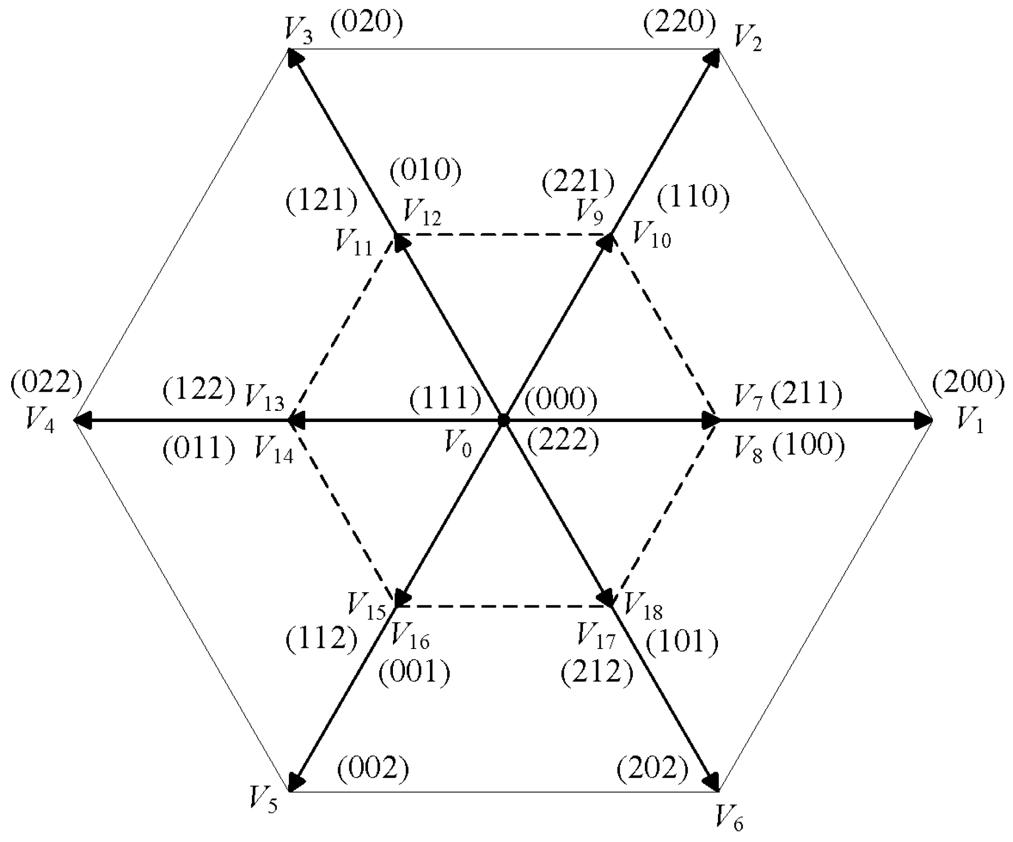
The circuit topology of the 3L-SNPC inverter is illustrated in Figure 1. It consists of a dual buck converter interfaced with a conventional two-level voltage source inverter (2L-VSI). Two capacitors of equal capacitance are connected to the neutral point of the front-end dual buck converter, ensuring voltage balance. Table 2 provides a summary of the switching logic for the dual buck converter, where , , , and represent different switching combinations. The voltages and correspond to the positive and negative terminal voltages of the dual buck converter. Based on this configuration, the space vector diagram of the 3L-SNPC inverter can be derived, as shown in Figure 2.
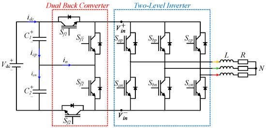
Figure 1.
Circuit topology of the 3L-SNPC inverter.
Table 2.
Switching logic of the front-end dual buck converter.
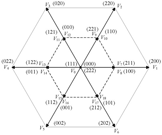
Figure 2.
Space vector diagram of the 3L-SNPC inverter.
The space vector diagram of the 3L-SNPC inverter consists of 21 voltage vectors (VVs), categorized as large, small, or zero VVs. Notably, in the 3L-SNPC inverter, six medium VVs are absent compared to the conventional 3L-NPC and T-type topologies. Each VV is represented using a three-digit notation, where ‘2’, ‘1’, and ‘0’ correspond to the three voltage levels , , and 0, respectively.
In the 3L-SNPC inverter, vector synthesis is restricted to the available 21 voltage vectors (VVs) instead of 27 VVs in the traditional 3L-NPC inverter. Among these, all large vectors consist only of ‘2’ and ‘0’, indicating a full DC voltage level. As a result, the dual buck converter maintains a consistent switching combination of ‘11’ of and for all large VVs. Importantly, large VVs do not contribute to NPV imbalance, making them advantageous for maintaining system stability.
According to the space vector diagram, generating a large VV, such as (200), requires applying the aforementioned switching combination. Consequently, the switching state of the two-level inverter (2LI) is set to ‘100’, corresponding to and . Under these conditions, the capacitor currents can be expressed as [20]
where and represent the currents flowing through capacitors and , respectively. Moreover, the neutral point current can be modeled as follows [25]:
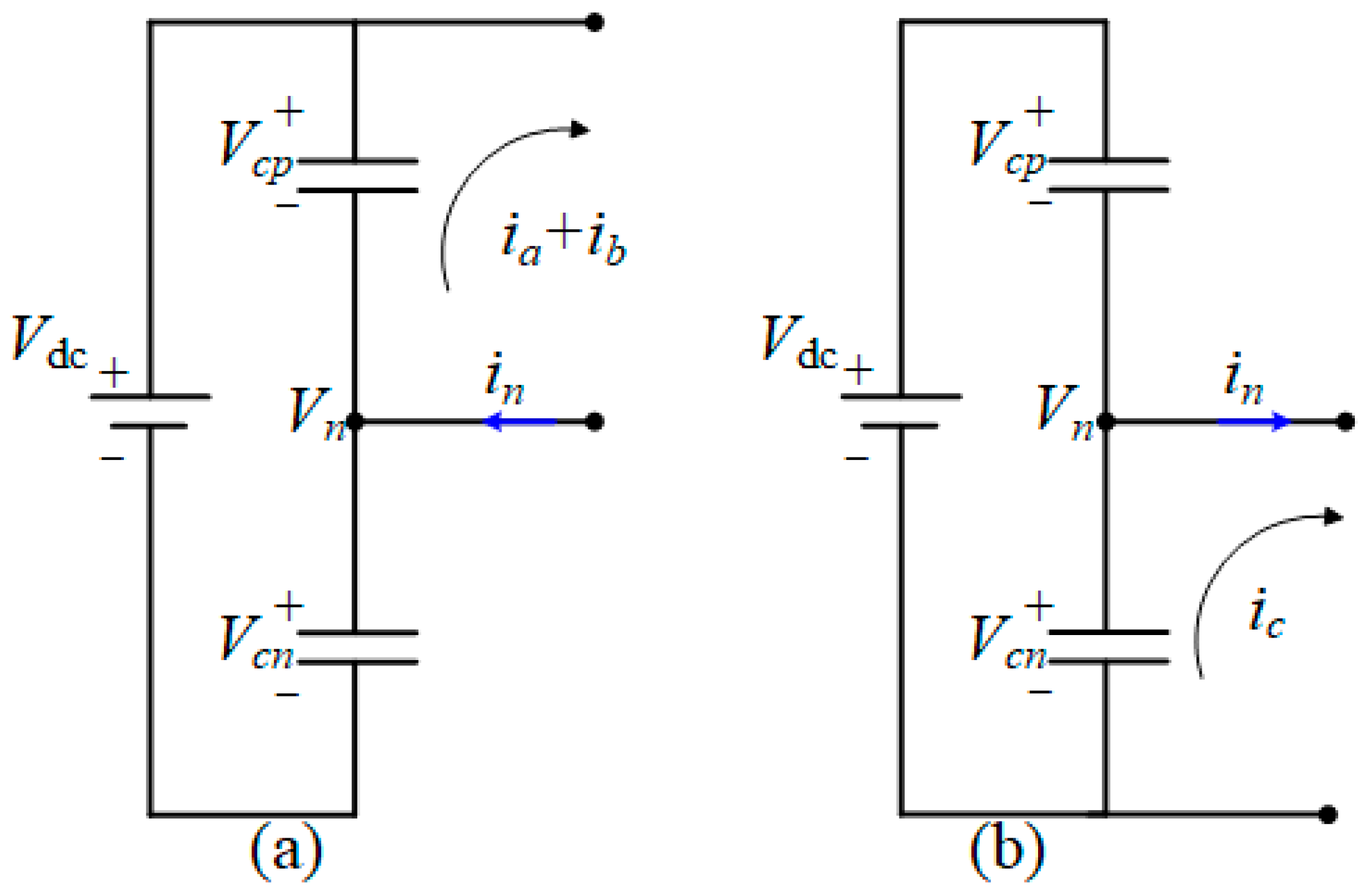
where , and represent the currents generated by each phase leg, while corresponds to the neutral point current. The switching states of the respective phase legs are denoted as , and . As shown in Figure 3, to generate the equivalent small voltage vector or , the switching sequence of ‘110’ for the back-end 2LI is employed, while the front-end dual buck converter utilizes ‘10’ or ‘01’, corresponding to or .
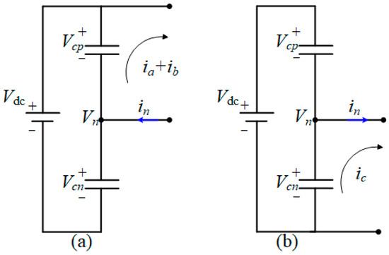
Figure 3.
Effect of the small VV on NPV, with activated at (a) and activated at (b).
In Figure 3, the activation of results in , which corresponds to the discharge of current from capacitor , thereby reducing the . Similarly, for , , indicating that current flows into capacitor , leading to an increase in . Thus, the redundancy of small VVs plays a crucial role in balancing the NPV.
3. Proposed Methodology
This section presents the proposed modulation strategy for the 3L-SNPC inverter, ensuring NPV balance and efficient operation across a full modulation range.
3.1. Region Determination
In three-level inverters (3LIs), voltage levels are typically designed to change only once per VV switching action. This constraint not only reduces switching frequency variation and output harmonics but also significantly lowers computational complexity. Frequent switching actions would require additional calculations and increase the overall computational burden. To address this, each sector in the space vector diagram is systematically divided into four regions to optimize modulation control. As an example, Sector 1 is illustrated in Figure 4, and the same principle is applied to the remaining sectors.
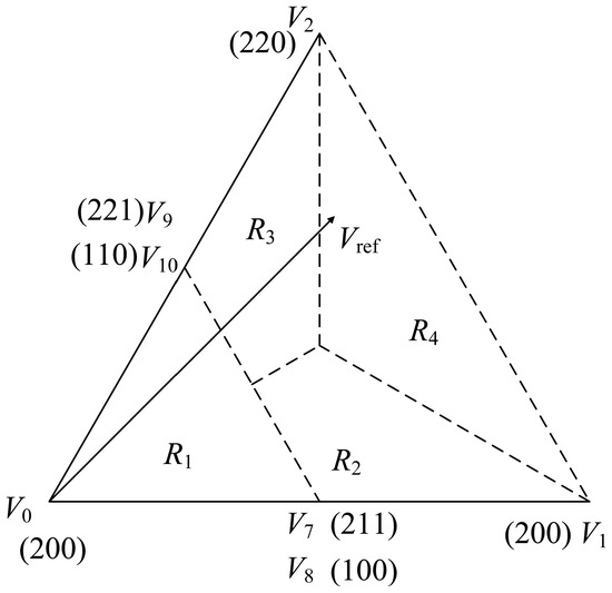
Figure 4.
Region determination in the first sector.
To determine the appropriate region for a given reference VV (RVV), it can be decomposed into its α and β components, denoted as and , where , and . The specific region is then determined based on the values of and . The boundaries between regions are defined as follows:
3.2. Dwell Time Calculation
The dwelling time for the selected VVs can be determined based on their contribution to RVV synthesis. In Sector 1, five VVs are utilized, where each small voltage vector has two redundant switching states. As a result, five distinct duty cycles are defined.
The duty cycle corresponds to the zero-voltage vector . The small voltage vectors and are assigned duty cycles and , respectively. Similarly, the large voltage vectors and are associated with duty cycles and . To ensure proper modulation, each duty cycle must remain within the range of 0 to 1, and their sum must always equal 1.
By following these constraints, the duty cycle of each voltage vector can be uniquely determined after identifying the specific region of RVV within each sector. This process is guided by the voltage-second balance principle, ensuring accurate reference voltage synthesis.
3.2.1. Dwell Time Calculation in
If RVV enters region , the duty cycles of , and are applied on , , and respectively. Since and are not used in this region, their corresponding duty cycles are set to zero, i.e., . The relationship between duty cycles and the components of the reference voltage vector is given by
Solving (7) and (8) results in the following duty cycle expressions:
3.2.2. Dwell Time Calculation in
If RVV is positioned in region , the voltage vectors , , and will be applied with duty cycles , , and , respectively. Consequently, and are set to zero. The relationship between duty cycles and , in this region is given by
Solving (10) while satisfying the constraints in (7) yields the following duty cycle expression:
3.2.3. Dwell Time Calculation in
If RVV is situated in region , the voltage vectors , , and will be applied with duty cycles , , and , respectively. In this case, setting leads to the following relationships:
Solving (12) while considering the constraints in (7) results in the following duty cycle expressions:
3.2.4. Dwell Time Calculation in
If RVV is located in region , the voltage vectors , , , and will be applied with duty cycles , , , and , respectively. In this case, . The following relationships can be established:
Considering (7) and (14), there are four unknown variables but only three relationships, leading to an infinite number of possible solutions. Simplifying (14) using (7) gives
From (15), the following relationship for duty cycles can be derived:
For ease of calculation, define as
To satisfy the duty cycle constraints , , and , the following expressions are obtained:
The duty cycle can then be determined as a function of and :
Substituting and from (19) into (7) yields
Given the constraint , the boundary condition for can be expressed as
There is no fixed constant that satisfies the dynamic boundary condition of . For simplicity, the average of the upper and lower boundaries is chosen. In this case, the average value tends to balance the application of and by adjusting their respective duty cycles and , ensuring both small VVs are applied for sufficient duration during sector selection and transitions. This prevents abrupt switching from large VVs to non-adjacent small VVs when the dwelling time of a small VV is shorter than the system dead time, such as the transition from to . This guarantees a smoother VV transition sequence.
The final expression for is given by
3.3. Carrier-Based Implementation with XOR Gates
Once the duty cycles and switching states have been determined, the next step is to generate gate signals for the 3L-SNPC inverter. Traditional methods often rely on complex sequential programming, where each duty cycle is assigned to its corresponding switching state, resulting in high programming complexity and implementation challenges. To address this issue, a carrier-based implementation method using XOR gates is proposed to simplify the intricate FPGA-based sequential programming process.
The 3L-SNPC inverter consists of five pairs of complementary switches: The front-end dual buck converter includes and , while the back-end 2L-VSI consists of , and . To generate the correct gate signals, five reference values need to be compared with the carrier signal, denoted as , , , , and .
Due to the inherently asymmetric three-phase structure of the 3L-SNPC inverter, directly comparing the reference values with the carrier signal does not produce the correct gate signals. To overcome this challenge, a logic compensatory counter (LCC) is introduced for each reference value to ensure the accurate output of switching states.
For their respective logic operations associated, five LCCs are defined: , , , and , where counters and are required for switches , and , , and are employed to maintain the correct output of the back-end 2L-VSI.
Compared to FPGA-based implementations, XOR logic integrated circuits (ICs) offer a low-cost alternative (<USD 1 per chip), significantly reducing system complexity while maintaining accurate modulation and NPV balancing across the full modulation range. This ensures that the proposed carrier-based XOR implementation provides an efficient and practical solution for real-time control in the 3L-SNPC inverters.
A flowchart of the proposed carrier-based implementation with XOR gates is presented in Figure 5. It generates PWM signals in two stages. The first stage involves comparing reference values and a subset of LCCs with the carrier. The LCCs follow a different comparison logic, and if the counter value exceeds the carrier, a ‘0’ is outputted. This ‘0’ is subsequently used in the XOR logic operation, which follows the logic operation principles , and .
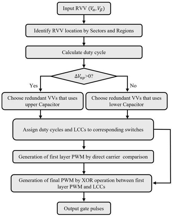
Figure 5.
Flowchart of the proposed carried-based modulation strategy for the 3L-SNPC inverter.
3.4. RVV Sythesization
To synthesize the RVV, only small and zero vectors are employed in , whereas small and large vectors are utilised in , and . Redundant small vectors are employed to balance the NPV, such as , , , and . For instance, and can be used to discharge , while and can be utilised to discharge . Define NPV deviation as .
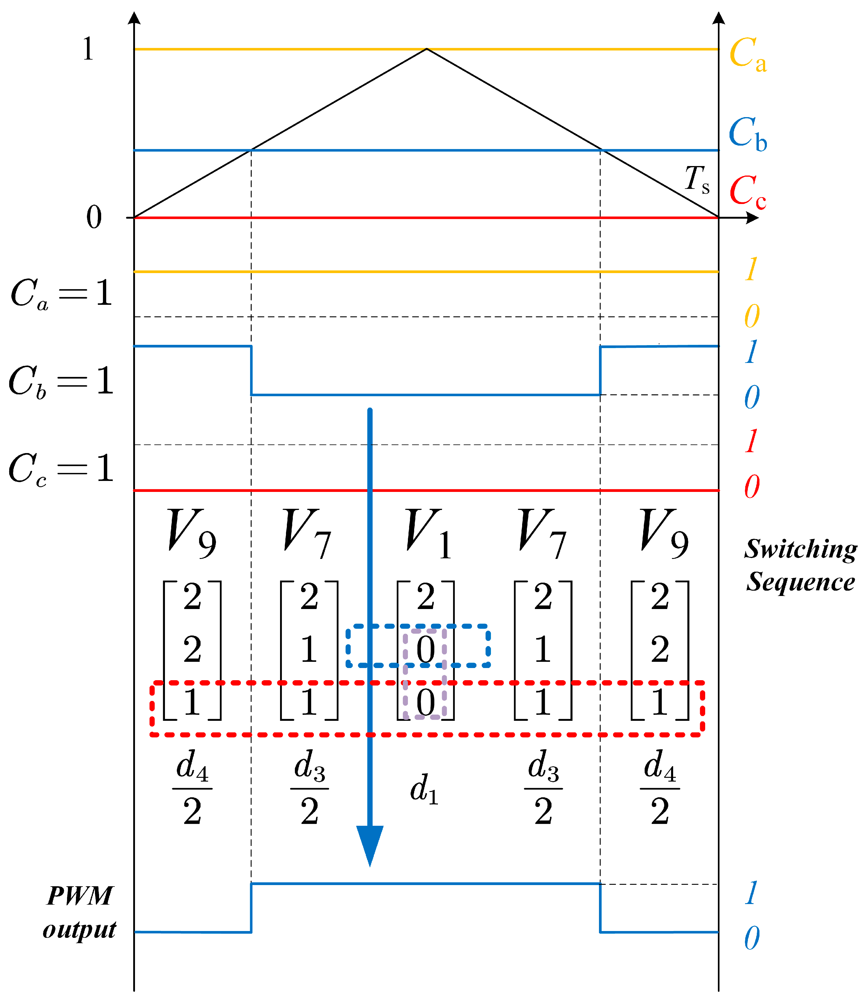
3.4.1. RVV Synthesis in
In , when the neutral point voltage deviation is greater than zero, switches and are activated to balance the NPV. Consequently, the output voltages of the dual buck converter are clamped at and .
In this case, voltage vectors , and are selected. Their corresponding 2L-VSI switching sequence is illustrated in Figure 6. The reference values for the 2L-VSI can be derived as
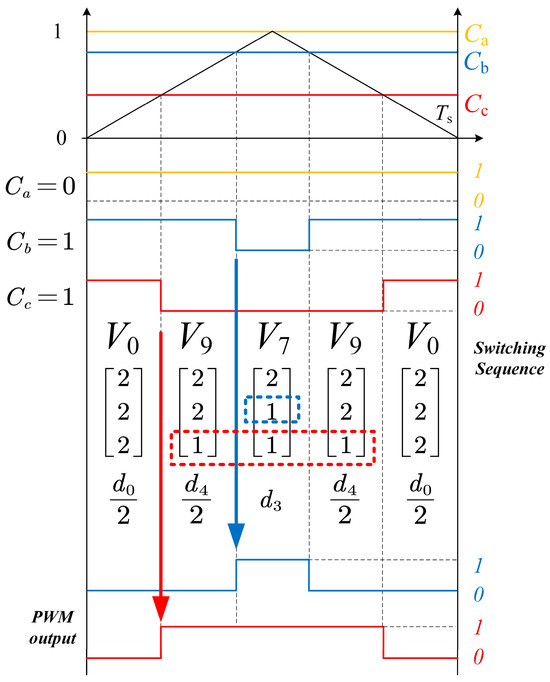
Figure 6.
Switching sequence and gate pulse generation for .
The LCCs for this case are
When is smaller than zero, switches and must be activated to increase . In this scenario, voltage vectors and are selected, following the switching sequence shown in Figure 7. The reference values determined in this case are the same as Equation (23).
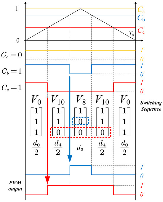
Figure 7.
Switching sequence and gate pulses generation for .
To generate the correct PWM output, the LCCs mentioned in Equation (24) are used; the final PWM output is obtained by
where represents the pulse width modulation signals for the corresponding phase leg, and is generated by comparing the reference value with the carrier. Since the back-end 2L-VSI produces consistent gate signals, any fluctuations in only affect the dual buck converter operation, ensuring smooth transitions.
3.4.2. RVV Synthesis in and
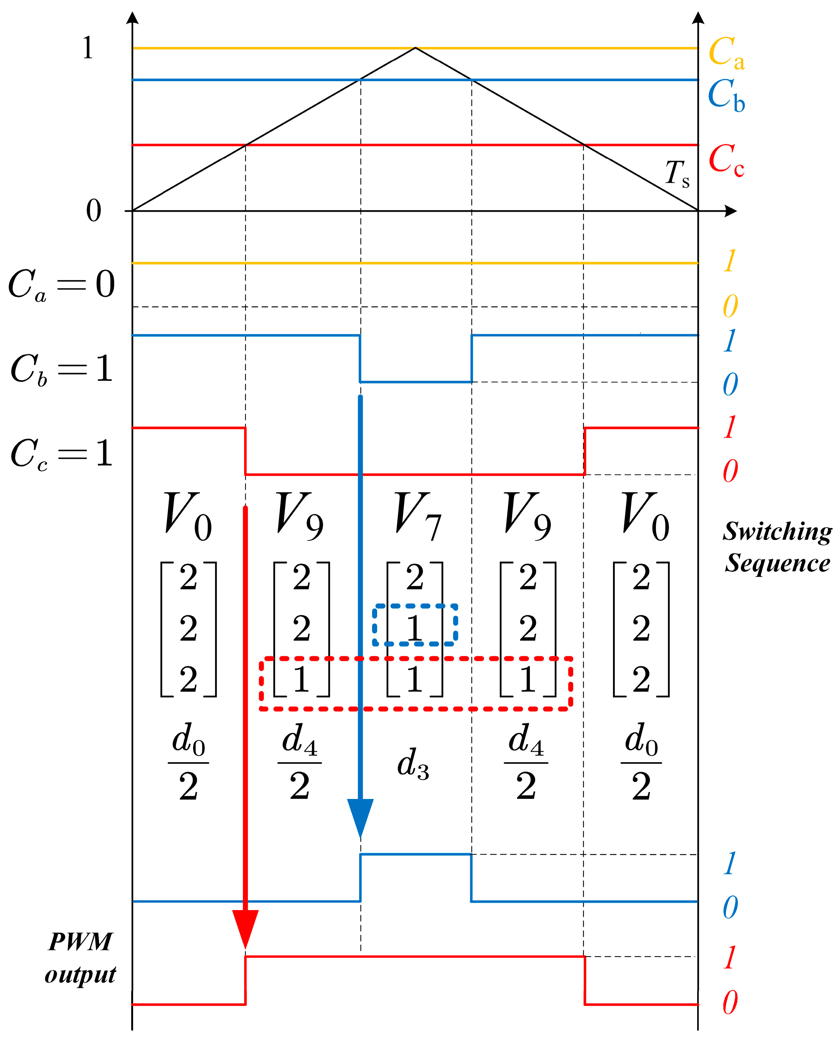
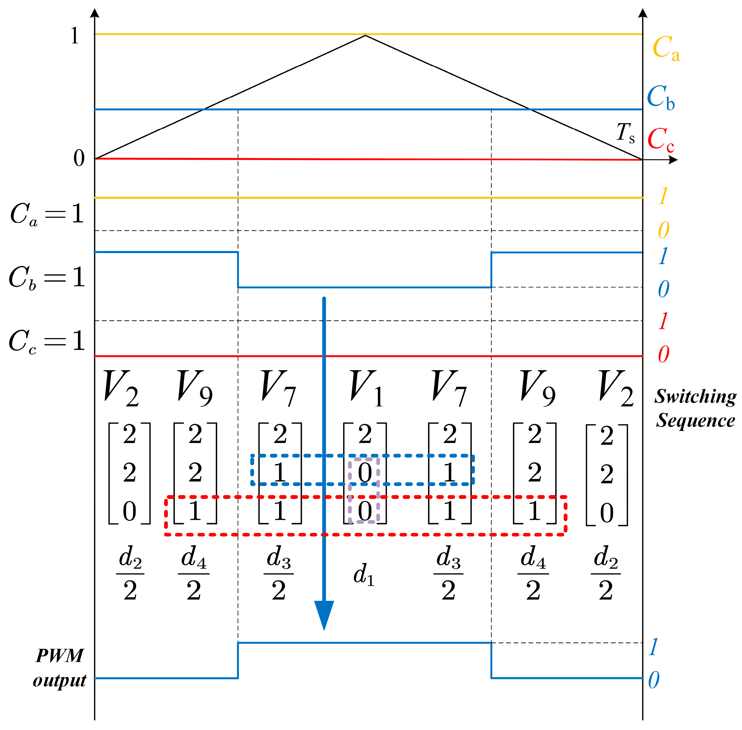
In , when is greater than zero, voltage vectors , and are selected. The inverter switching sequence is shown in Figure 8.

Figure 8.
Switching sequence and gate pulse generation for .
Since voltage level ‘2’ is used for the dual buck converter, . Additionally, switch conducts only when the voltage level transitions to zero, leading to . Thus, the following combination is applied:
The methodology for vector synthesis in is a similar logic to . For simplicity, further elaboration is omitted herein.
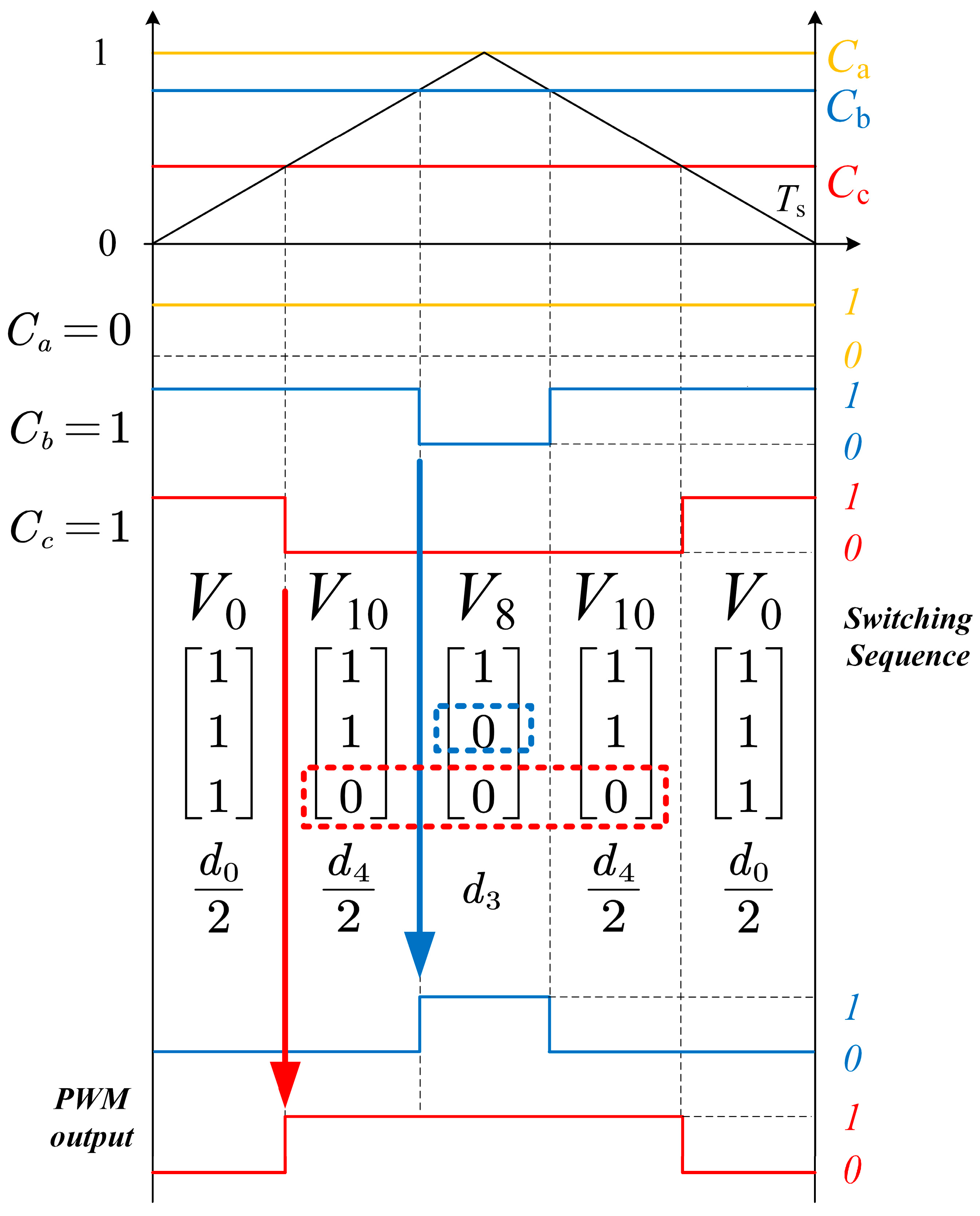
3.4.3. RVV Synthesis in
In , two large vectors are used for vector synthesis. The LCCs of the dual buck converter participate in the modulation process, acting similarly to the duty cycle that is compared with the carrier signal to produce PWM LCC signals. The gate signal for the front-end dual buck converter is obtained using XOR logic operations between the first-layer PWM signal against the PWM LCC signals. The PWM output is then expressed as
where its complement generates the PWM output for . When is positive, the switching sequence at this region results in the same 2L-VSI reference values, as shown in Equation (26). For the dual buck converter, switch remains always ON, so . However, for , the desired switching sequence is neither 0-1-0 nor 1-0-1. To address this, LCC is assigned to , yielding
where gate pulse generation in this region is shown in Figure 9.
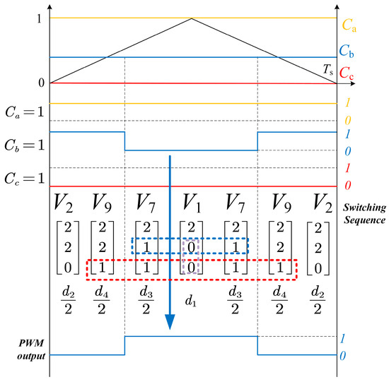
Figure 9.
Switching sequence and gate pulse generation for .
3.5. Overmodulation Consideration
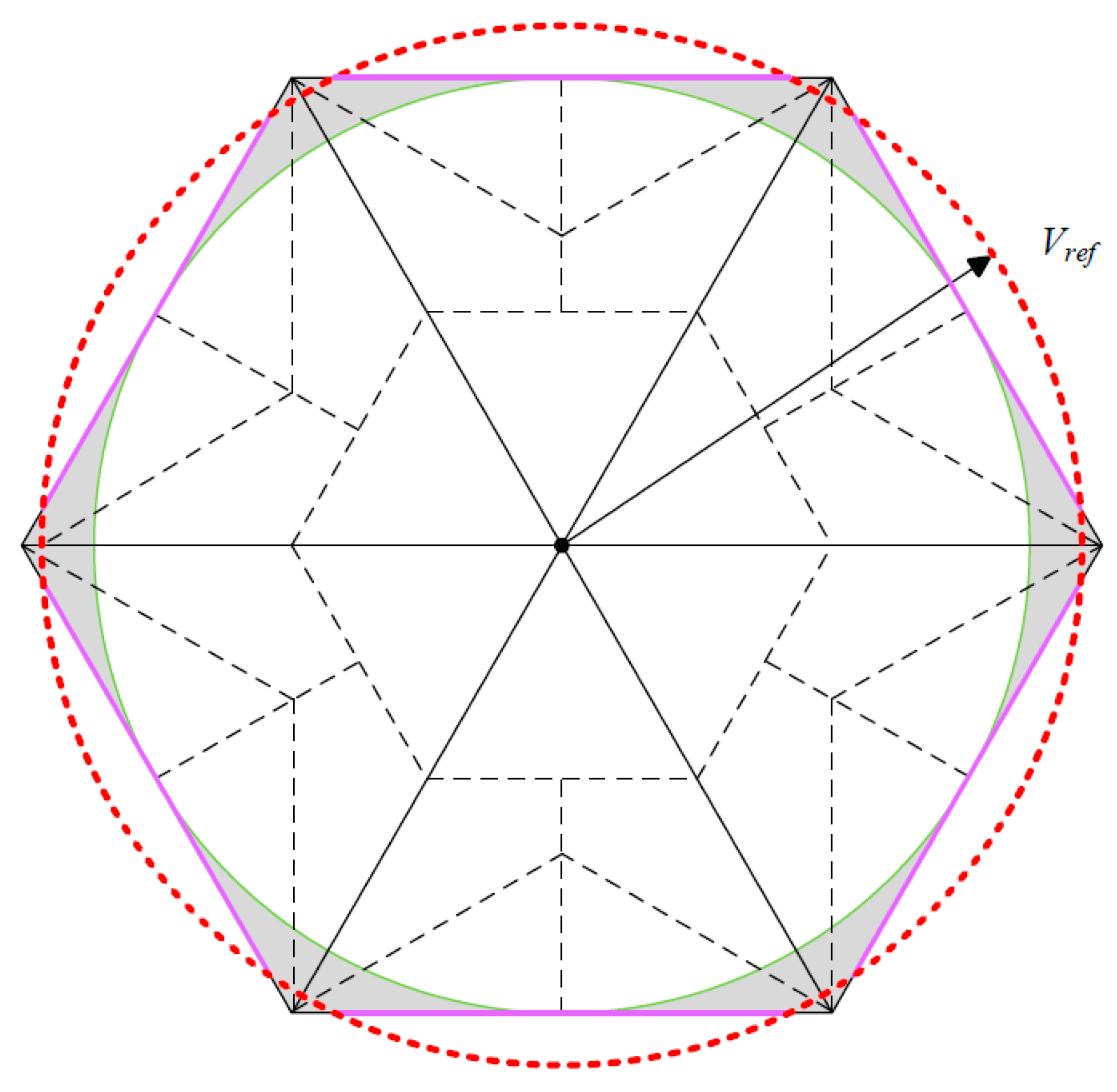
When the modulation index lies within the range of 0 to 0.866, the inverter operates in the linear modulation region. In this region, the RVV remains within the inscribed circle of the outer hexagon of the space vector diagram, as shown in Figure 10, and can be synthesized by the proposed method straight away. The outer hexagon boundary represents the theoretical limit of space vector modulation. The area between the inscribed circle and the hexagon boundary, which is shaded in grey in the figure, is not covered by linear modulation.
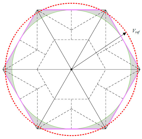
Figure 10.
Schematic of the reference voltage vector in the overmodulation region.
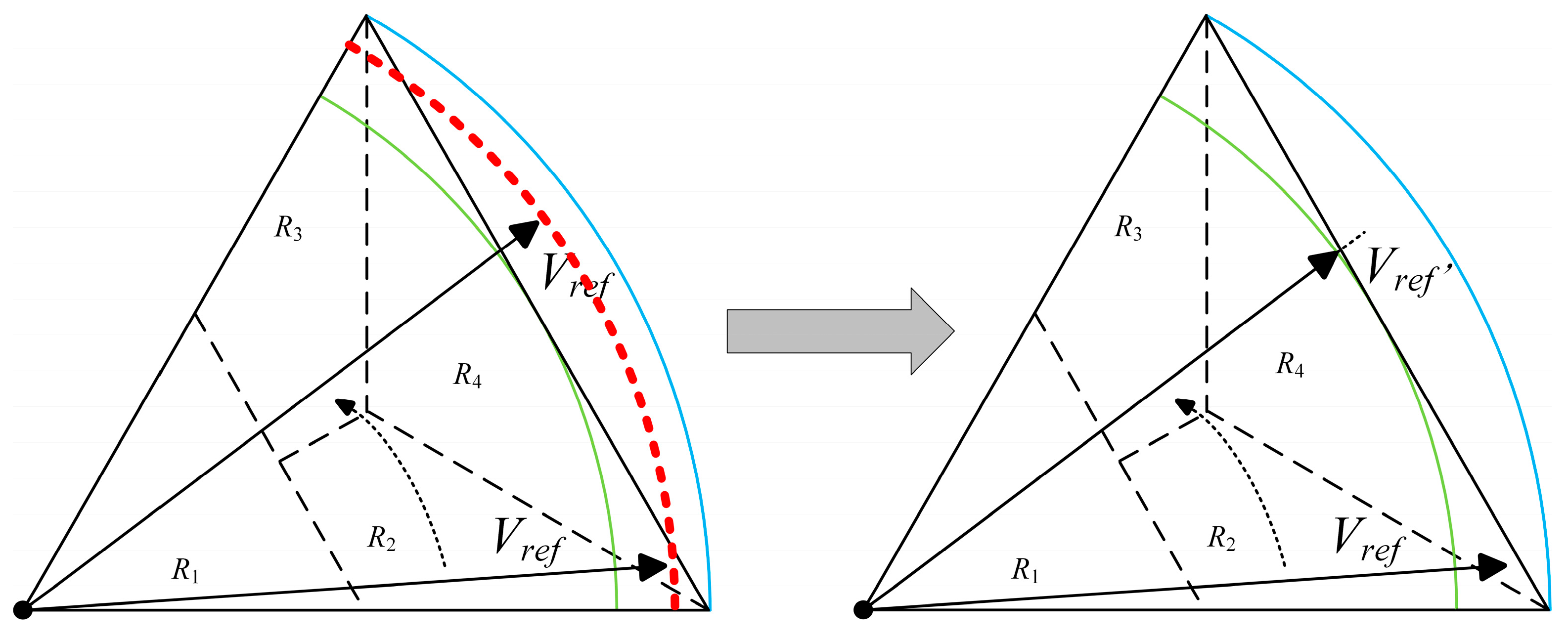
When the modulation index goes beyond 0.866, reaching values between 0.866 and 1, the (RVV) moves into the overmodulation region, which is located between the inscribed circle and outer hexagon and can be represented by the red dashed circle in Figure 10. In this region, the proposed method employs a minimum phase angle error approach to handle the overmodulation challenge [29,30]. Specifically, when the RVV exceeds the outer hexagon boundary, it is projected back onto the boundary while maintaining the same phase angle (), as illustrated in Figure 11. This approach successfully extends the proposed method to achieve overmodulation for the 3L-SNPC inverter.
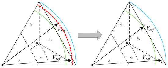
Figure 11.
Operation under overmodulation region.
4. Experimental Results
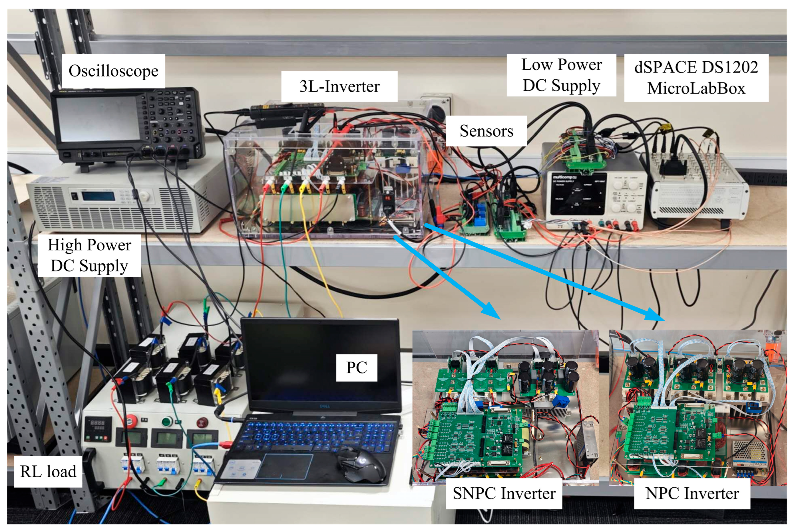
To validate the proposed methodology, experimental setups of both the 3L-SNPC and 3L-NPC inverters are built, as depicted in Figure 12. The system parameters are detailed in Table 3. The proposed method is implemented on the NXP QorIQP5020 processor in the dSPACE DS1202 MicroLabBox with a control period and sampling period of 200 . Carrier frequency is set to 5 kHz. Both inverter platforms use an Infineon FF100F12RT4 IGBT module with the same driver and sampling circuit.
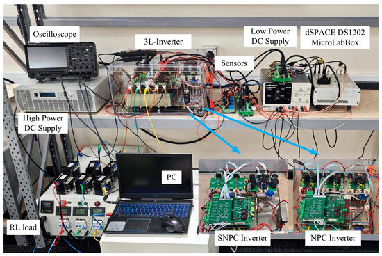
Figure 12.
Experiment platform overview.
Table 3.
Experiment parameters.
4.1. Execution Time
The execution time of the proposed method is measured to test its computational complexity in the 3L-SNPC inverter compared to the 3L-NPC inverter. In this case, the modulation method is written in C language and implemented on a DSP TMS320F28335 with a clock frequency of 150 MHz. A digital output port of a DSP is utilized to measure the execution time. Specifically, the level of the digital output port is set to 5 V when modulation starts and reset to 0 V when execution is finished. The results of the proposed method in comparison to state-of-the-art methods and traditional methods are shown in Table 3.
Table 4 shows that the proposed method achieves a shorter execution time than both the traditional and state-of-the-art methods. In the 3L-SNPC inverter, it reduces the execution time to 7.34 , outperforming the method in [27] (10.05 ) and matching performance against the method in [18] (7.39 ). However, unlike [18], which requires additional FPGA hardware, the proposed method only uses XOR logic gates, making it more cost-effective. For the 3L-NPC inverter, the proposed method also outperforms the traditional method (21.5 ) and achieves comparable performance to state-of-the-art methods.
Table 4.
Execution time of different modulation methods.
The proposed method reduces computational complexity and eliminates FPGA dependency on hardware implementation of 3L-SNPC inverters, making it a faster and more cost-effective solution for real-time DSP-based inverter control.
4.2. Performance Comparison
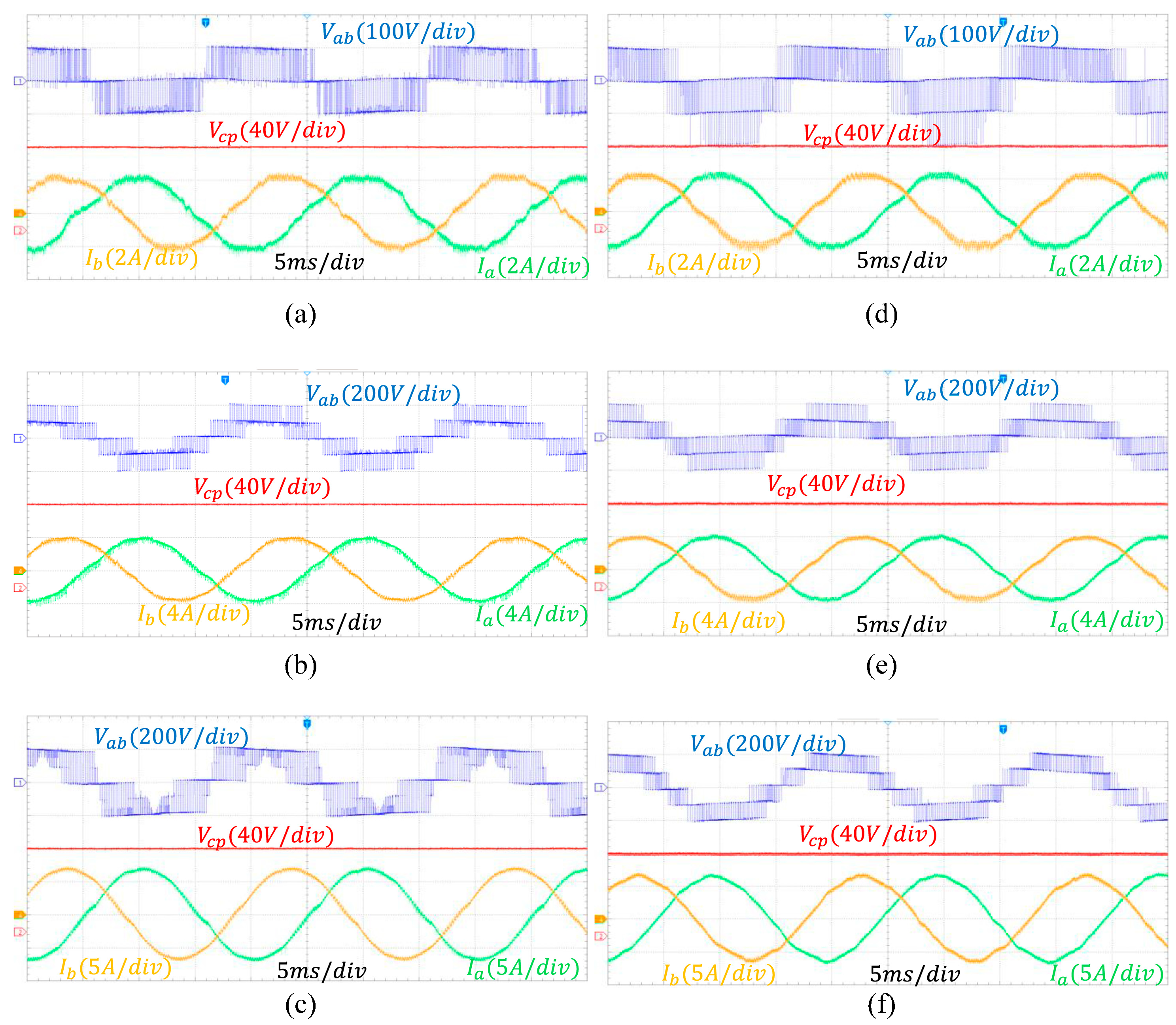
Experimental observations, including the line voltage , the voltage across the upper capacitor , and the phase currents and , are presented in Figure 13. The modulation index, defined as , varied from 0 to 0.866. For modulation indices of 0.3, 0.5, and 0.866, the proposed method for the 3L-SNPC inverter demonstrated an output waveform performance comparable to the same method used in the 3L-NPC inverter.
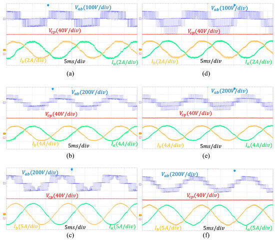
Figure 13.
Experiment results of line voltage , capacitor voltage , line currents and , with modulation index at (a,d) m = 0.3, (b,e) m = 0.5, (c,f) m = 0.866. Left hand side: (a–c) 3L-SNPC inverter results. Right hand side: (d–f) 3L-NPC inverter results.
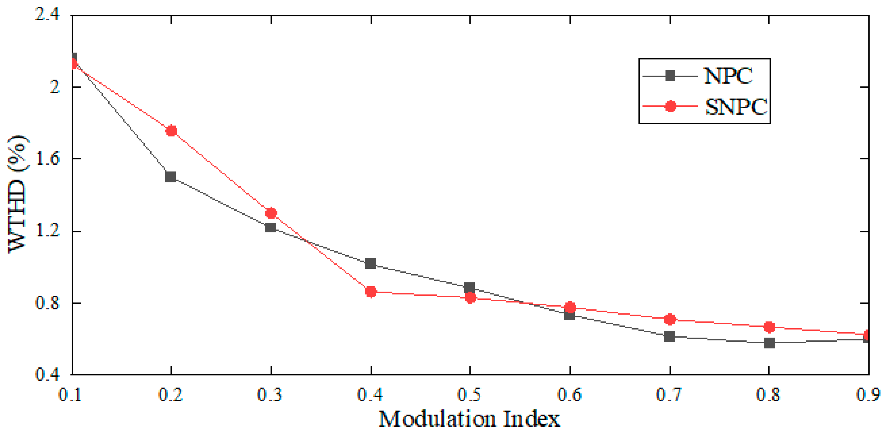
To further evaluate waveform quality, the weighted total harmonic distortion (WTHD) of the line voltage is calculated for various modulation indices, as illustrated in Figure 14. WTHD provides a more robust evaluation metric compared to total harmonic distortion (THD), which is easily influenced by load characteristics and the effectiveness of the filter parameters. The use of WTHD ensures that its weighted values are independent of filter parameters, allowing for a fair comparison to rule out the external circuit influences.
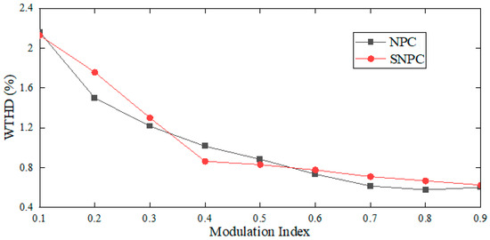
Figure 14.
WTHD of the 3L-NPC and 3L-SNPC inverter.
At lower modulation indices, both the 3L-SNPC and 3L-NPC inverters operate closer to the inner hexagon of the space vector diagram, sharing the same space vector distribution of voltage vectors (VVs). As a result, their output performance in this region is similar. However, at modulation indices of 0.2 and 0.3, the WTHD of the 3L-SNPC inverter is slightly higher than that of the 3L-NPC inverter by 0.25% and 0.12%, respectively. This occurs because, during reference VV synthesis, the effective allocation time for selected VVs is minimal, making dead-time a significant factor in increasing the harmonic distortion. This effect is more pronounced in the 3L-SNPC inverter due to its three-phase asymmetric circuit structure.
As the modulation index increases, the influence of harmonics diminishes, and the WTHD of the 3L-SNPC inverter shows a reduction of 0.15% and 0.06% compared to the 3L-NPC inverter.
Under heavy load conditions, the WTHD of the 3L-SNPC inverter is slightly higher than that of the 3L-NPC inverter by 0.09–0.02%. The absence of six medium VVs in the 3L-SNPC inverter, compared to the 3L-NPC inverter, limits its ability to accurately approximate the reference VV. However, as the operating region approaches the outer hexagon of the SVM diagram and the output current amplitude increases, the selected VVs have a longer effective duration, reducing harmonics caused by IGBT dead-time.
Higher current amplitudes at elevated modulation indices generally result in increased inverter losses. However, the 3L-SNPC inverter has the potential for lower losses due to its reduced component count. To further investigate this aspect, switching loss tests are conducted for both inverters.
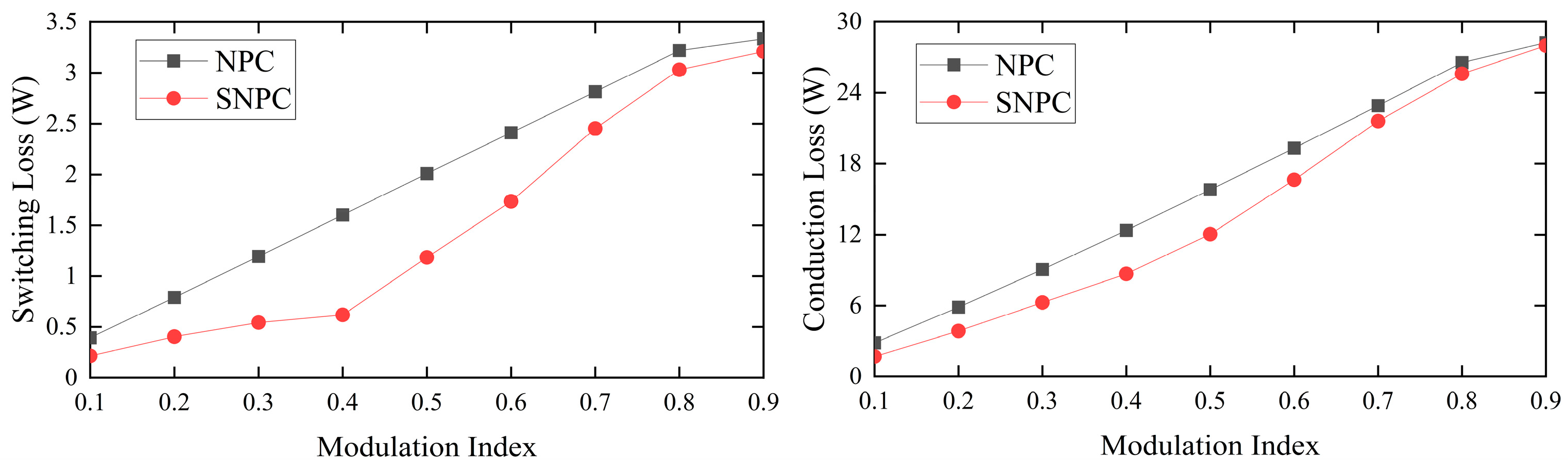
4.3. Loss Analysis
The switching losses are assessed using double-pulse test (DPT) experiments, consisting of a half-bridge module identical to that used in the inverter, a variable air-core inductor, and a DSP development board. The measured waveforms are shown in Figure 15. Following the methodology described in [10], the switching and conduction losses are quantified under various operating conditions, with voltages ranging from 100 V to 200 V and currents from 1 A to 10 A.
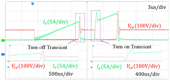
Figure 15.
Double-pulse test result with denoting voltage across collector and emitter; represents emitter current.
Figure 15 demonstrates that the 3L-SNPC inverter, utilizing the proposed CB-SVM, incurs lower switching and conduction losses compared to the conventional 3L-NPC inverter across the entire modulation spectrum.
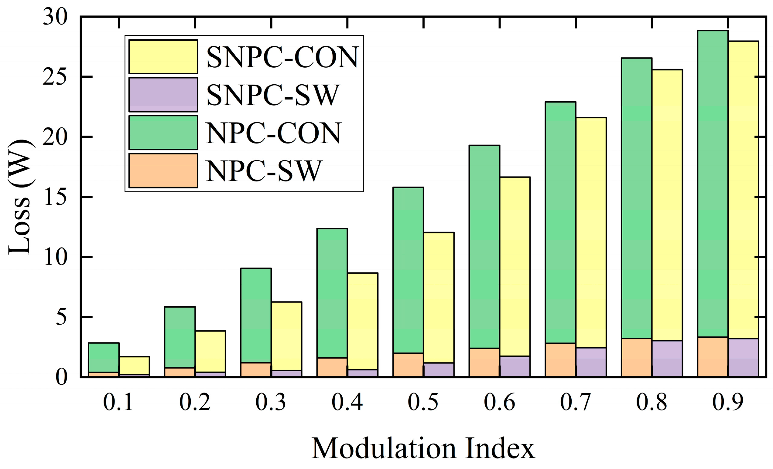
Figure 16 and Figure 17 demonstrate the loss characteristics of the proposed modulation method implemented in the 3L-SNPC and 3L-NPC inverter. In summary, these findings confirm that the proposed CB-SVM method, when applied to the 3L-SNPC inverter, maintains comparable voltage and current waveform quality while achieving reduced inverter losses relative to the conventional 3L-NPC inverter.
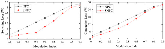
Figure 16.
Switching and conduction loss comparison for the 3L-SNPC and the 3L-NPC inverter under the proposed method.

Figure 17.
Total loss comparison with switching loss and conduction loss for the 3L-SNPC and the 3L-NPC inverter under the proposed method.
5. Simulation Results
To further validate the performance of the proposed modulation strategy, simulations were conducted and compared with two state-of-the-art methods under two operating conditions in Table 5 and Table 6. The modulation index was tested from 0.1 to 1.0; the WTHD of line voltage and the loss of the inverter from switching and conducting actions of IGBT are recorded. Power loss was estimated through a co-simulation framework combining MATLAB/Simulink and PLECS, where empirical switching and conduction loss data derived from double-pulse test (DPT) experiments were embedded into the loss models.
Table 5.
Simulation results of state-of-the-art methods compared to the proposed method under .
Table 6.
Simulation results of state-of-the-art methods compared to the proposed method under .
It can be seen from Table 5 and Table 6 that for each method, the WTHD results under the two operating conditions are nearly the same. This shows that using line voltage WTHD is a more stable and fair way to compare different modulation methods because it is less affected by filter or load parameters. This also gives better guidance for practical use and engineering evaluation.
As for comparative performance, the proposed method outperforms both reference methods in WTHD when the modulation index exceeds 0.6. At lower modulation indices, it achieves better performance than Method 2 and delivers comparable results to Method 1. In terms of execution time, measured experimentally, the proposed method achieves lower latency than Method 1 and comparable speed to Method 2. Most notably, the hardware implementation cost of the proposed strategy is significantly reduced. It requires only a single XOR logic gate IC, while Method 1 relies on an FPGA-based sequence control, and Method 2 requires FPGA or CPLD support, resulting in considerably higher hardware complexity and cost. In summary, the proposed method achieves a favorable balance between modulation performance, computational complexity, and hardware cost, making it a highly attractive solution for real-time low-cost multilevel inverter applications.
6. Conclusions
This paper presented a low-cost carrier-based SVPWM strategy for the 3L-SNPC inverter, aiming to simplify implementation by replacing FPGA/CPLD with XOR logic gates. The proposed method achieved a minimum WTHD of 0.40% at full load condition, reduced inverter loss, and shortened execution time to 7.34 μs, demonstrating comparable or superior performance to existing methods via different working conditions. These results confirm its effectiveness and cost-efficiency. Future work will explore advanced control algorithms based on the proposed modulation to further enhance performance.
Author Contributions
Conceptualization, Z.L. and X.Z.; methodology, Z.L.; software, Z.L.; validation, Z.L., W.D. and Y.B.; formal analysis, Z.L.; writing—original draft preparation, Z.L.; writing—review and editing, X.Z., H.H.C.I. and T.F. All authors have read and agreed to the published version of the manuscript.
Funding
This work is supported by Future Battery Industries Cooperative Research Centre (FBI-CRC) Microgrid Battery Deployment project under grant number 55002200 as part of the Australian Government Cooperative Research Centres Program.
Data Availability Statement
The original contributions presented in this study are included in the article. Further inquiries can be directed to the corresponding author(s).
Conflicts of Interest
The authors declare no conflicts of interest.
Abbreviations
The following abbreviations are used in this manuscript:
| 3L-SNPC | Three-level simplified neutral point clamped inverter |
| 3L-NPC | Three-level neutral point clamped inverter |
| 2LI | Two-level inverter |
| CB-SVPWM | Carrier-based space vector pulse width modulation |
| WTHD | Weighted total harmonics distortion (%) |
| THD | Total harmonics distortion (%) |
| NPV | Neutral point voltage |
| VVs | Voltage vectors |
| CPLD | Complex programmable logic device |
| FPGA | field-programmable gate array |
References
- Nadh, G.; Rahul, S.A. Clamping Modulation Scheme for Low-Speed Operation of Three-Level Inverter Fed Induction Motor Drive with Reduced CMV. IEEE Trans. Ind. Appl. 2022, 58, 7336–7345. [Google Scholar] [CrossRef]
- Payami, S.; Behera, R.K.; Iqbal, A. DTC of Three-Level NPC Inverter Fed Five-Phase Induction Motor Drive with Novel Neutral Point Voltage Balancing Scheme. IEEE Trans. Power Electron. 2018, 33, 1487–1500. [Google Scholar] [CrossRef]
- Mukundan, C.M.N.; Jayaprakash, P.; Subramaniam, U.; Almakhles, D.J. Binary Hybrid Multilevel Inverter-Based Grid Integrated Solar Energy Conversion System with Damped SOGI Control. IEEE Access 2020, 8, 37214–37228. [Google Scholar] [CrossRef]
- Hamid, R.T.; Danny, S.; Kashem, M.M.; Ciufo, P. Solar PV and Battery Storage Integration usinga New Configuration of a Three-Level NPCInverter with Advanced Control Strategy. IEEE Trans. Energy Convers. 2014, 29, 354–365. [Google Scholar]
- Choudhury, A.; Pillay, P.; Williamson, S.S. DC-Link Voltage Balancing for a Three-Level Electric Vehicle Traction Inverter Using an Innovative Switching Sequence Control Scheme. IEEE J. Emerg. Sel. Top. Power Electron. 2014, 2, 296–307. [Google Scholar] [CrossRef]
- Pan, D.; Zhang, D.; He, J.; Immer, C.; Dame, M.E. Control of MW-Scale High-Frequency “SiC+Si” Multilevel ANPC Inverter in Pump-Back Test for Aircraft Hybrid-Electric Propulsion Applications. IEEE J. Emerg. Sel. Top. Power Electron. 2021, 9, 1002–1012. [Google Scholar] [CrossRef]
- Zhang, D.; He, J.; Pan, D. A Megawatt-Scale Medium-Voltage High-Efficiency High Power Density “SiC+Si” Hybrid Three-Level ANPC Inverter for Aircraft Hybrid-Electric Propulsion Systems. IEEE Trans. Ind. Appl. 2019, 55, 5971–5980. [Google Scholar] [CrossRef]
- Chavali, R.V.; Dey, A.; Das, B. A Hysteresis Current Controller PWM Scheme Applied to 3-Level NPC Inverter for Distributed Generation Interface. IEEE Trans. Power Electron. 2021, 37, 1486–1495. [Google Scholar] [CrossRef]
- Lee, J.-H.; Lee, J.-S.; Moon, H.-C.; Lee, K.-B. An Improved Finite-Set Model Predictive Control Based on Discrete Space Vector Modulation Methods for Grid-Connected Three-Level Voltage Source Inverter. IEEE J. Emerg. Sel. Top. Power Electron. 2018, 6, 1744–1760. [Google Scholar] [CrossRef]
- Ahmed, M.H.; Wang, M.; Hassan, M.A.S.; Ullah, I. Power Loss Model and Efficiency Analysis of Three-Phase Inverter Based on SiC MOSFETs for PV Applications. IEEE Access 2019, 7, 75768–75781. [Google Scholar] [CrossRef]
- Belkhode, S.; Rao, P.; Shukla, A.; Doolla, S. Comparative Evaluation of Silicon and Silicon-Carbide Device-Based MMC and NPC Converter for Medium-Voltage Applications. IEEE J. Emerg. Sel. Top. Power Electron. 2022, 10, 856–867. [Google Scholar]
- Schweizer, M.; Kolar, J.W. Design and Implementation of a Highly Efficient Three-Level T-Type Converter for Low-Voltage Applications. IEEE Trans. Power Electron. 2013, 28, 899–907. [Google Scholar] [CrossRef]
- Klumpner, C.; Lee, M.; Wheeler, P. A New Three-Level Sparse Indirect Matrix Converter. In Proceedings of the IECON 2006—32nd Annual Conference on IEEE Industrial Electronics, Paris, France, 6–10 November 2006. [Google Scholar]
- Rojas, R.; Ohnishi, T.; Suzuki, T. Simple structure and control method for a neutral-point-clamped PWM inverter. In Proceedings of the Conference Record of the Power Conversion Conference, Yokohama, Japan, 19–21 April 1993. [Google Scholar]
- Xiang, C.; Ouyang, Z.; Zhang, X.; Iu, H.H.C.; Cheng, S. An Improved Predictive Current Control of Eight Switch Three-Level Post-Fault Inverter with Common Mode Voltage Reduction. IEEE Trans. Circuits Syst. I Regul. Pap. 2022, 69, 3861–3872. [Google Scholar]
- Ngo, T.; Foo, G.; Baguley, C. A predictive torque control strategy for interior permanent magnet synchronous motors driven by a three-level simplified neutral point clamped inverter. In Proceedings of the IECON 2016—42nd Annual Conference of the IEEE Industrial Electronics Society, Florence, Italy, 24–27 October 2016. [Google Scholar]
- Guo, X.; Liu, M.; Guan, J.; Chen, C.; Kang, Y.; Li, R.; Li, P.; Cai, J.; Jin, X.; Chen, J.; et al. Analysis and Solution of Voltage Overshoot of Keep-Off State Devices in Three Level Simplified Neutral Point Clamped Inverter. In Proceedings of the 2022 IEEE 3rd China International Youth Conference on Electrical Engineering (CIYCEE), Wuhan, China, 3–5 November 2022. [Google Scholar]
- Foo, G.H.B.; Ngo, T.; Zhang, X.; Rahman, M.F. SVM Direct Torque and Flux Control of Three-Level Simplified Neutral Point Clamped Inverter Fed Interior PM Synchronous Motor Drives. IEEE/ASME Trans. Mechatron. 2019, 24, 1376–1385. [Google Scholar] [CrossRef]
- Jing, M.; Xing, X.; Li, X.; Zhang, R.; Jiang, Y.; Zhang, C. Virtual Vector Based Model Predictive Control for Three-Level Sparse Neutral Point Clamped Inverter. In Proceedings of the 2021 IEEE International Conference on Predictive Control of Electrical Drives and Power Electronics (PRECEDE), Jinan, China, 20–22 November 2021. [Google Scholar]
- Zhang, X.; Foo, G.H.B.; Jiao, T.; Ngo, T.; Lee, C.H.T. A Simplified Deadbeat Based Predictive Torque Control for Three-Level Simplified Neutral Point Clamped Inverter Fed IPMSM Drives Using SVM. IEEE Trans. Energy Convers. 2019, 34, 1906–1916. [Google Scholar]
- Sheianov, A.; Xiao, X.; Sun, X. Adaptive Dead-Time Compensation for High-Frequency Three-Level Sparse NPC Inverter. IEEE J. Emerg. Sel. Top. Power Electron. 2023, 11, 5169–5182. [Google Scholar]
- Ngo, T.; Foo, G.; Baguley, C.; Mohan, D. A novel direct torque control strategy for interior permanent magnet synchronous motors driven by a three-level simplified neutral point clamped inverter. In Proceedings of the 2016 IEEE Energy Conversion Congress and Exposition (ECCE), Milwaukee, WI, USA, 18–22 September 2016. [Google Scholar]
- Wang, C.; Zhong, Q.-C.; Zhu, N.; Chen, S.-Z.; Yang, X. Space Vector Modulation in the 45° Coordinates α′β′ for Multilevel Converters. IEEE Trans. Power Electron. 2021, 36, 6525–6536. [Google Scholar] [CrossRef]
- Chamarthi, P.; Chhetri, P.; Agarwal, V. Simplified Implementation Scheme for Space Vector Pulse Width Modulation of n-Level Inverter with Online Computation of Optimal Switching Pulse Durations. IEEE Trans. Ind. Electron. 2016, 63, 6695–6704. [Google Scholar]
- Sun, Q.; Wang, Z.; Sharkh, S.M.; Hao, W. A Flexible and Decoupled Space Vector Modulation Scheme with Carrier-Based Implementation for Multilevel Converters. IEEE Trans. Power Electron. 2023, 38, 8135–8149. [Google Scholar]
- Sun, Q.; Sharkh, S.M.; Wang, Z.; Wang, Z.; Shi, G. Space Vector Modulation with Common-Mode Voltage Elimination and Switching Frequency Minimization for Multilevel Converters. IEEE Trans. Power Electron. 2024, 39, 7952–7967. [Google Scholar] [CrossRef]
- Zhang, D.; Cittanti, D.; Sun, P.; Huber, J.; Bojoi, R.I.; Kolar, J.W. Detailed Modeling and In-Situ Calorimetric Verification of Three-Phase Sparse NPC Converter Power Semiconductor Losses. IEEE J. Emerg. Sel. Top. Power Electron. 2023, 11, 3409–3423. [Google Scholar] [CrossRef]
- Wang, F.; Li, Z.; Tong, X. Modified Predictive Control Method of Three-Level Simplified Neutral Point Clamped Inverter for Common-Mode Voltage Reduction and Neutral-Point Voltage Balance. IEEE Access 2019, 7, 119476–119485. [Google Scholar] [CrossRef]
- Guo, F.; Yang, T.; Diab, A.M.; Yeoh, S.S.; Li, C.; Bozhko, S. An Overmodulation Algorithm with Neutral-Point Voltage Balancing for Three-Level Converters in High-Speed Aerospace Drives. IEEE Trans. Power Electron. 2021, 37, 2021–2032. [Google Scholar] [CrossRef]
- Jing, R.; Zhang, G.; Wang, G.; Bi, G.; Ding, D. An Overmodulation Strategy Based on Voltage Vector Space Division for High-Speed Surface-Mounted PMSM Drives. IEEE Trans. Power Electron. 2022, 37, 15370–15381. [Google Scholar] [CrossRef]
- Huang, L.; Wang, Y.; Zhou, H.; Chen, X.; He, S.; Zhang, X.; Yuan, J. Simplified SVPWM Algorithm for Three-Level NPC Converter Based on Virtual Chopping. IEEE J. Emerg. Sel. Top. Power Electron. 2024, 12, 3740–3749. [Google Scholar] [CrossRef]
- Yan, Q.; Zhou, Z.; Wu, M.; Yuan, X.; Zhao, R.; Xu, H. A Simplified Analytical Algorithm in abc Coordinate for the Three-Level SVPWM. IEEE Trans. Power Electron. 2021, 36, 3622–3627. [Google Scholar] [CrossRef]


Disclaimer/Publisher’s Note: The statements, opinions and data contained in all publications are solely those of the individual author(s) and contributor(s) and not of MDPI and/or the editor(s). MDPI and/or the editor(s) disclaim responsibility for any injury to people or property resulting from any ideas, methods, instructions or products referred to in the content. |
© 2025 by the authors. Licensee MDPI, Basel, Switzerland. This article is an open access article distributed under the terms and conditions of the Creative Commons Attribution (CC BY) license (https://creativecommons.org/licenses/by/4.0/).