Abstract
Recently, multiple new technologies have emerged for automating the development of neural network (NN) accelerators for both field-programmable gate arrays (FPGAs) and application-specific integrated circuits (ASICs). This paper explores methodologies for translating NN algorithms into chip layouts, with a focus on end-to-end automation, cost-effectiveness, and open-source software. We present a robust framework for developing NN-to-silicon solutions and demonstrate a seamless plug-and-play automation flow using TensorFlow, Vivado HLS, HLS4ML, and Openlane2. SkyWater Technologies’ 130 nm PDK (Sky130) is employed to successfully generate layouts for two small NN examples under 1000 parameters, incorporating dense, activation, and 2D convolution layers. The results affirm that current open-source tools effectively automate low-complexity neural network architectures and deliver faster performance through FPGA structures. However, this improved performance comes at the cost of increased die area compared to bare-metal designs. While this showcases significant progress in accessible NN automation, achieving manufacturing-ready layouts for more complex NN architectures remains a challenge due to current tool limitations and heightened computational demands, which points to exciting opportunities for future advancements.
Keywords:
automation; artificial intelligence; open-source; NN accelerator; CNN; FPGA; HLS; ASIC; Sky130; OpenLane 1. Introduction
Artificial intelligence (AI) chips are specialized alternatives to generic CPUs, often designed to handle parallel processing and equipped with their own memory and I/O systems. A key feature of AI chips is the implementation of structures tailored to handle the matrix operations common in neural networks (NNs); these structures are known as NN accelerators [1]. In numerous applications, the optimization of reduced size and power consumption is a critical design consideration, although not invariably mandatory. The reduction in these parameters can significantly enhance the efficiency and applicability of technologies, particularly in contexts where minimizing the physical footprint and power usage is crucial for overall system performance and user accessibility. For instance, Internet of Things (IoT) devices in remote locations require low power consumption for prolonged operation [2], while wearable technologies like fitness trackers need compact, energy-efficient designs for comfort and extended use [3]. In medical applications, such as wireless capsule endoscopy [4], an ultra-low-power edge computing system is critical for diagnosing gastrointestinal diseases in real time.
Compared to conventional commercial solutions and programmable platforms, ASICs generally exhibit reduced area requirements and significantly lower power consumption, which are critical for extending battery life and enabling long-term operation in energy-constrained environments. While not an exact comparison, a frequently cited paper by Kuon and Rose [5] highlights the substantial disparity between FPGAs and ASICs. Their research indicated that, on average, FPGAs were 21 times larger in area, 2.8 times slower, and consumed 9 times more power compared to ASICs, primarily due to the generic nature of FPGA circuitry. A recent literature supports these findings; for instance, the ASIC-based AccelTran accelerator achieved 372,000 GOPs, drastically surpassing the top FPGA implementation (Me-ViT at 2682 GOPs). Similarly, ASIC-based DTQAtten delivered an energy efficiency of 1298 GOPs/W, while FPGA-based BETA reached only 174 GOPs/W, underscoring ASICs’ significant advantages in both performance density and energy efficiency due to their specialized architectures and optimized manufacturing processes [6].
The potential of open-source technology for ASIC development is primarily twofold: (1) cost reduction and (2) experimental flexibility. With the advent of open-source PDKs and the increasing maturity of free EDA tools, the development of production-ready ASICs without incurring software costs has become more feasible. This development facilitates broad collaboration—analogous to that observed in the software domain—among senior engineers, researchers, students, and enthusiasts, and provides unrestricted access to the field of microchip design. A notable example is [7], where undergraduate students successfully leveraged the SkyWater 130 nm Technology (Sky130) and an open-source EDA flow to tape out a processor in a single semester. In essence, this represents an emerging area with the potential to impact both individual microchip design projects and the field as a whole.
Another noteworthy example is the Ecko project, an open-source initiative that leverages automated, community-driven methodologies for NN accelerator design. Utilizing publicly available tools, the Ecko initiative provides detailed resources, including documentation, methodologies, and practical examples for automating the transition from neural network algorithms to silicon implementation. By emphasizing transparency and accessibility, Ecko exemplifies how modern open-source projects can significantly streamline the NN-to-ASIC development workflow, thereby fostering collaboration and innovation across academia and industry [8].
This paper aims to investigate open-source tools for ASIC design, specifically to generate the NN accelerator component of an AI chip using a high-level programming environment. The objective is to establish the foundation for future custom AI systems. This research distinguishes itself from similar work through the utilization of the FPGA tool HLS4ML, adopting an FPGA-inspired approach to ASIC AI chip design.
2. The Open-Source Landscape for NN-to-Silicon
In essence, four essential components are needed for creating open-source ASIC NN accelerators.
- Programming environment for creating an NN;
- Creating the corresponding circuit equivalent of an NN;
- Designing the layout of the circuit equivalent;
- The choice of process node.
While these components could be managed manually, the ideal flow aims to establish a streamlined process that automates as many individual components as feasible. This approach seeks to reduce factors such as time-to-market, speed up prototyping, and ensure functionality by applying criteria throughout the development process. The current state-of-the-art solutions in this space utilize different tools, albeit with the same goal, to address these challenges.
2.1. The State of the Art in NN-to-Silicon Solutions
The following presents the recent open-source frameworks and workflows created by researchers to address ASIC AI chip development. First, the 2021 method, VeriGOOD-ML, is a no-human-in-the-loop methodology for generating machine-learning-optimized Verilog from a given ONNX file [9]. It addresses various key challenges in creating hardware descriptions for ML algorithms and layout designs for both small and simple and large and complex networks. Esmaeilzadeh et al. adopted a platform-based approach, categorizing ML algorithms into three separate groups and choosing different approaches for each. For non-DNN ML algorithms, they utilized the template-based framework TABLA by Mahajan et al. [10], specifically designed to simplify the development process of NN accelerators for FPGAs, focusing on supervised learning algorithms (both classification and regression). For DNN algorithms, they used their own compiler, GeneSys, which translates an ONNX description into a new graph description. During this transformation, the compiler can replace the original nodes with template optimizations for common DNN structures, such as dense, convolution, and various activation layers. The result is a hardware-aware reconstruction that, for example, builds a binary tree for the L2 norm or optimizes data flow for convolutions. Finally, for small specific ML algorithms, they employed their own compiler named Axiline, a hard-coded engine designed for specific small ML algorithms. The rationale is that, for certain commonly used ML algorithms, investing time in complex computations from scratch, as in the TABLA or GeneSys cases, may not be a worthwhile investment. This method can thereby increase developer productivity in specific cases. The paper demonstrates successful layout generation for classic ML algorithms, namely an SVM, ResNet50, and a logistic regression algorithm, as a proof of concept on the GF12LP 13 metal layer technology using all 13 layers. This achievement was accomplished using a blend of commercial and open-source automation tools for tasks such as place-and-route, CTS, and PDN generation.
Second, the 2022 method, SODA-Opt, by Agostini et al., is an open-source framework that generates NN-optimized hardware descriptions for implementation in either FPGA or ASIC designs [11]. Similar to VeriGOOD-ML, it follows the approach of converting popular file formats (demonstrated with both TensorFlow and PyTorch) to layout through an intermediate step of converting the model from Python/ONNX to an optimized equivalent. This equivalent is then processed by an HLS tool to create Verilog, and ultimately goes through the RTL-GDSII tool OpenROAD. In contrast to VeriGOOD-ML’s platform-based design, Agostini et al. chose to design a single compiler: the SODA compiler. This compiler translates the Python NN algorithm into efficient machine code using the MLIR framework found in the LLVM project. This framework allows for reconstructing code on a compiler level. They utilized MLIR’s built-in dialects (through intermediate representations) to turn the high-level NN code into corresponding hardware-optimized machine code equivalents. This is achieved through loop optimizations such as tiling and unrolling, and redundancy optimizations such as early alias analysis (EAA) and dead code elimination (DCE). The result is a highly optimized equivalent of the input NN algorithm that can then be passed to the open-source HLS tool PandaBambu, distributed by Politecnico Milano. As an HLS tool, Bambu can synthesize both C/C++ code and MLIR intermediate representations (which can be compiled through C compilers such as GoLang) into corresponding Verilog/VHDL. Bambu comes with built-in verification tools for simulation and analysis, similar to those found in software like Xilinx’s Vivado. A LeNet CNN was transformed from Python code to a layout on the open-source theoretical 45nm FreePDK design kit using OpenROAD.
Third, the 2023 method, although not released in a paper, was developed by Baungarten et al., the winners of the Efabless 2023 contest [12]. Their project, called AI-by-AI, attempts to create as many parts of an NN accelerator as possible using AI technologies [13]. Specifically, they used the LLM ChatGPT4 as the primary development tool. Using ChatGPT4, they managed to generate an MNIST CNN in TensorFlow (Python) with 96.87% accuracy, then generate a function for reducing precision in the CNN to 16-bit, and then translate these layers into Vivado HLS-compatible C equivalents by step-by-step prompting the creation of a bare-metal CNN forward function. They then fed the quantized, bare-metal C code to Vivado HLS, generated the corresponding Verilog RTL, and processed it through OpenLane (an automation fork of OpenROAD), creating the corresponding layout on the production-ready Sky130 PDK. Using Efabless’ SoC template with full I/O (called Caravel), the entire AI chip was created.
2.2. FPGA as Part of NN-to-Silicon Solutions
A late 2023 survey by Ferrandi et al. that summarizes design methodologies to accelerate deep learning mentions most of the aforementioned tools [14]. One tool mentioned for its potential, but not yet adopted by any current state-of-the-art methods, is HLS4ML, an open-source FPGA tool designed for NN-to-C++ interpretation. It supports multiple HLS back-ends, such as the aforementioned Vivado HLS used in AI-by-AI and the open-source Vitis HLS.
Due to the feedforward nature of CNN data flow, it lends itself well to efficient hardware structures, especially when considering that 90% of operations in general NN accelerators are matrix multiplications and convolutions. As a result, developing efficient topologies for handling matrix multiplications becomes a primary focus of optimization [15]. Multiple architectural approaches can achieve the same output from a given input, albeit with distinct hardware implementations. Consequently, many researchers advocate for a co-design strategy, where the NN’s architecture and its feasibility for hardware implementation (both FPGAs and ASICs) are given equal consideration [16].
It is also noted that none of the aforementioned workflows experiment with newer NN developments specifically tailored for FPGAs. Considering that FPGA NN accelerators are a well-studied domain, there may be advantages found that could assist in the HLS process and the overall flow.
2.3. NN Accelerators on FPGA
The NN accelerator architecture of the CNN utilizes the FPGA by distributing the heavy use of multiplications across parallel resources [17]. Initially, this was carried out by assigning DSPs to each node, resulting in a considerable number of float multipliers for larger networks. Over time, this method has been replaced by more contemporary approaches to designing NNs for FPGAs, pioneered in 2020 by Wang et al. and later refined in 2023 [18,19]. LUTnet is a methodology for FPGA NN optimizations.
On the FPGA, the modern optimization flow is as follows:
- Hardware-aware NN model: Designing, training, testing, and pruning NNs are performed using TensorFlow, with deliberate reductions in the total number of parameters in the NN, at the cost of some accuracy.
- From DNN to BNN: [17] The optimization on the FPGA itself involves transforming the weights and biases of the NN into binarized versions, reducing computational complexity. This is accomplished through a combination of Python scripts and HLS tools.
- From logic gates to LUTs: By replacing as many conventional multipliers (DSPs) with LUTs as possible, it has been shown that the circuit complexity and footprint are reduced. As a result, there is less fan-in (i.e., fewer inputs) at summation points, saving area and resources compared to using DSPs in an equivalent scenario.
- Training on FPGA: An additional benefit is that LUTs can be updated on the FPGA, enabling backpropagation and allowing for hardware-specific training.
For performance validation, the efficiency of hardware resource usage and circuit latency are simple measures that most consider. Four key parameters are (1) reuse, i.e., whether blocks are single-use or reusable in the circuitry; (2) latency, i.e., accounting for gate delay and other factors; (3) power consumption; and (4) area.
The relationship between hardware-specific parameters leads to a trade-off between parallelism (to achieve low latency, low reuse factors are required) and size (high reuse factors result in higher latency). In FPGAs, the speed of memory access is a bottleneck for many NN accelerators when latency is of particular importance [15].
2.4. FPGA Advancement for ASIC Design
As significant efforts have been dedicated in recent years to optimizing NNs for FPGA platforms, particularly focusing on hardware-aware implementation, it raises the question of whether these advancements can be applied in an ASIC context. When an LUT is translated for ASIC implementation, it results in a circuit composed of gates. This brings up the question: what is the purpose of employing LUTs initially? Despite this transition, there are still compelling reasons to explore this approach in ASIC development.
Firstly, integrating FPGA testing into the ASIC development process can offer an additional layer of testing and validation as the resources needed to test NNs on FPGA platforms are considerably lower.
Secondly, LUTs on FPGAs are adaptable, enabling backpropagation and facilitating hardware-specific training. This makes them one level closer to representative hardware compared to CPU/GPU platforms.
Thirdly, although ASIC implementation removes the programmable aspect inherent in FPGAs, it does not preclude their utilization. With emerging advancements, such as the work by Amarú et al. in 2021 [20], which outlines an LUT-based optimization methodology customized for ASIC synthesis rather than FPGAs (further refined in 2022 [21]), this approach could potentially become prevalent.
2.5. Common Patterns in NN-to-Silicon Solutions
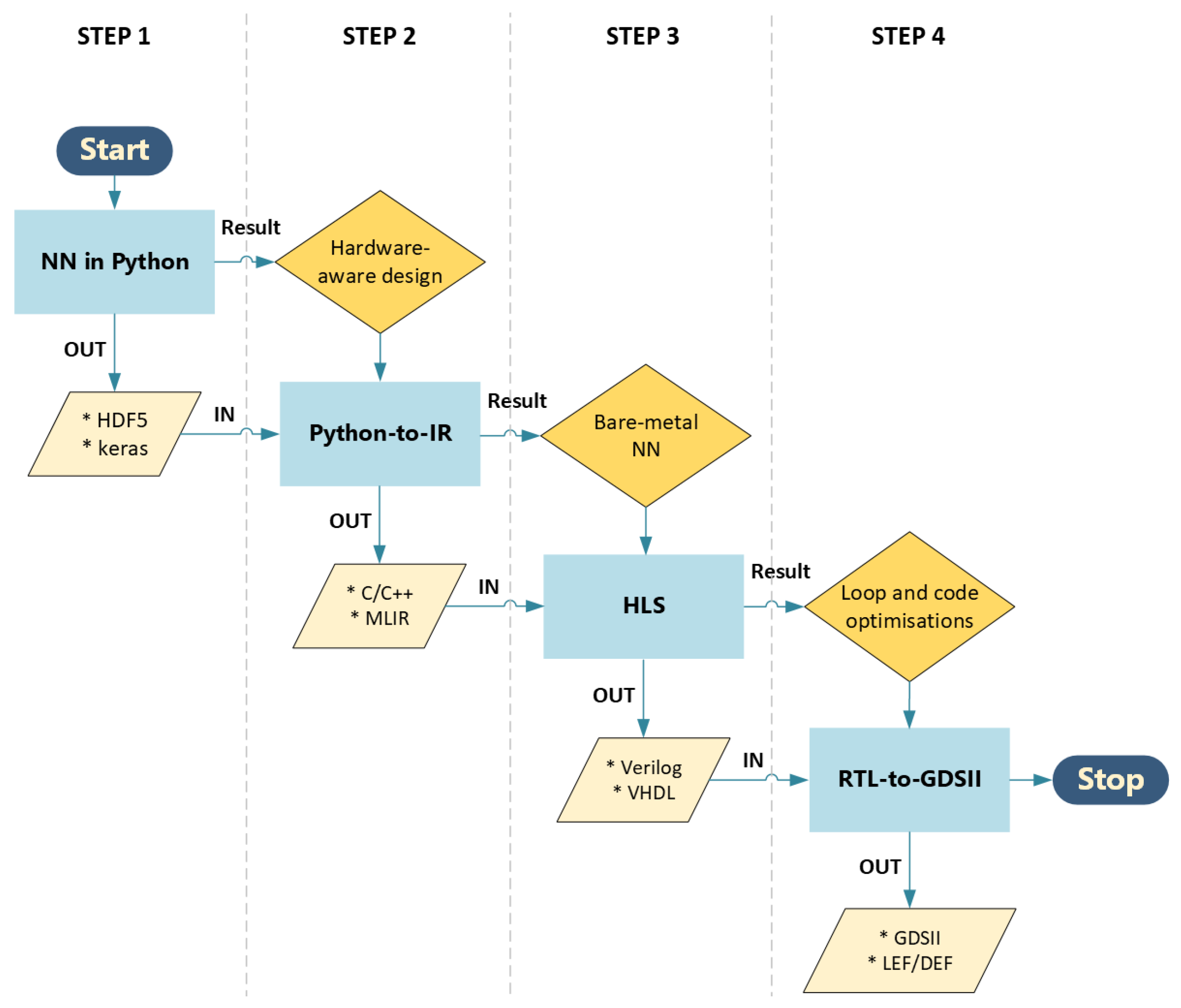
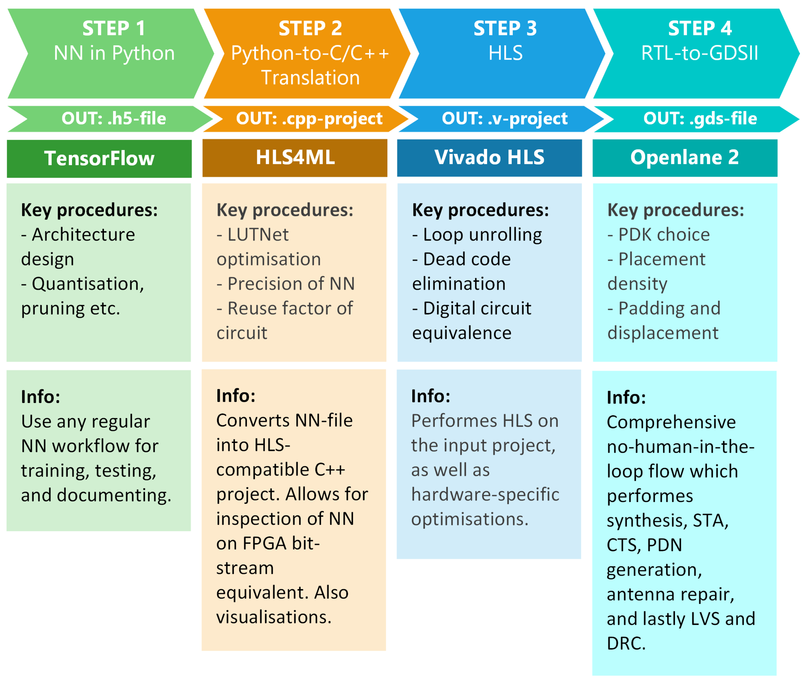
Breaking down VeriGOOD-ML, SODA-Opt, and AI-by-AI into their essential components reveals some common patterns and a conceptual framework from which novel methods can be developed (see Figure 1).

Figure 1.
Flowchart of the conceptual flow, with processes on top (denoted with results) and proposed output file formats indicated by “*” in the boxes at the bottom (denoted with IN/OUT).
- NN in Python: While there is no standardized approach for creating neural networks, using a Python environment aligns with the preference of most developers.
- Translation of Python to IR: This step serves as an intermediate process for HLS to Verilog/VHDL. Synthesis from C/C++ is currently the most common approach. Significant progress has been made in code conversion tools that employ libraries of code blocks. Additionally, language translation tools, including those powered by large language models like ChatGPT, alongside various online platforms, offer efficient services in this field.
- HLS: Required for utilization of the most popular RTL-GDSII suites, HLS tools often include hardware-aware optimizations and relevant testing procedures, thus introducing an additional assessment before layout creation. This step can potentially leverage existing tools for FPGA technology, enabling comprehensive verification and testing for timing/delay and resource utilization.
- RTL-GDSII: The automation of routing and component placement is well explored in the field of digital circuitry. Additionally, open-source tools like ’Magic’ and Klayout are available for DRC and LVS verification. OpenROAD also allows for the extraction of parasitics, the output of LEF/DEF files, and the generation of heat maps and congestion maps for further analysis before production.
Each of these steps can be regarded as an individual component, akin to black boxes, with well-defined input/output relationships. This modular structure allows for the seamless integration of future technologies in place of existing components if necessary. These four steps highlight how separate tools designed to accomplish very specific goals can operate cohesively in this context.
3. Implementation
An experiment was conducted using a conceptual flow template with tools including TensorFlow, HLS4ML, Vivado HLS, and Openlane2. An overview of this experiment is provided in Figure 2. The roles of each open-source tool in the proposed automation flow are clearly delineated as follows: TensorFlow provides a versatile Python-based platform for neural network creation, training, and evaluation, enabling rapid prototyping. HLS4ML converts these high-level neural network models into hardware-optimized C++ code suitable for synthesis. Vivado HLS translates this intermediate representation into synthesizable Verilog RTL, enabling detailed hardware-specific optimization. Finally, Openlane2 automates the RTL-to-GDSII layout process, including placement, routing, and verification, thereby facilitating a streamlined progression from high-level models to fabrication-ready layouts. The GitHub repository [22] contains all the necessary files to run the experimental flow and an installation guide for the tools used.
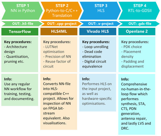
Figure 2.
The structure of the experimental flow. This Python-based approach utilizes (1) TensorFlow, (2) HLS4ML, (3) Vivado HLS, and (4) Openlane2. All relevant files for running the same flow, as well as an installation guide, can be found on the attached GitHub [22].
3.1. Python Emphasis
The technologies were selected with compatibility in mind. They all work seamlessly with any Python-compatible IDE. Vivado HLS can be invoked via the CLI within a Python script, and Openlane2 allows for the customization of layout parameters, such as floorplanning, using Python scripting.
3.2. Package Version Considerations
At the time of writing, the steps utilize the latest releases of most software packages. TensorFlow, HLS4ML, and Openlane2 are all at their latest versions, regularly updated with new features. Vivado HLS is version 2020.1, as currently supported by HLS4ML.
3.3. NN Architecture
The flow was tested on three networks. One tested whether it was possible to complete the flow on a simple dense and activation layer, functioning as a template example that can be run multiple times an hour for debugging (henceforth referred to as ‘Debug template’).
Inspired by both AI-by-AI and MobileNet, two additional template examples were created:
- Baseline: The NN model from AI-by-AI, using the grayscale MNIST dataset with a clock frequency of 40 MHz. The CNN from Baumgarten et al., given its detailed specifications, is used as a baseline to test whether the FPGA-optimized flow can perform at the same level on the same PDK.
- Compatibility: We selected a wireless capsule endoscopy application as our target. To gauge compatibility with real-world models, we used a neural network inspired by the wireless endoscopy capsule, featuring separable convolution layers and batch normalization. This model processes 32 × 32 pixel, 3-channel images from the CIFAR10 dataset. Conceptually similar to MobileNet but with reduced complexity, this CNN model served as a practical benchmark.
The chosen architectures were selected to test both the flow’s compatibility with future NN accelerator design and whether the flow could produce a complete NN accelerator end-to-end.
4. Results
The following is a summary of the produced results and relevant findings.
4.1. Debug Template
The debug template primarily demonstrated the following:
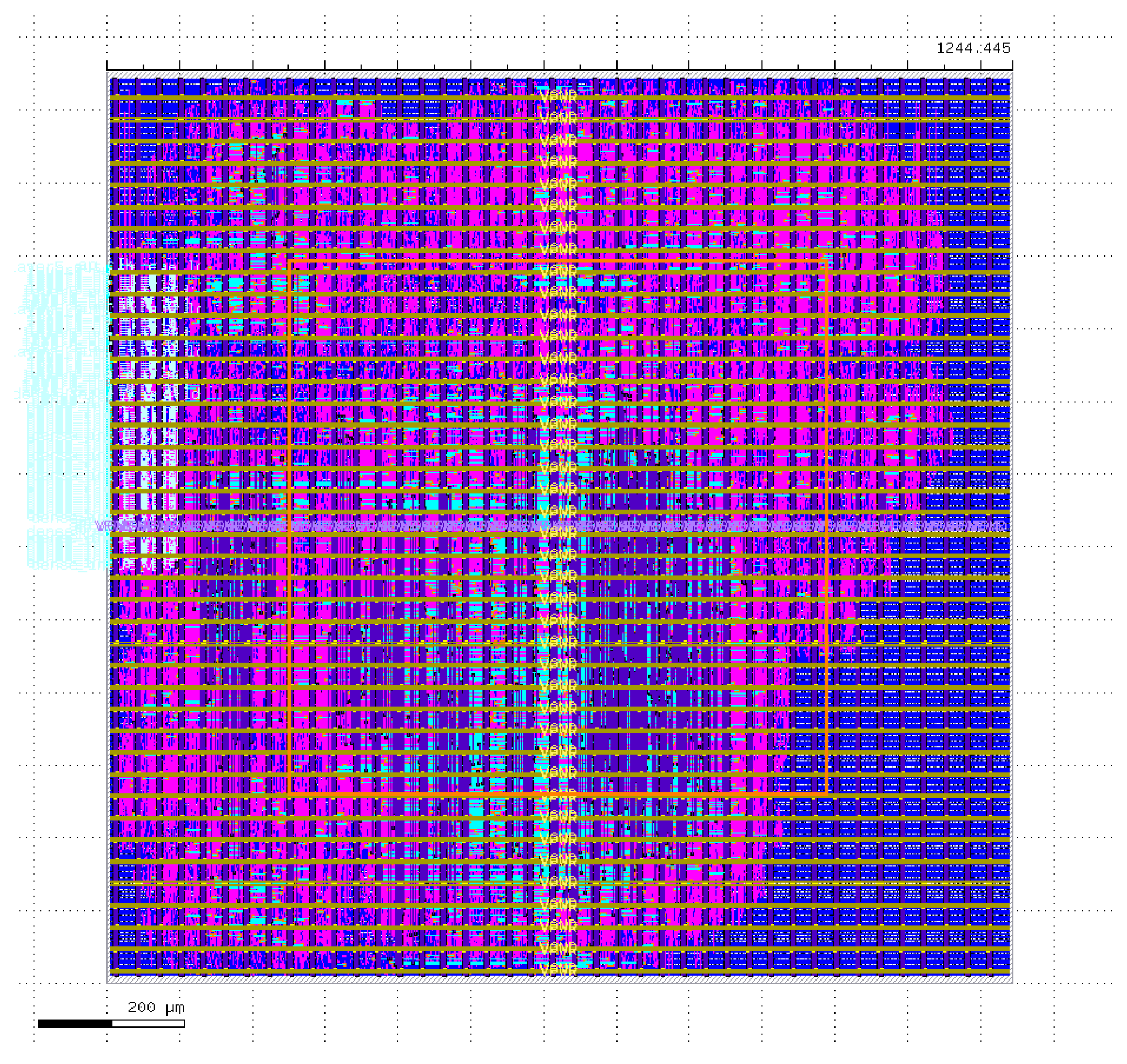
- It is possible to complete the flow on a very simple architecture with the current setup and produce a corresponding layout (Figure 3).
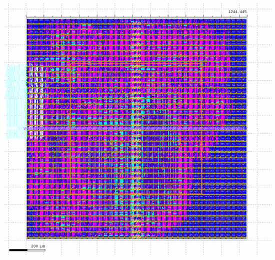 Figure 3. Openlane2-generated error-free layout for the debug template with 75% pruning and a reuse factor of 16. The layout dimensions are µm, utilizing all 5 metal layers of the Sky130 PDK. All the I/O is on the left-hand side.
 - The tools used in Flow 1 provide ample individual validation methods that can be used to address problems throughout the four automation phases.
- The FPGA-targeted HLS4ML can automate the creation of dense and activation layers.
- Openlane2 provides extensive documentation on layout violations and includes tools to address these violations, resulting in an error-free layout.
- It was possible to generate a layout for the debug template with 75% pruning and a reuse factor of 16, on a µm area, utilizing all five metal layers of the Sky130 PDK.
4.2. Baseline NN
The baseline NN primarily demonstrated the following:
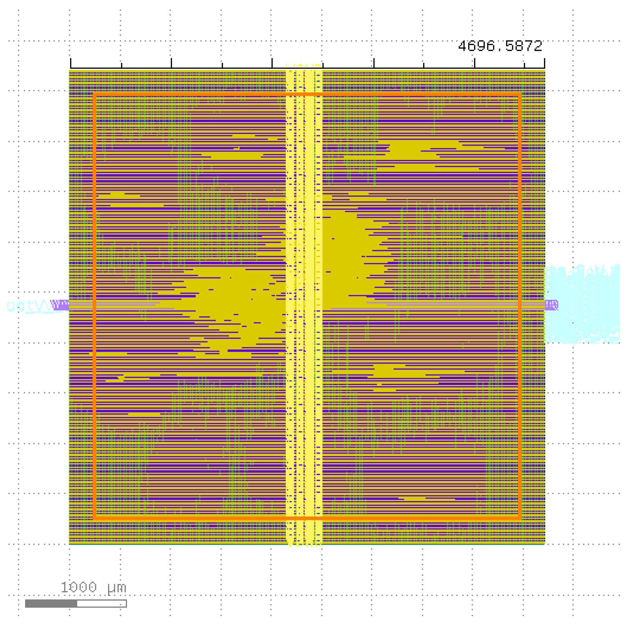
- It was possible to complete the floorplanning phase of a simple CNN architecture with the current setup (see Figure 4); however, extracting reports for layout violations was not possible.
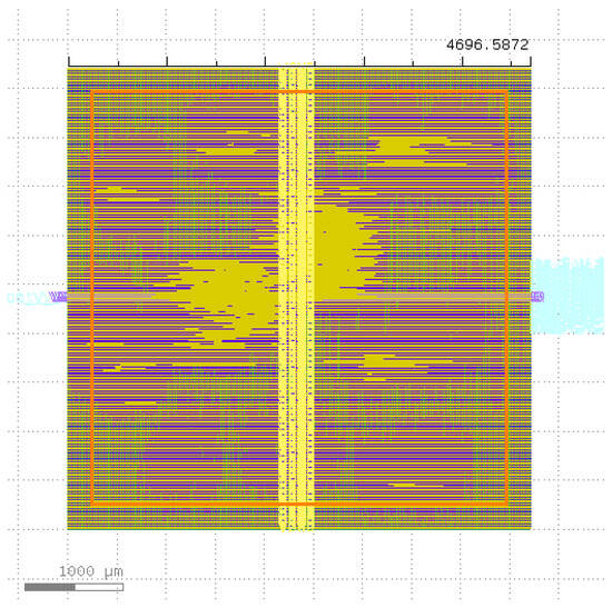 Figure 4. Openlane2-generated layout for the baseline template with a reuse factor of 16. Its dimensions are µm. Due to data being streamed in, there is one 16-bit input to the first convolutional layer, with a 16-bit output for each of the 10 classes of the MNIST dataset.
 - The FPGA-targeted HLS4ML is not optimal for saving area. Although the model was already small and multipliers were heavily reused (with a reuse factor of 16), it resulted in a die area 234.83% larger than AI-by-AI’s bare-metal implementation, and the clock speed was off target by 15.23%, with an uncertainty of 12.50%. On the upside, the FPGA optimizations resulted in a model that was 34 times faster.
A comparison was made with the results achieved in AI-by-AI, as shown in Table 1. The results mirror the optimizations obtained by SODA-Opt, which also trade an increase in size for a significant reduction in latency. Table 2 shows the value accuracy of the model at each of the stages outlined in the flow (as seen in Figure 2).

Table 1.
Comparison between AI-by-AI results and the same NN processed through Flow 1. Similar to the results of SODA-Opt, there is a trade-off between area and latency, with Flow 1’s results being approximately 2.34 times larger, but operating 31.25 times faster.
Table 2.
Summary of the relatively stable value accuracy of the simple baseline template NN as it transforms throughout the stages of the flow. Ultimately, only a 0.02% loss in value accuracy is estimated by Vivado HLS.
A major challenge encountered during the RTL-GDSII process was extracting reports. Without much warning, the flow would halt, accompanied by vague SIGSEGV or SIGKILL errors, preventing it from continuing. Testing determined that this was primarily due to running out of memory resources (SIGKILL) or a bug in read/write permissions within the Openlane2 framework (SIGSEGV).
Due to the inability to extract parasitic reports and perform static timing analysis, it was not possible to verify anything concrete regarding the production-readiness of this layout, as no information on hold violations, slew, or capacitance violations could be assessed.
5. Discussion
While the creation of an automation flow from a high-level environment toward manufacturing an open-source NN accelerator using new advancements in FPGA technology is an ongoing effort, the experimental results demonstrate that the proposed flow effectively serves as a lightweight, plug-and-play script. This tool enables users to familiarize themselves with relevant terminology and gain practical intuition about how the software operates. Although the flow provides a simple-to-install framework encompassing the NN-to-silicon process, further development is needed to achieve manufacturing-ready results.
Using the open-source Sky130 PDK in our experiment aligns naturally with our fully open-source toolchain to ensure cost efficiency, reproducibility, and accessibility. However, it impacts design outcomes by increasing the die area and limiting the achievable frequency due to less optimized cell libraries compared to commercial alternatives. Despite these trade-offs, Sky130 facilitates community-driven enhancements and transparent design processes, making it particularly valuable for educational and research-focused ASIC development.
Regarding the suitability of HLS4ML as a resource in an ASIC flow, it offers several advantages, including high transparency, layer-by-layer customization, simplicity, elegance, and numerous quality-of-life features and verification stages. It also demonstrates reduced latency compared to bare-metal implementations. However, the experiment did not fully replicate the results available on HLS4ML’s GitHub, which features successful CNN examples on RGB datasets, indicating that additional optimization and investigation are necessary.
One of the challenges encountered was the inability to reach very high clock frequencies, which poses limitations for certain applications. Additionally, personal experience with TensorFlow’s depthwise and separable convolution layers resulted in undocumented errors, despite HLS4ML documentation stating that these are supported. A significant bottleneck was computing power, as many flows halted due to limited system resources, making compression necessary in all cases. For future endeavors, utilizing high-performance computing resources and being prepared for flows that may take from 12 h to multiple days is advisable. More computing power would enable more definitive comparisons, allowing flows to run longer and potentially produce more optimized layouts.
Debugging code in the open-source domain presents its own set of challenges due to the occasional lack of examples and documentation. Engaging with the community is crucial; collaborating closely with key developers can help to address errors more effectively. Errors such as SIGSEV (segmentation fault) and SIGKILL (process termination) encountered in OpenLane2 highlight the importance of community support and collaboration to resolve such issues.
In summary, the findings show that automation tools can be utilized at each stage of NN accelerator development, with multiple options available for NN development platforms, HLS, and RTL-to-GDSII tools. Even the relatively simple FPGA-inspired flow from this experiment shows promise in accelerating the development time of key blocks, although further work is needed to produce a complete, production-ready layout. Given that RTL-to-GDSII remains the most popular method for generating NN accelerators, there is significant potential for experts in Verilog and associated EDA software to drive further improvements in this landscape.
5.1. Practical Implications for Industry
From an industry perspective, the automation methodology presented in this paper has several practical advantages. By utilizing open-source tools to simplify and accelerate ASIC design, the approach makes custom neural network hardware accessible even to small companies, startups, and academic teams that might otherwise lack the resources for such developments. This democratization can significantly shorten development cycles and reduce financial risks, making innovative hardware solutions viable for specialized applications in healthcare, automotive, IoT, and consumer electronics. Moreover, the open nature of these tools promotes collaborative innovation across academia and industry, ultimately driving faster advancements in specialized AI accelerators tailored to specific market needs.
5.2. Future Directions and Recommendations
Although our primary aim was to automate NN accelerators, there remain numerous avenues for expanding and refining this work. One option is to adopt a bottom-up approach rather than the top-down approach used here (which produces a layout from a given NN). A bottom-up methodology—centered on layout constraints first and then matching the NN design to those constraints—may reveal hardware optimizations that were overlooked in our top-down flow. Likewise, optimizing NNs for hardware-aware ASIC design (e.g., using activation functions that require fewer resources, reducing precision in deep layers, or determining the required clock frequency) was not pursued here, as the focus was on a straightforward comparison with AI-by-AI’s results and default TensorFlow layers.
Additionally, the use of high-performance computing resources for both simulation and synthesis is recommended to unlock further optimizations. Longer runtimes (potentially in the range of days) and larger memory allocations can often uncover better floorplans, higher clock speeds, or more refined compression strategies. In parallel, stronger engagement with the open-source community remains essential for rapid troubleshooting and for enhancing documentation around tools such as OpenLane2. Working closely with developers can help to address undocumented segmentation faults and other stability issues, ensuring that the flow can evolve into a robust framework suitable for a broader range of NN accelerator designs.
6. Conclusions
Recent methodologies, including one fully open-source tool [11], another predominantly utilizing open-source tools [9], and a flow incorporating open-source APIs and software for RTL-GDSII translation [13], demonstrate the capability to automate hardware-aware design for NN accelerators on modern architectures with digital circuitry. These methodologies offer a foundation for a robust approach. Leveraging advancements in open-source frameworks for Python ML libraries [23], bare-metal translation/compiler code optimization, HLS, and RTL-GDSII flows [24], it is increasingly evident that existing open-source tools can be harnessed to develop methodologies enabling developers to operate exclusively in high-level language programming environments for NNs to produce silicon equivalents.
Though the experiment conducted for this paper produced limited results, it demonstrates the possibility of fully automating the design process for common NN blocks to layout, working exclusively within a Python interface with a single button press and leveraging advancements in FPGA technology through a predominantly open-source approach. FPGA optimizations play a role in ASIC design for NN accelerators as they provide a trade-off between increased area and decreased delay by optimizing data flow and reducing redundancy. In assessing the effectiveness of HLS4ML within an ASIC flow, the evidence leans toward a negative evaluation due to challenges with higher frequencies (above 300 MHz) and TensorFlow’s depthwise and separable convolution layers not working as expected, highlighting the limitations of HLS4ML in handling certain NN architectures. While the experiment fell short in producing viable results for manufacturing, the flow emerges as an accessible tool for gaining familiarity with NN-to-silicon processes, offering ease of installation and an introduction to relevant concepts.
Author Contributions
Conceptualization, D.M.L. and A.S.; Methodology, D.M.L. and A.S.; Software, D.M.L. and A.S.; Validation, D.M.L. and A.S.; Formal analysis, D.M.L. and A.S.; Investigation, D.M.L. and A.S.; Resources, D.M.L. and A.S.; Data curation, D.M.L. and A.S.; Writing—original draft, D.M.L.; Writing—review & editing, D.M.L. and A.S.; Visualization, D.M.L.; Supervision, A.S.; Project administration, A.S. All authors have read and agreed to the published version of the manuscript.
Funding
This research received no external funding.
Data Availability Statement
The GitHub repository [22] contains all the necessary files to run the experimental flow.
Conflicts of Interest
The authors declare no conflicts of interest.
References
- Khan, S.M.; Mann, A. AI Chips: What They Are and Why They Matter. Available online: https://cset.georgetown.edu/publication/ai-chips-what-they-are-and-why-they-matter/ (accessed on 12 August 2024).
- Machado, P.; Matic, I.; de Lemos, F.; Ihianle, I.K.; Adama, D.A. Estimating the Power Consumption of Heterogeneous Devices when performing AI Inference. arXiv 2022, arXiv:2207.06150. [Google Scholar]
- Seo, Y.W.; La Marca, V.; Tandon, A.; Chiao, J.C.; Drummond, C.K. Exploring the Design for Wearability of Wearable Devices: A Scoping Review. Computers 2024, 13, 326. [Google Scholar] [CrossRef]
- Sahafi, A.; Wang, Y.; Rasmussen, C.; Bollen, P.; Baatrup, G.; Blanes-Vidal, V.; Herp, J.; Nadimi, E. Edge artificial intelligence wireless video capsule endoscopy. Sci. Rep. 2022, 12, 13723. [Google Scholar]
- Kuon, I.; Rose, J. Measuring the Gap Between FPGAs and ASICs. IEEE Trans. Comput.-Aided Des. Integr. Circuits Syst. 2007, 26, 203–215. [Google Scholar] [CrossRef]
- Koilia, N.; Kachris, C. Hardware acceleration of LLMs: A comprehensive survey and comparison. arXiv 2024, arXiv:2409.03384. [Google Scholar]
- Alam, S.A.; Enevoldsen, J.F.; Eriksen, A.A.; Hartmann, N.W.; Helk, U.; Jakobsen, J.K.; Jensen, C.S.; Jespersen, N.D.B.; Krause, K.H.; Nordstrϕm, M.R.; et al. Open-source chip design in academic education. In Proceedings of the 2022 IEEE Nordic Circuits and Systems Conference (NorCAS), Oslo, Norway, 25–26 October 2022; IEEE: Piscataway, NJ, USA, 2022; pp. 1–6. [Google Scholar]
- Balampanis, E. Ecko: A Keyword Spotting Accelerator for Caravel SoC. 2023. Available online: https://github.com/Lefteris-B/Ecko (accessed on 20 March 2025).
- Esmaeilzadeh, H.; Ghodrati, S.; Gu, J.; Guo, S.; Kahng, A.B.; Kim, J.K.; Kinzer, S.; Mahapatra, R.; Manasi, S.D.; Mascarenhas, E.; et al. VeriGOOD-ML: An Open-Source Flow for Automated ML Hardware Synthesis. In Proceedings of the ACM/IEEE International Conference on Computer-Aided Design, Munich, Germany, 1–4 November 2021; pp. 1–7. [Google Scholar]
- Mahajan, D.; Park, J.; Amaro, E.; Sharma, H.; Yazdanbakhsh, A.; Kim, J.K.; Esmaeilzadeh, H. Tabla: A unified template-based framework for accelerating statistical machine learning. In Proceedings of the 2016 IEEE International Symposium on High Performance Computer Architecture (HPCA), Barcelona, Spain, 12–16 March 2016; IEEE: Piscataway, NJ, USA, 2016; pp. 14–26. [Google Scholar]
- Agostini, N.B.; Curzel, S.; Kaeli, D.; Tumeo, A. SODA-OPT an MLIR based flow for co-design and high-level synthesis. In Proceedings of the 19th ACM International Conference on Computing Frontiers, Turin, Italy, 17–22 May 2022; pp. 201–202. [Google Scholar]
- Efabless Corporation. Efabless GitHub Repository. 2024. Available online: https://github.com/efabless (accessed on 20 February 2024).
- Baungarten Leon, E.I.M.; Ortega Cisneros, S.D.; Jaramillo Toral, U.M.; García López, J.C.E.; Torres González, C.E. 1st Place Winners of the 2nd AI Contest. Available online: https://efabless.com/1st-place-winners-of-the-2nd-ai-contest (accessed on 13 August 2023).
- Ferrandi, F.; Curzel, S.; Fiorin, L.; Ielmini, D.; Silvano, C.; Conti, F.; Burrello, A.; Barchi, F.; Benini, L.; Lavagno, L.; et al. A Survey on Design Methodologies for Accelerating Deep Learning on Heterogeneous Architectures. arXiv 2023, arXiv:2311.17815. [Google Scholar]
- Chen, Y.; Xie, Y.; Song, L.; Chen, F.; Tang, T. A Survey of Accelerator Architectures for Deep Neural Networks. Engineering 2020, 6, 264–274. [Google Scholar] [CrossRef]
- Abdelfattah, M.S.; Dudziak, L.; Chau, T.; Lee, R.; Kim, H.; Lane, N.D. Best of both worlds: AutoML codesign of a CNN and its hardware accelerator. In Proceedings of the 57th ACM/EDAC/IEEE Design Automation Conference, San Francisco, CA, USA, 20–24 July 2020; IEEE Press: Piscataway, NJ, USA, 2020. DAC ’20. [Google Scholar]
- Su, Y.; Seng, K.P.; Ang, L.M.; Smith, J. Binary Neural Networks in FPGAs: Architectures, Tool Flows and Hardware Comparisons. Sensors 2023, 23, 9254. [Google Scholar] [CrossRef] [PubMed]
- Wang, E.; Auffret, M.; Stavrou, G.I.; Cheung, P.Y.K.; Constantinides, G.A.; Abdelfattah, M.S.; Davis, J.J. Logic Shrinkage: Learned Connectivity Sparsification for LUT-Based Neural Networks. ACM Trans. Reconfig. Technol. Syst. 2023, 16, 1–25. [Google Scholar] [CrossRef]
- Wang, E.; Davis, J.J.; Cheung, P.K.; Constantinides, G.A. LUTNet: Learning FPGA Configurations for Highly Efficient Neural Network Inference. IEEE Trans. Comput. 2020, 69, 1795–1808. [Google Scholar] [CrossRef]
- Amarú, L.; Possani, V.; Testa, E.; Marranghello, F.; Casares, C.; Luo, J.; Vuillod, P.; Mishchenko, A.; De Micheli, G. LUT-Based Optimization For ASIC Design Flow. In Proceedings of the 2021 58th ACM/IEEE Design Automation Conference (DAC), San Francisco, CA, USA, 5–9 December 2021; pp. 871–876. [Google Scholar] [CrossRef]
- Neto, W.L.; Amarú, L.; Possani, V.; Vuillod, P.; Luo, J.; Mishchenko, A.; Gaillardon, P.E. Improving LUT-based optimization for ASICs. In Proceedings of the 59th ACM/IEEE Design Automation Conference, San Francisco, CA, USA, 10–14 July 2022; DAC ’22. pp. 421–426. [Google Scholar] [CrossRef]
- Lane, D.M. DNNonSilicon: Implementing Neural Networks on Silicon. Available online: https://github.com/pominiq/DNNonSilicon (accessed on 1 September 2024).
- Abadi, M.; Agarwal, A.; Barham, P.; Brevdo, E.; Chen, Z.; Citro, C.; Corrado, G.S.; Davis, A.; Dean, J.; Devin, M.; et al. TensorFlow: Large-Scale Machine Learning on Heterogeneous Systems. Available online: https://www.tensorflow.org/ (accessed on 10 September 2024).
- The OpenROAD Project. OpenROAD Project’s GitHub Page. Available online: https://github.com/The-OpenROAD-Project/OpenROAD (accessed on 1 September 2024).
Disclaimer/Publisher’s Note: The statements, opinions and data contained in all publications are solely those of the individual author(s) and contributor(s) and not of MDPI and/or the editor(s). MDPI and/or the editor(s) disclaim responsibility for any injury to people or property resulting from any ideas, methods, instructions or products referred to in the content. |
© 2025 by the authors. Licensee MDPI, Basel, Switzerland. This article is an open access article distributed under the terms and conditions of the Creative Commons Attribution (CC BY) license (https://creativecommons.org/licenses/by/4.0/).