Article

Radio Frequency (RF) Power Amplifier Design Providing High Power Efficiency in a Wide Dynamic Range

Electrical Engineering Department, Başkent University, Ankara 06810, Turkey
*
Author to whom correspondence should be addressed.
Electronics 2025, 14(7), 1435; https://doi.org/10.3390/electronics14071435
Submission received: 7 February 2025 / Revised: 21 March 2025 / Accepted: 27 March 2025 / Published: 2 April 2025
(This article belongs to the Section Microwave and Wireless Communications)

Abstract

:
Recent advances in wireless communications have favored increasing data rates. For this purpose, complex modulation techniques with high peak-to-average power ratios (PARs) have been introduced. Conventional RF power amplifiers (PAs) provide high efficiency only at saturated power levels. At lower power levels, the efficiency decreases significantly. In modulation techniques with high PAR, it is necessary to increase the efficiency at the back-off power levels. Various techniques have been developed for this purpose. Among these techniques, the load-modulated balanced amplifier (LMBA) has come to the fore in recent years. In this article, a power amplifier with 47 dBm (50 W) output power in the frequency range of 1.7 GHz–1.9 GHz, 60.1–63.3% drain efficiency at maximum output power, and 40.5–46.8% drain efficiency at 6 dB output back-off is designed and manufactured by using the LMBA technique. It is also shown that the efficiency of the system increases both at maximum output power and at 6 dB output back-off when using the LMBA technique. In addition, using the PA designed with the LMBA technique having 50 W minimum power, providing drain efficiency of 60% over the entire operating band at maximum power and drain efficiency of 40% or more at 6 dB output back-off, it is seen that better results are obtained compared to similar studies in the literature.

1. Introduction

RF power amplifiers used in communication devices cause power consumption due to high PARs, which can cause battery and thermal problems. It is therefore important to improve the efficiency of the power amplifier to design a device that is efficient in terms of size and battery. In conventional RF power amplifiers, efficiency is low at back-off power levels. For this reason, some techniques have been developed to increase efficiency at low power levels. In recent years, the most prominent of these techniques is the load-modulated balanced amplifier (LMBA). Research on this subject has gained momentum again [1,2,3,4,5,6,7,8,9,10,11].
LMBA is based on a conventional balanced amplifier architecture with two transistors coupled at the input and output via hybrid couplers [12]. Figure 1 shows the basic block diagram of the LMBA technique. The LMBA technique differs from balanced amplifiers in that the isolated port of the output coupler is not terminated, but a control signal is applied instead. The control signal is used for active adaptation, replacing the traditional passive output adaptation circuit. By appropriately varying the amplitude and phase of the control signal, the impedance matching of the transistors in the balanced pair can be actively changed.
When the LMBA technique was first introduced, the control signal was an externally supplied signal. However, most communication systems require a single RF input signal. For this purpose, a Single RF-Input LMBA has been developed, whose control signal is generated from the modulated RF input and thus does not require an additional RF input signal.
A block diagram of the Single RF-Input LMBA architecture is given in Figure 2. According to this architecture, a single RF input signal is applied. This signal is split into two signals by means of a power divider or coupler that can be used for divider purposes. One of these signals is applied to the main path and the other to the control path. To achieve the desired amplitude characteristic, the control path is set to Class-B. The total power obtained is transferred to the RL load at the output.
In this paper, a Single-RF Input LMBA is designed and fabricated. Before starting the design study, studies on load-modulated balanced amplifier design and fabrication are reviewed. In this context, the prominent research studies on the LMBA are summarized in the following paragraphs.
Several studies have focused on the performance of the LMBA in different frequency bands. Quaglia and Cripps [13] achieved a maximum output power between 63 W and 78 W in the 1.7 GHz–2.5 GHz range.
Another important research direction has been the introduction of RF-Input LMBA architectures, which eliminate the need for an additional control signal. Pednekar and Barton [14] proposed an RF-Input LMBA configuration where the control signal is synthesized from the input signal, achieving 63.2% PAE at 41.7 dBm output power and 47.1% PAE at 6 dB output back-off in the 700–850 MHz range. In their subsequent work, Pednekar et al. [15] extended this approach to a broader frequency range (1.8–3.8 GHz), reporting efficiencies of 37–59% at 44 dBm output power and 29–45% at 6 dB output back-off. Their theoretical analysis of the RF-Input LMBA was later refined and validated with prototype fabrication [16], demonstrating 60% PAE at 45.6 dBm output power at 2.4 GHz and 50% PAE at 6 dB output back-off.
Further improvements to LMBA architectures have been explored through circuit enhancements. Cao et al. [17] integrated a reconfigurable phase-shifting circuit in the control path, achieving 69% efficiency at 43 dBm output power at 2.4 GHz, with efficiency remaining above 50% up to 12 dB output back-off. Aras [18] presented an analytical model predicting LMBA efficiency and linearity, and his fabricated design achieved 53% efficiency at 37.5 dBm output power at 1.7 GHz, with 47% efficiency at 6 dB output back-off.
Jieen Xie et al. [19] proposed a novel three-stage LMBA using asymmetric coupling and a non-Z0 matched load to expand the OBO range. In their study, an output power of 42–44.4 dBm was achieved in the frequency range of 1.8–2.05 GHz. At these power levels, drain efficiencies of 48.2–63.2% were obtained, while efficiencies of 50.8–59.5% were achieved in the 7.5 dB output back-off (OBO) region.
Another study by Long Ding and Jing Xia [20] optimized the output matching network (OMN) of the amplifier to enable wideband operation and applied it to a symmetrical load-modulated balanced amplifier (SLMBA). Saturation output power was measured as 43.7–44.3 dBm at frequencies of 1.4–2.8 GHz. This power of 64.6–70.5% efficiency was obtained at 64.6–70.5% levels and 44.9–50.4% at 10 dB OBO.
Considering these studies, in this paper, an LMBA with a minimum output power of 50 W (47 dBm) in the frequency range of 1.7 GHz–1.9 GHz is designed and manufactured. The designed and fabricated LMBA structure is aimed to have higher efficiency both at maximum output power and at 6 dB output back-off compared to the balanced amplifier structure, which will be explained in detail in the following sections.

2. Materials and Methods

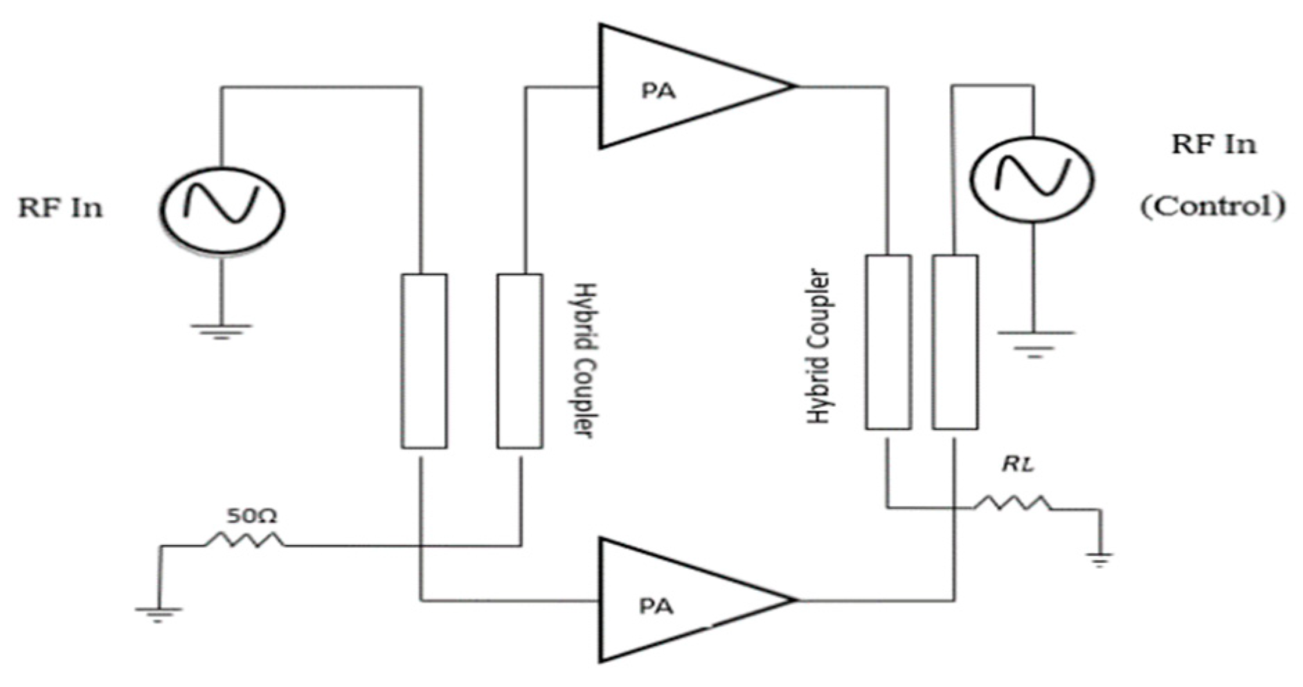
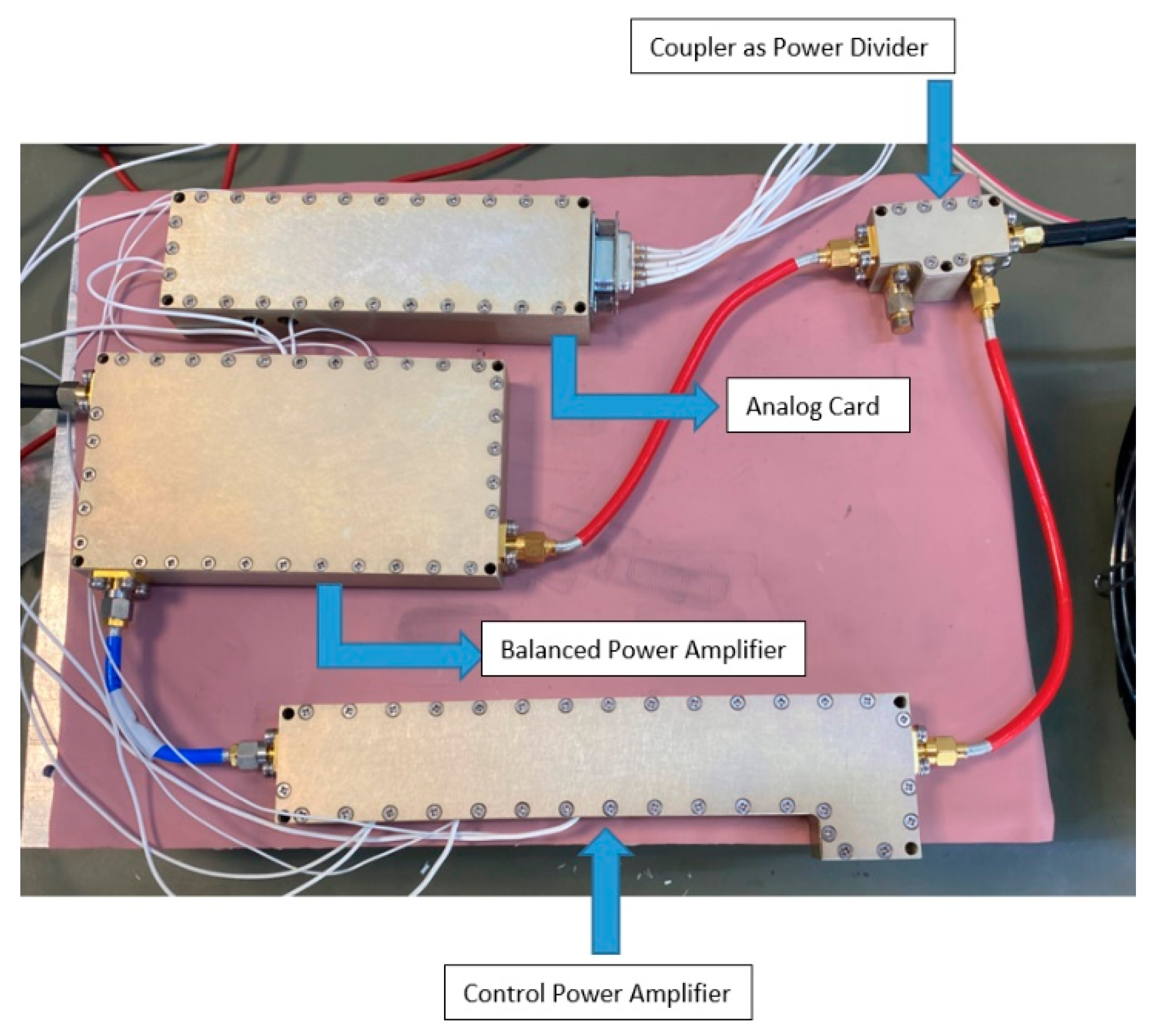
2.1. Load-Modulated Balanced Amplifier Design

AWR software packages (AWR V14) were used for LMBA electronic hardware design, and the Solidworks (Solidworks 2018) software package was used for mechanical design. The control path power amplifier, main path (balanced pair) power amplifier, and directional coupler used as a power splitter were designed as subsystems of the designed LMBA architecture. In the design of these subsystems, instead of the standard FR4 base material, Rogers’ RO4003C base material designed for high frequencies was used. The advantages of RO4003C base material over FR4 base material are that it has less loss, can operate at higher operating temperatures, and provides a constant dielectric constant.

2.2. Control Path Power Amplifier Design

The purpose of the control path is to increase the load impedance of the main path when the output power is low so that it can operate with higher efficiency. If the control path is of high saturation power, the load impedance of the main path may change too much, and the efficiency gain may decrease. For this reason, the control path is usually chosen to have less saturation power than the main path. If the control path is of high power, it may create an aggressive effect during load modulation, which may adversely affect the linearity performance of the system.
As a result, selecting a control path power lower than the main path increases efficiency, makes load modulation more stable, and improves linearity performance. The same consideration can be found in [15,21].
To achieve active load modulation successfully, the transistors in the control path must saturate earlier than the transistors in the main path. For this purpose, the output power of the transistor used in the control path must be selected to be lower than the transistors to be used in the main path. In the market research, in order to best meet the requirements of this study, Macom’s CG2H40010F transistor (Lowell, MA, USA) with 10 W output power was used for the control path and CG2H40025F with 25 W output power was used for the transistors in the main path.
A minimum output power of 10 W was targeted in the control path. JSPHS-23+ phase shifter integration of Mini-Circuits was used to provide a phase change in the control path. In the simulation studies for the design, nonlinear models of transistors provided by Macom were used. In order for the power amplifier to operate as Class-B, there must be no quiescent current. For this, −2.8 V was applied as the gate voltage.
After determining the gate voltage, load-pull analysis was performed. The purpose of the load-pull analysis was to determine the output power and efficiency parameters resulting from the change in the impedance value seen by the transistor. In this way, the most suitable impedance for the design can be determined. Load-pull analysis was performed for 1800 MHz, which is the center frequency of the design.
When designing the input matching network, care was taken to ensure that the maximum power could be delivered to the transistor and that the system was absolutely stable. Rollet Stability (K) and B1 auxiliary stability factors were examined in stability analyses. Here, the main goal was the stable operation of the transistor. For this, K > 1, B1 > 0 conditions must be met [22]. By paying attention to the above criteria, a fine-tuned input matching network was designed.
After the input matching network design was completed, the output matching network of the transistor was designed. Load-pull analysis was utilized in the design. The output power and efficiency contours of the transistor were plotted as a result of the load-pull analysis. Figure 3 shows the results of the load-pull analysis. Here, as seen in the Smith Chart, pink contours represent the PAE and blue contours represent the output power. The blue contours represent impedance values where the output power increases with decreasing impedance values and the pink contours represent impedance values where the PAE increases with decreasing impedance values. The normalized impedance value was chosen to maximize the output power, and the matching network was constructed accordingly.
According to these results, the best-normalized output impedance was determined as 0.375 + i 0.26, and the design was made in accordance with this impedance value. The output matching network of the power amplifier planned to be used in the control path was designed by paying attention to parameters such as stability, output power, and efficiency.
When the results obtained are analyzed, it is seen that the control path will have an average gain of 14 dB at an output power of 40–41 dBm; in other words, a signal with a power of 26–27 dBm will need to be applied from the input. When the manufacturer data of the JSPHS23+ Phase Shifter are examined, it is seen that the maximum input power is 20 dBm. Since the JSPHS23+ Phase Shifter cannot be used just before the power amplifier design, we decided to use two lower-output power amplifiers between the phase shifter and the power amplifier design. In this context, we determined that it would be appropriate to use the GVA-123+ and PHA-102+ products of Mini-Circuits. The control path power amplifier design was completed by adding S parameter files of these amplifiers in the design.
After the design was completed, the control path power amplifier was also manufactured. The fabricated control path power amplifier is given in Figure 4.
After the production was completed, efficiency and gain values were measured separately at 1700, 1800, and 1900 MHz by using an RF signal generator (Rohde & Schwarz (Munich, Germany) SMC100A), a DC power supply and a power meter (Rohde & Schwarz (Munich, Germany) NRP18P), in the laboratory environment. The measurements made in the real environment using the manufactured board were compared with the simulation results in the design environment. The output power and drain efficiency graphs obtained in this context are given in Figure 5 and Figure 6. As can be seen in Figure 6 and Figure 7, the design and production results for the efficiency values of the control path power amplifier are close to each other.
After comparing the efficiency results, the simulation and measurement results of the control path power amplifier output power and gain results were compared. The output power/gain graphs of the control path power amplifier are given in Figure 7 and Figure 8. The control path power amplifier gains show a difference of approximately 0.5–1 dB between the design and measured results. This difference is attributed to the discrete elements in the RF path and the printed circuit board.

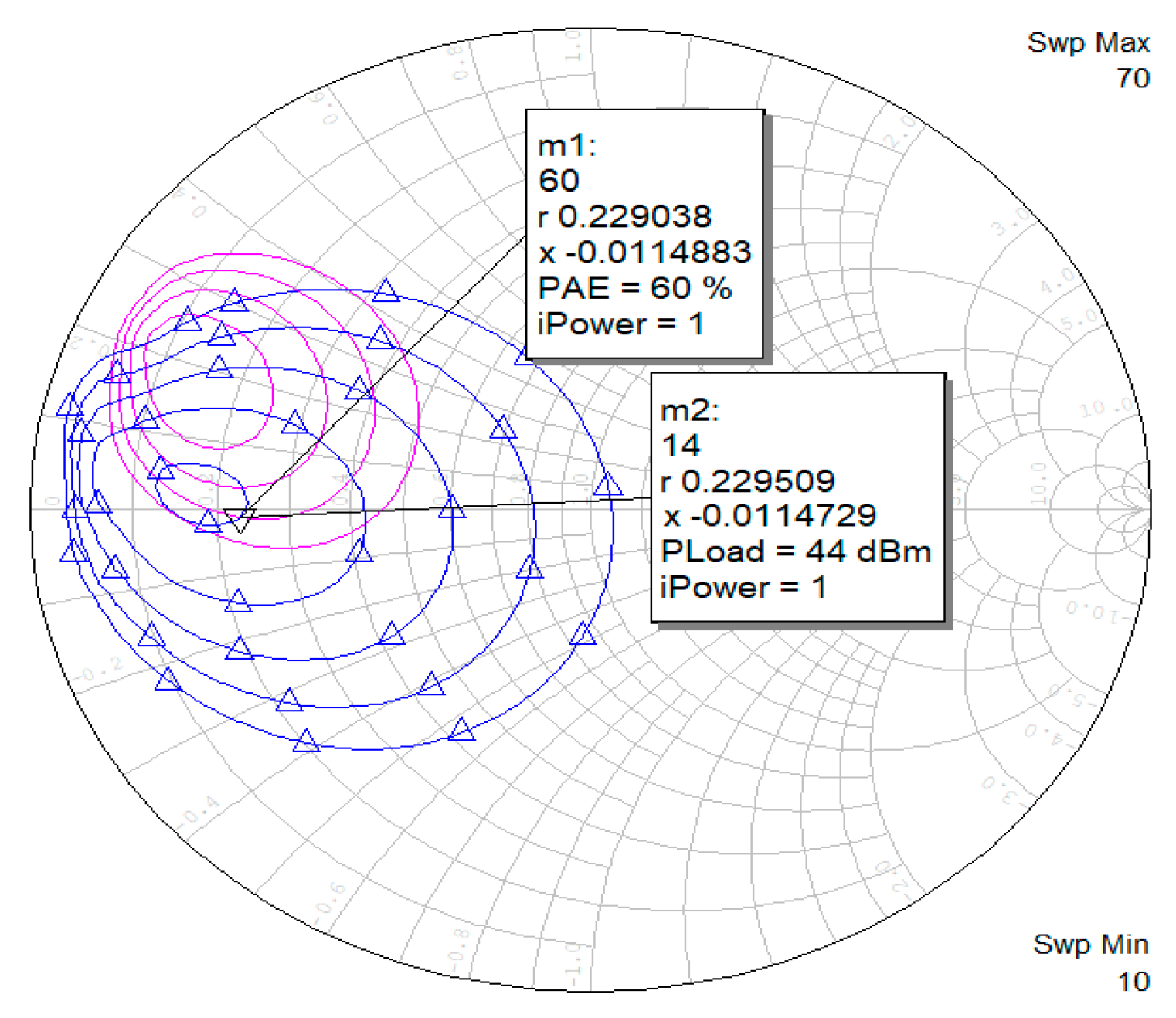
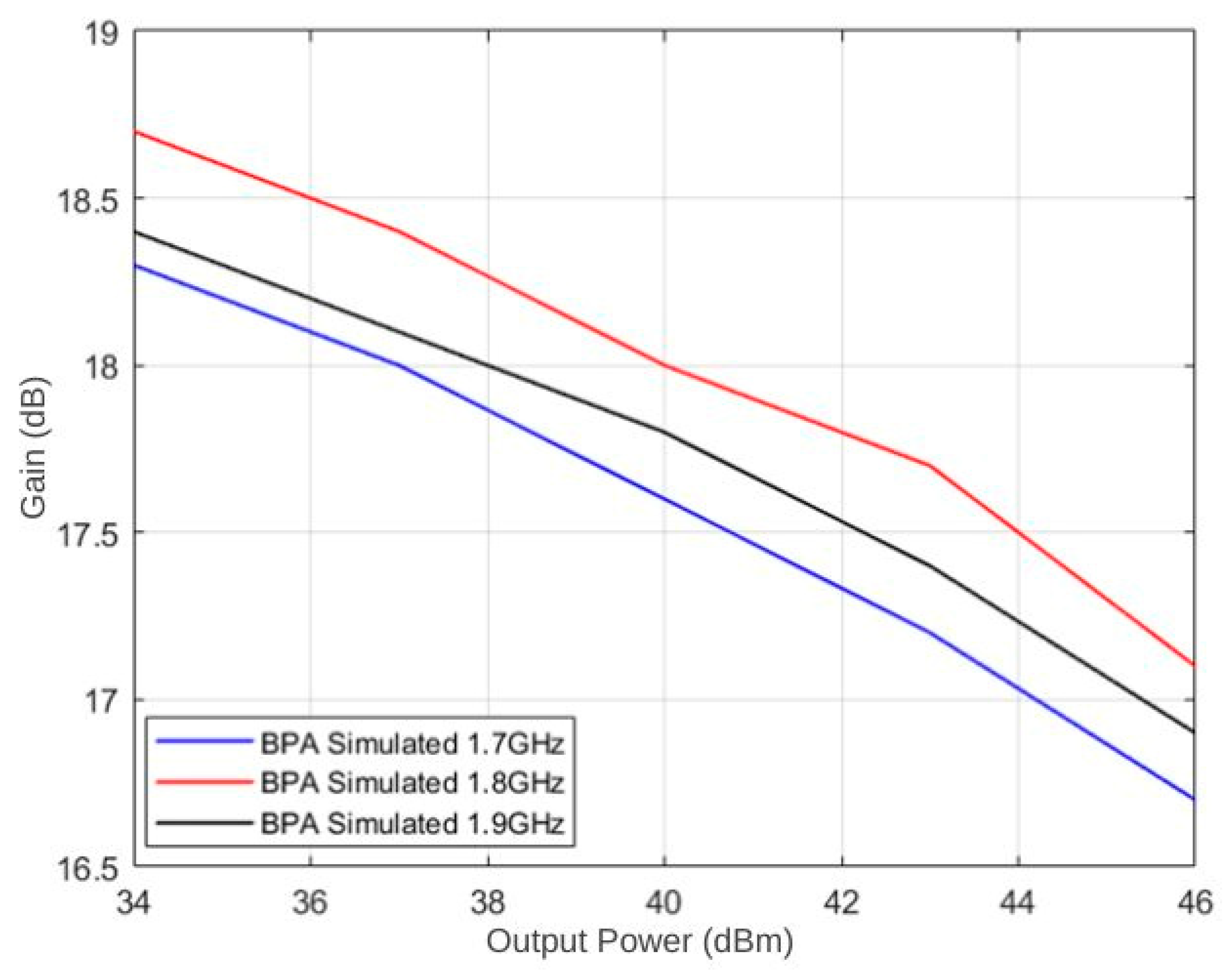
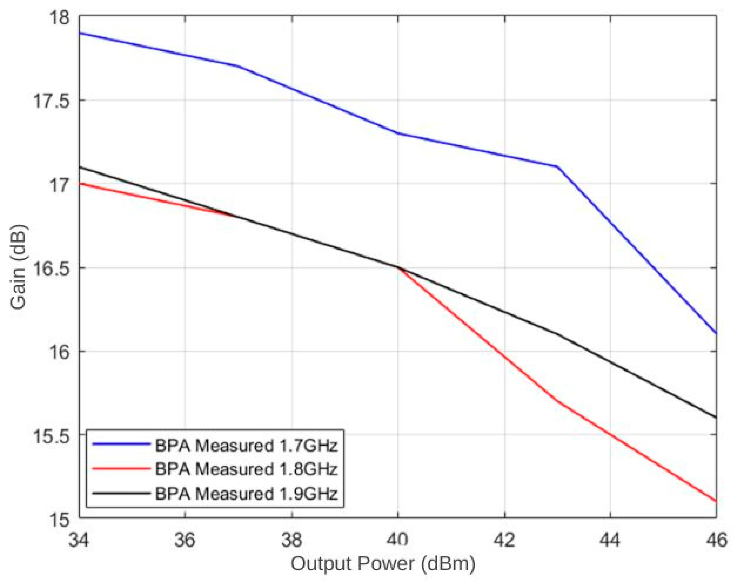
2.3. Balanced Pair (Main Path) Power Amplifier Design

In the design of the balanced pair, CG2H40025F transistors from MACOM (Lowell, MA, USA) were used as power transistors, and IPP-7032 from Innovative Power Products (Holbrook, NY, USA) was used as a hybrid coupler. A minimum output power of 40 W was targeted as the target power in the main path.
Class-AB operation was achieved by adjusting the gate voltage of the selected transistor. For this, the quiescent current was set to 250 mA, as recommended by the manufacturer. Simulation studies in the design were carried out by using the nonlinear model of the transistors provided by Macom (Lowell, MA, USA).
Load-pull analysis was performed for 1800 MHz, which is the center frequency of the design. The purpose of the load-pull analysis was to determine the output power and efficiency parameters as a result of the change in the impedance value seen by the transistor. In this way, the most suitable impedance for the design was determined.
When designing the input matching network, as in the design of the control path power amplifier, care was taken to ensure that maximum power could be delivered to the transistor and that it was absolutely stable. In the stability analysis, Rollet Stability (K) and B1 auxiliary stability factor values were analyzed. For the stable operation of the transistor, K > 1 and B1 > 0 conditions were aimed to be met [22].
According to the above criteria, the input matching network was designed by fine-tuning. After the input matching network design was completed, the output matching network of the transistor was designed. Load-pull analysis was used in the design. The output power and efficiency contours of the transistor were plotted as a result of the load-pull analysis. Figure 9 shows the results of the load-pull analysis. Here, the pink contours in the Smith Chart represent the PAE and the blue contours represent the output power. The blue contours represent the impedance values where the output power increases with decreasing impedance values and the pink contours represent the impedance values where the PAE increases with decreasing impedance values. The normalized impedance value was chosen to maximize the output power, and the matching network was constructed accordingly.
According to these results, the most appropriate normalized output impedance was determined as 0.229 − i 0.011, and the design was made in accordance with this impedance value. The output matching network of the power amplifier planned to be used in the control path was designed by paying attention to parameters such as stability, output power, and efficiency.
The load-pull analysis for the balanced amplifier path was performed for a single transistor. This structure was made suitable for the balanced amplifier topology by using the IPP-7032 hybrid coupler from Innovative Power Products (Holbrook, NY, USA).
The design of the balanced power amplifier was completed, and the production of the balanced pair power amplifier was also realized. The produced balanced pair power amplifier is given in Figure 10. After the production was completed, efficiency and gain values were measured separately at 1700, 1800, and 1900 MHz in the laboratory environment. The measurements made in the real environment using the manufactured board were compared with the simulation results in the design environment. The output power and drain efficiency graphs of the balanced pair power amplifier obtained in this context are given in Figure 11 and Figure 12. When the results are analyzed, it is seen that the simulation results and measurement results are close to each other.
After the balanced pair efficiency results were analyzed, the gain results were compared. The output power/gain graphs of the balanced pair power amplifier are given in Figure 13 and Figure 14. The results indicate that there is a 1–1.5 dB gain difference between the simulation results and the measurement results. This difference may be due to discrete elements in the RF path and the printed circuit board. This completes the design and stand-alone measurements of the balanced pair.

2.4. Directional Coupler Design to Be Used as a Power Splitter

As a result of the simulations, it is seen that there will be a difference of approximately 30 dBm between the input power of the control path and the input power of the balanced pair. Due to this large difference, instead of designing two equal power splitters, it is preferred to design a directional coupler with a minimum coupling of 15 dB and use an unequal power splitter.
The obtained simulation and measurement results of the insertion loss, return loss, and coupling factor show that there is about a 1 dB difference in the coupling factor between the simulation and measurement results. Since the aim here is to create an average difference of 15 dB between the input power of the control path and the balanced pair, the 1 dB difference is not significant. For the return loss, a design to achieve a minimum of 20 dB is sufficient.

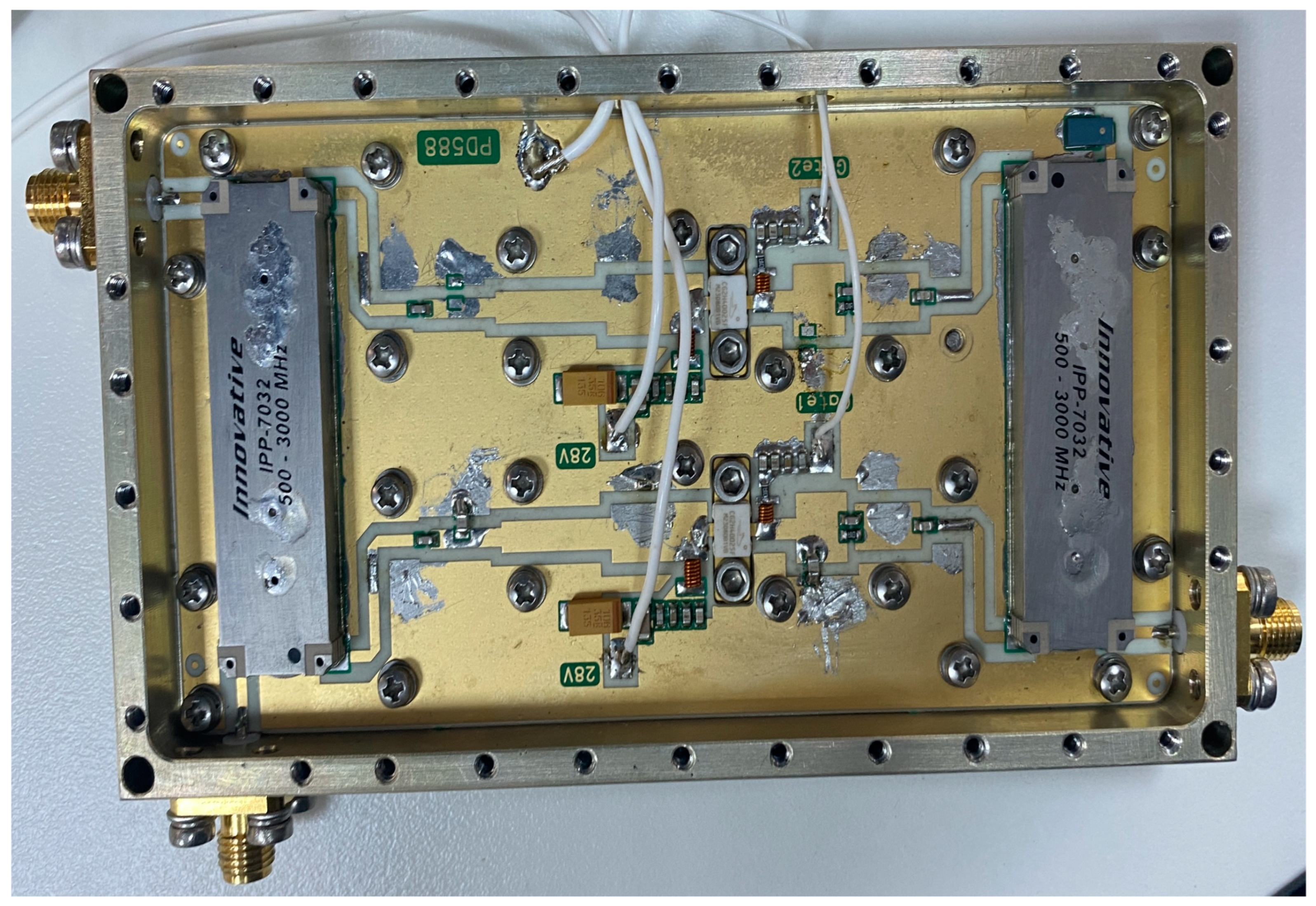
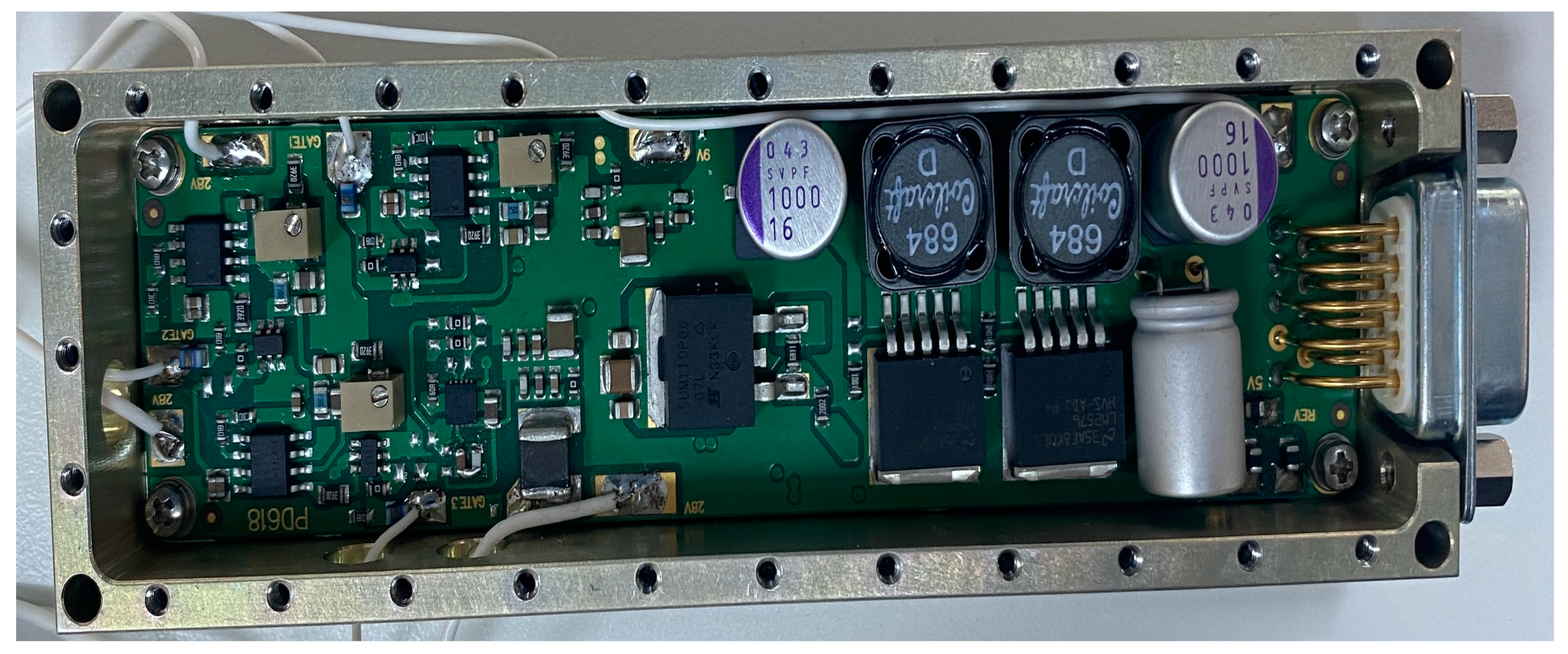
2.5. Analog Board Design

In the designed Single RF-Input LMBA structure, 5 V, 9 V, −5 V, and 28 V are required. Here, 28 V is needed for the drain voltages of the transistors, −5 V is needed to adjust the gate voltages of the transistors with the voltage divider structure, and 5 V and 9 V are needed to use the GVA123+ and PHA102+ units, respectively. An analog board was designed to provide these voltages from a single power supply. In this way, all gate voltages and drain voltages were obtained by using a single power supply. The analog board that meets the specified requirements is given in Figure 15.

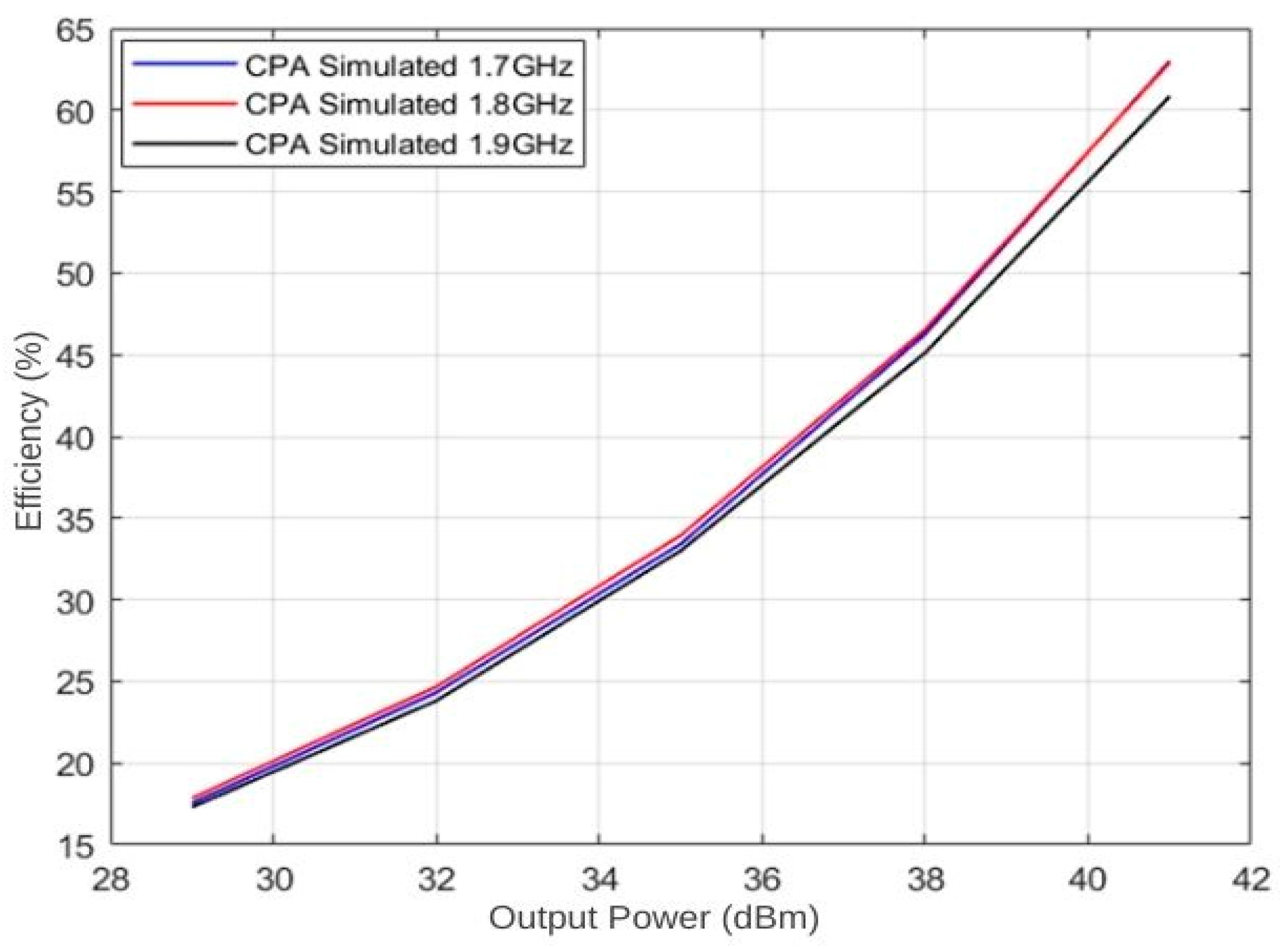
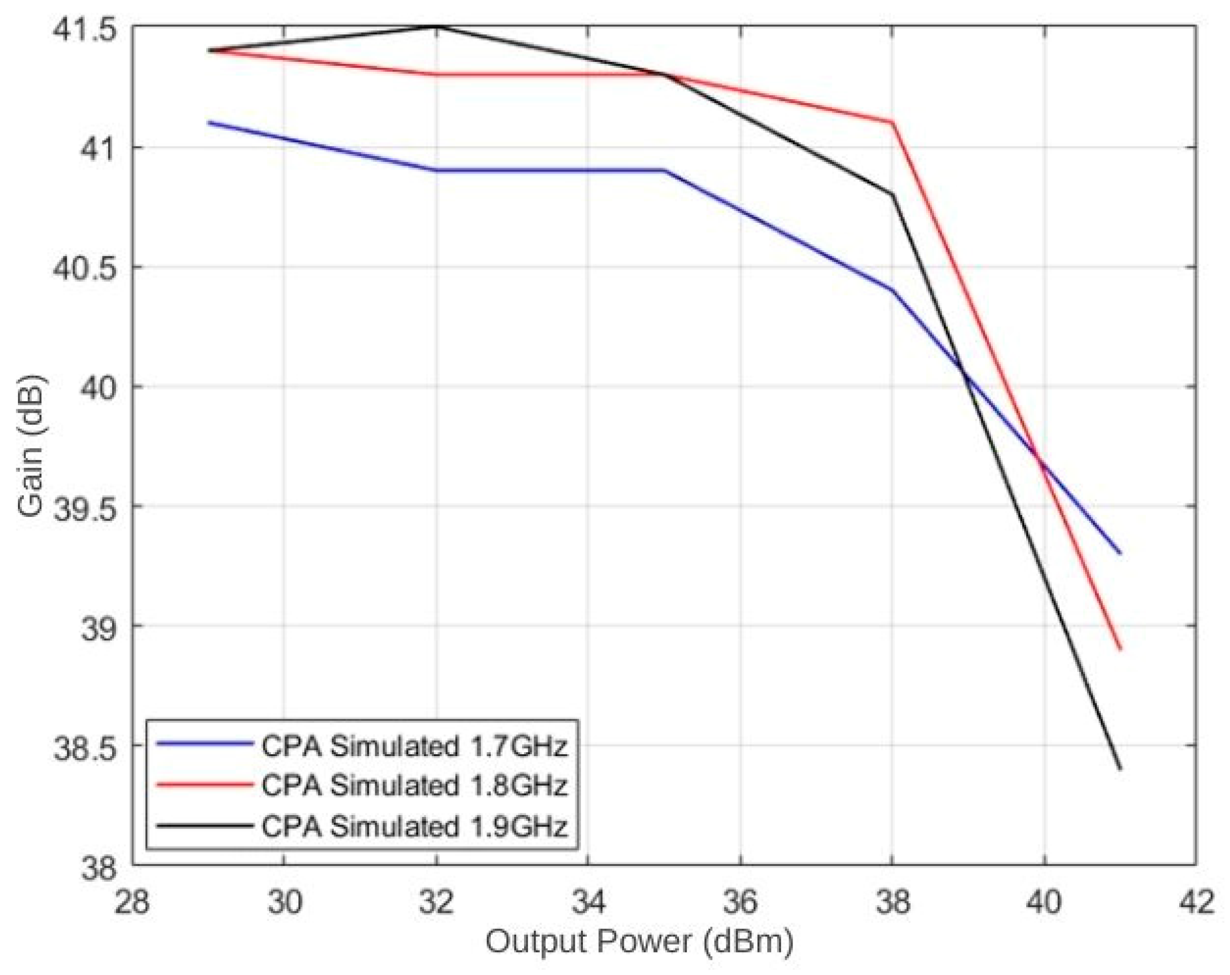
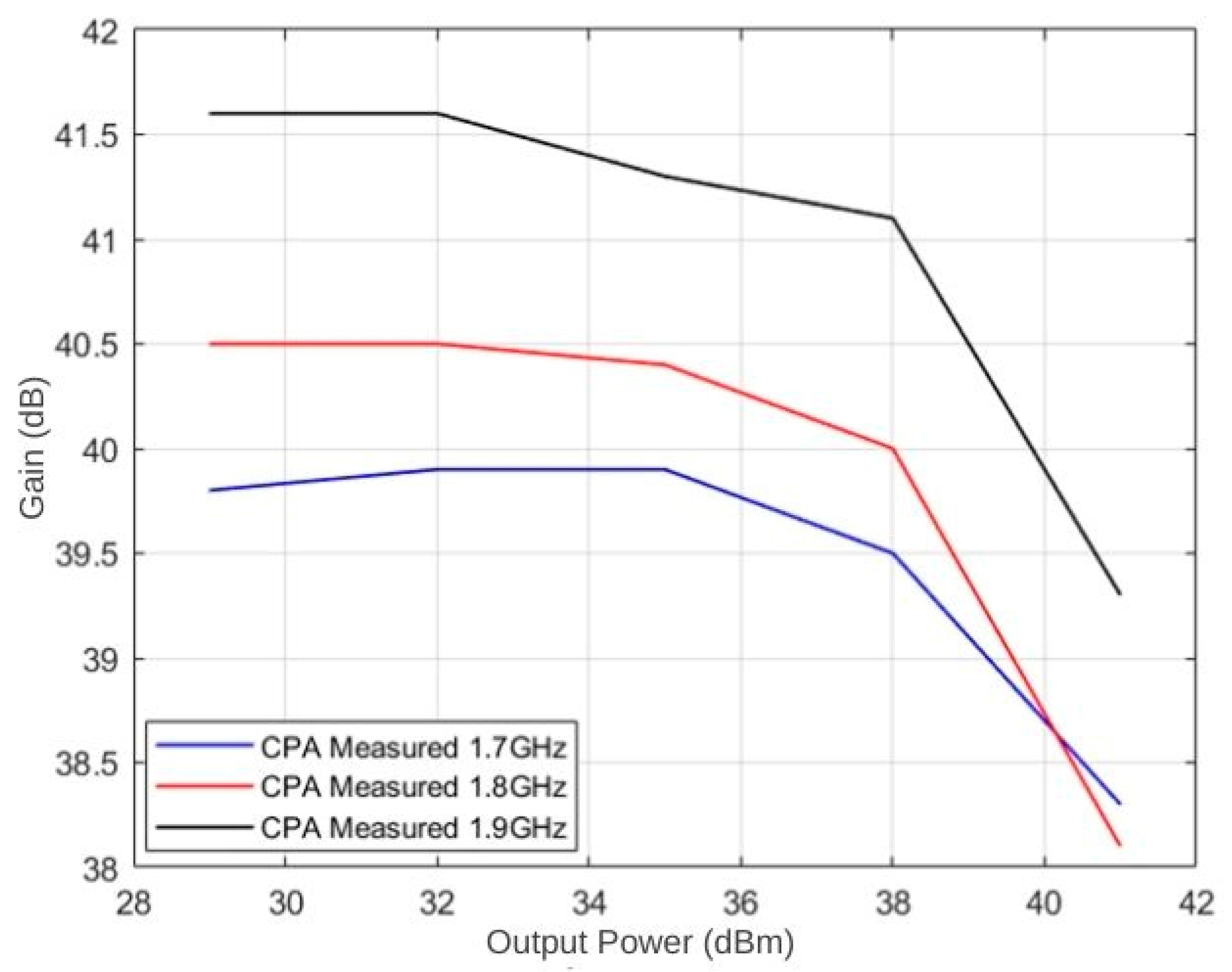
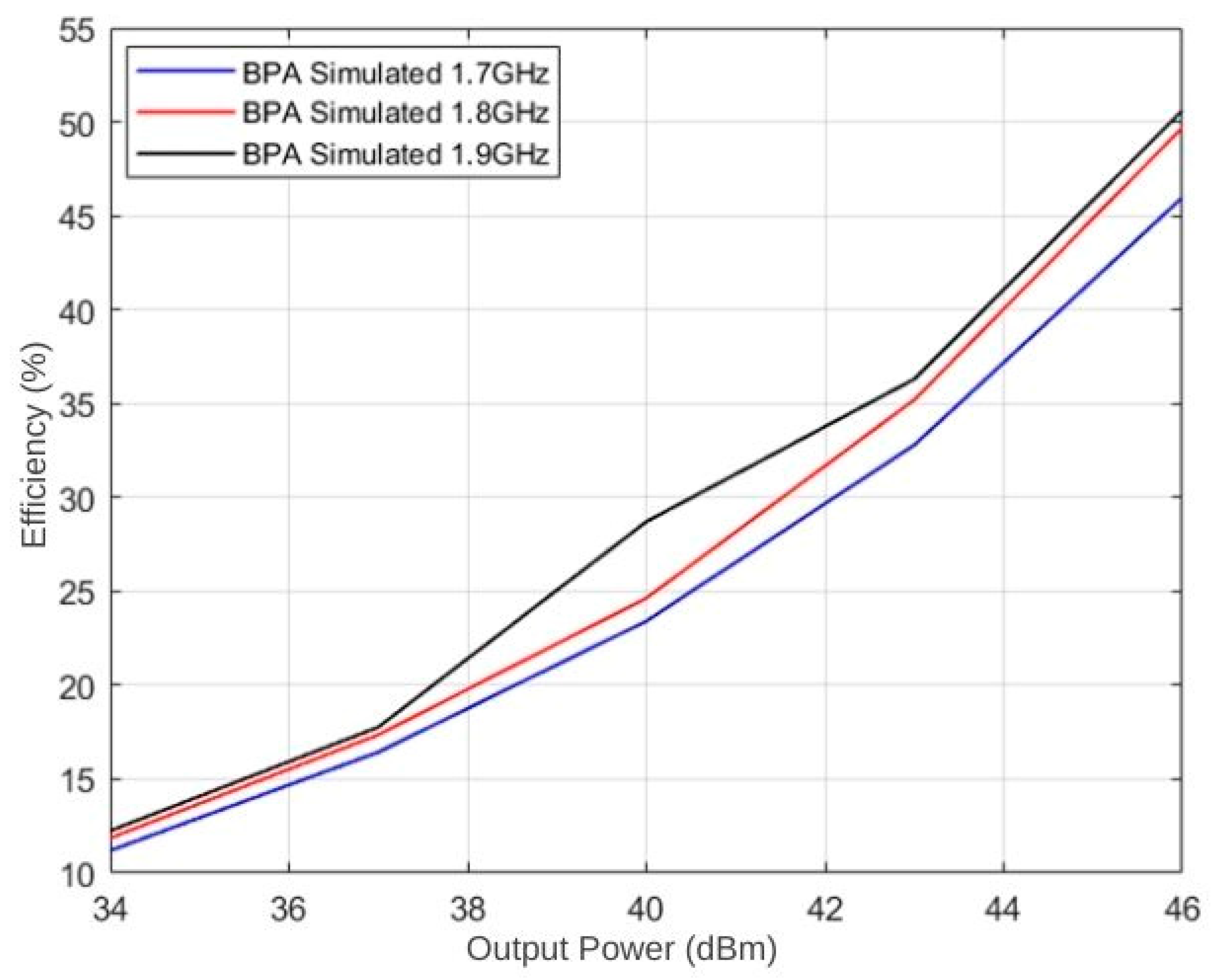
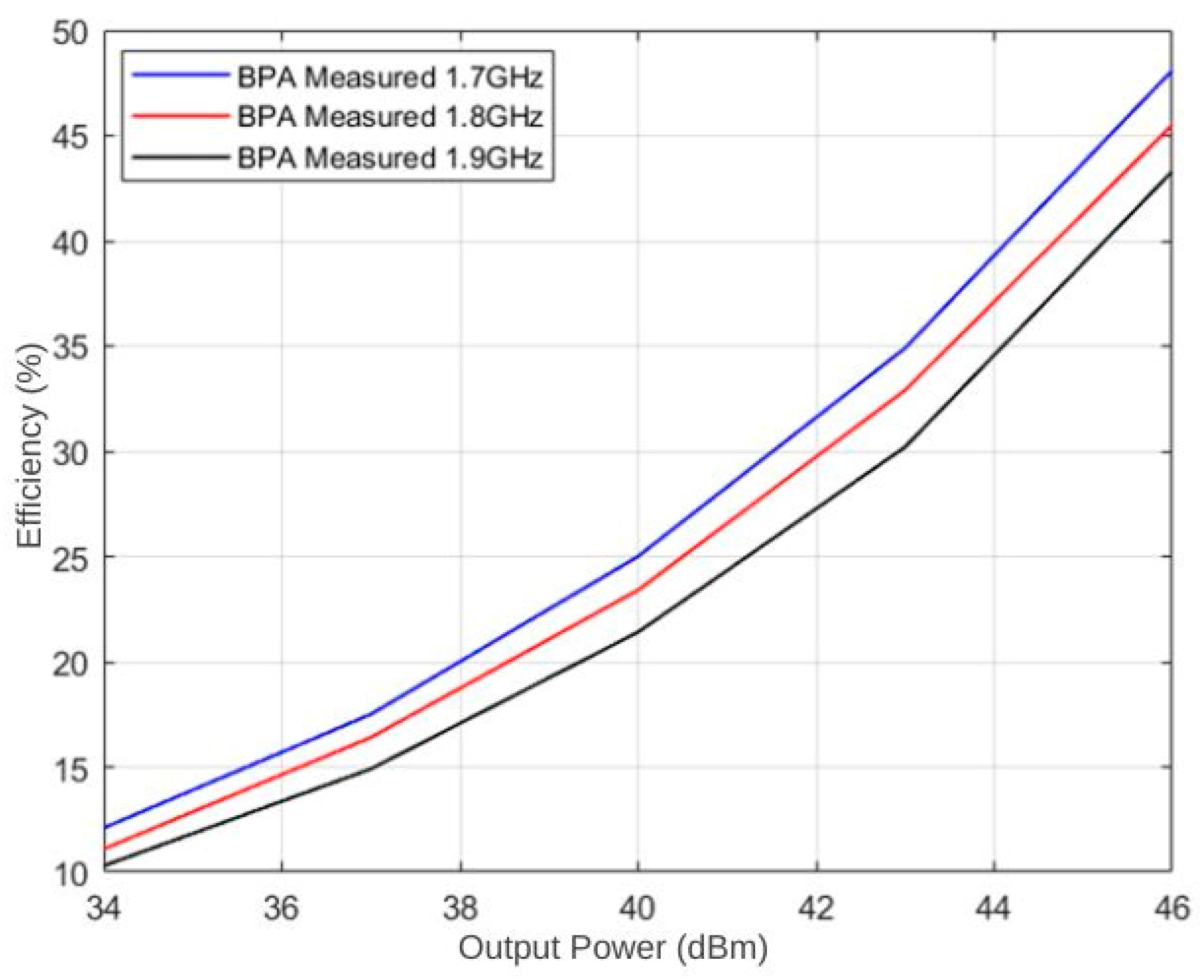
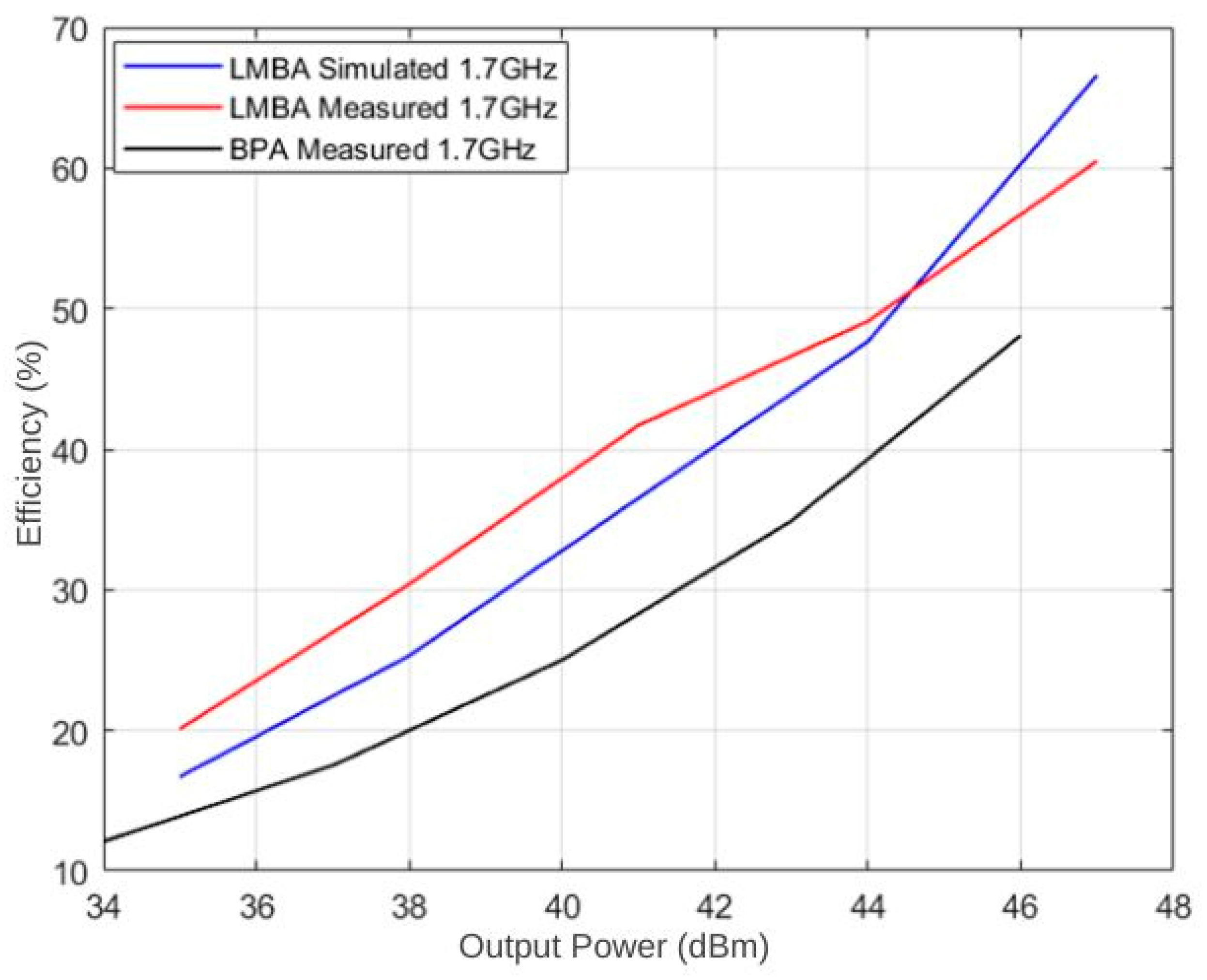
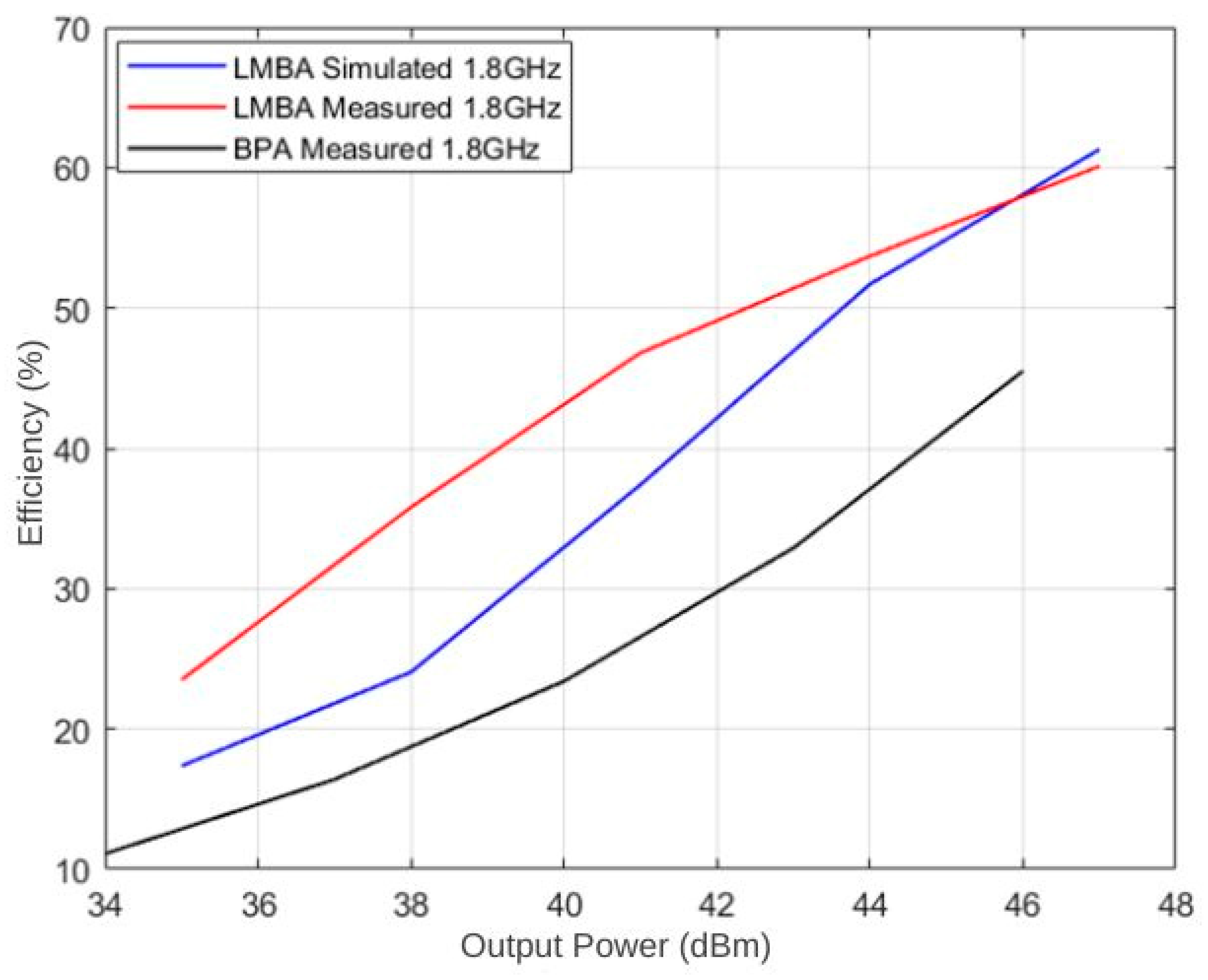
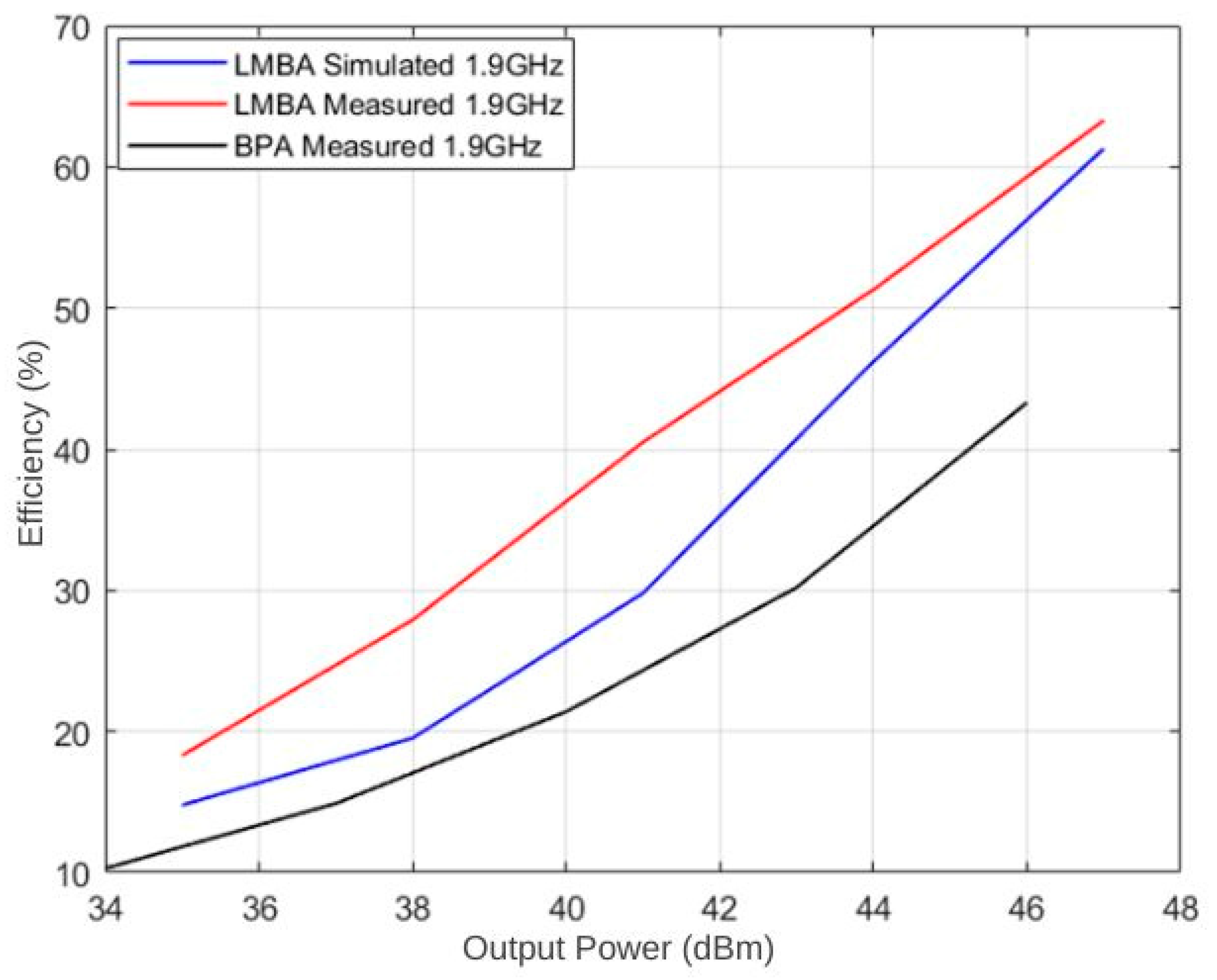
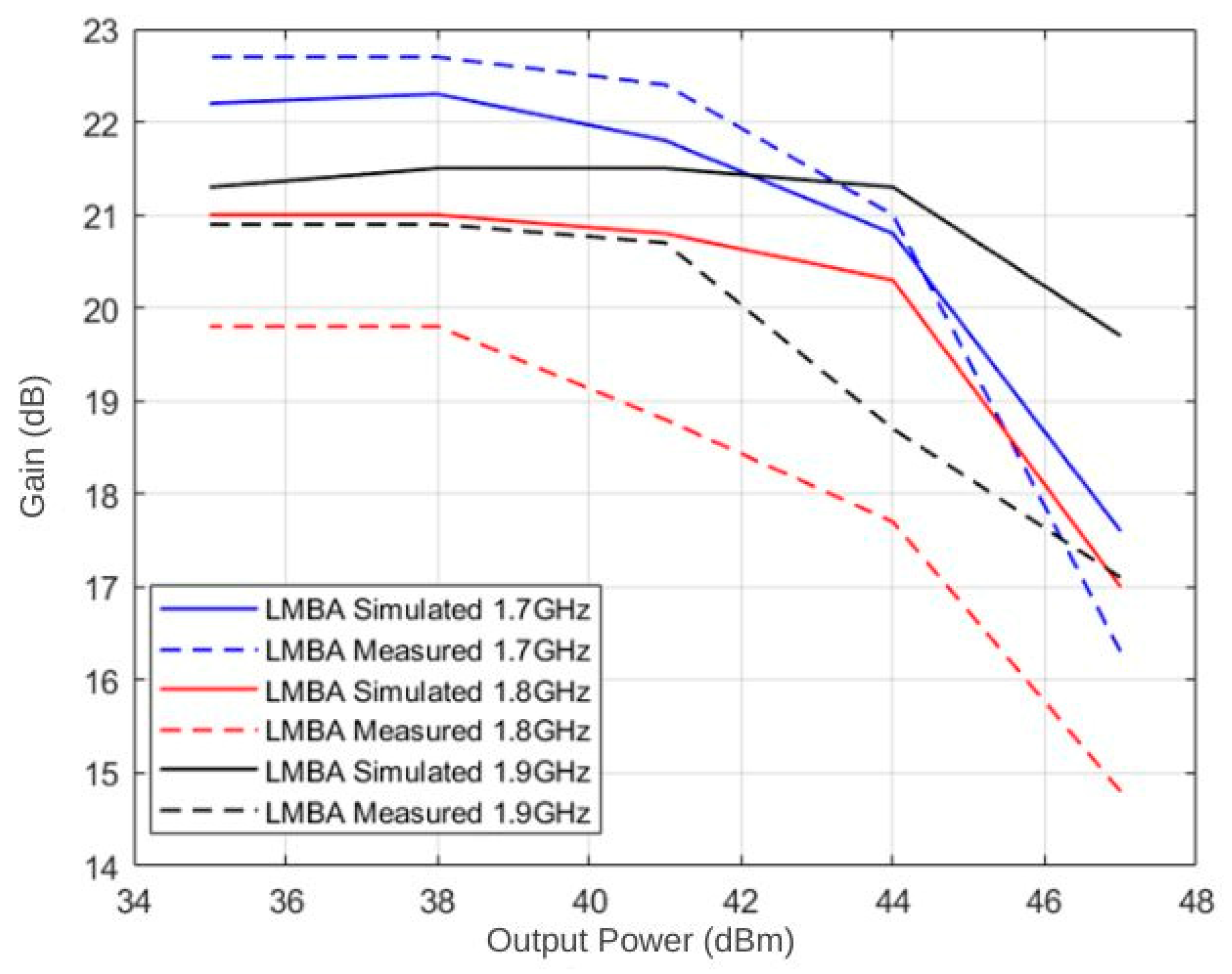
3. Measurement Results of the LMBA System

Using the control path power amplifier, balanced pair power amplifier, and the directional coupler used as a power splitter and analog board, which were all explained in detail in the previous section, the LMBA, which we aimed to design and manufacture within the scope of this article, was realized as a prototype. The realized LMBA is shown in Figure 16.
As explained in detail in the previous section, the structures used in the LMBA system were measured alone, and the desired results were obtained. When the results are analyzed, it is seen that when the balanced amplifier is measured alone, it operates with a drain efficiency of 43–48% at 46 dBm output power and with a drain efficiency of 21–25% at 6 dB output back-off.
A simulation of the LMBA in the fabricated prototype system was performed. The simulation results, measurement results, and efficiency results of the balanced pair without the LMBA structure were compared. When the graphs in Figure 17, Figure 18 and Figure 19 are examined, it is seen that the efficiency results of the LMBA structure are better than the balanced amplifier efficiency results at all output powers. Another point to be emphasized here is that the efficiency measurement results of the LMBA system produced are better than the efficiency simulation results for the LMBA system at every frequency.
Another important issue is to examine the gain values of the LMBA produced. In this context, the gain and output power of the load-modulated balanced amplifier, which was designed and prototyped, were analyzed at several frequencies. The fabricated LMBA prototype and simulation results were compared in terms of output power and gain. The results obtained are shown in Figure 20. When the LMBA output power and gain results are analyzed, it is seen that there is a 1.5–2 dB gain difference between the simulation and measurement results.

4. Discussion

In the following paragraphs, the results obtained so far will be summarized and the LMBA and balanced amplifier measurement results will be compared. The designed and prototyped LMBA was first compared with a conventionally designed balanced amplifier without load modulation. Table 1 summarizes the balanced amplifier measurement results. Table 2 summarizes the measurement results of the designed and prototyped LMBA. By comparing Table 1 with Table 2, it was determined that the output power increased by 10 W with the LMBA configuration. At the maximum output power level, the drain efficiency increased by 12.4–20% in the frequency range of 1700–1900 MHz and by 16.7–23.4% at 6 dB output back-off in the same frequency range. It was observed that the results obtained are also close to the simulation results.
The calibration was performed at 25 °C for each frequency and power level of the system. The phase delays of the coaxial cables used in the transitions between subsystems were also taken into account in this context.
At this stage, the LMBA system was produced in a modular form to allow individual testing of the subsystems. To increase the usability of the system, the LMBA system can also be constructed within a single mechanical structure using a single substrate.
Concerning the management of the control signal, the input signal power of the system was adjusted for maximum output power, 3 dB low output power, and 6 dB low output power for each frequency, and the phase of the control arm was changed by changing the control voltage (the load impedance of the transistors in the main arm was changed). Frequency/input power/output power/control voltage value information is stored in a Look-Up-Table for Adaptive Load Modulation.
In our study, the measurement results of the balanced amplifier topology and the Single RF-Input LMBA architecture were obtained by adding a control signal to the balanced topology (this control signal was obtained by generating the control signal from the input signal, not from outside). The measurement results of these two architectures were compared.
Another important issue is to make comparisons with other studies in the literature similar to our study in this article. For this purpose, the LMBA, which was produced as a prototype within the scope of this article, and some other studies in the literature are compared in Table 3. In the comparison, it is seen that the LMBA power amplifier designed and manufactured within the scope of this article achieves higher output power compared to other similar studies in the literature.

5. Conclusions

In this paper, a Single RF-Input load-modulated balanced amplifier was designed and fabricated. The amplifier was tested and measured by using calibrated RF measurement devices at RFTR Elektronik (Ankara, Türkiye) A.Ş. facilities. The measurements showed that 47 dBm (50 W) output power, 60.1–63.3% drain efficiency at maximum output power, and 40.5–46.8% drain efficiency at 6 dB output back-off were achieved in the frequency range of 1.7 GHz–1.9 GHz. The LMBA measurement results were compared with conventionally designed balanced amplifiers without load modulation. With the LMBA configuration, it was determined that the efficiency increased by 12.4–20% at maximum output power and by 16.7–23.4% at 6 dB output back-off in the same frequency range.
Noise performance is an important factor for an amplifier. In our LMBA study, our main focus was to increase the efficiency both at maximum power and at low output power. We wanted to show that we could achieve this without reducing the system gain. We consider the importance of noise performance measurement as an important issue. Therefore, we strongly recommend that it be taken into account in detail in a further study. Furthermore, as a follow-up study, we proposed to design and compare LMBAs with a similar output power level and octave bandwidth.

Author Contributions

Conceptualization, M.Ü. and E.M.; methodology, M.Ü.; software, E.M.; validation, E.M.; formal analysis, M.Ü. and E.M.; investigation, M.Ü. and E.M.; resources, M.Ü. and E.M.; data curation, E.M.; writing—original draft preparation, M.Ü.; writing—review and editing, M.Ü.; visualization, E.M.; supervision, M.Ü. All authors have read and agreed to the published version of the manuscript.

Funding

This research received no external funding.

Data Availability Statement

Data are contained within the article.

Acknowledgments

We would like to thank Necip ŞAHAN, General Manager of RFTR Elektronik A.Ş. and Vahdettin T.A.Ş., Design and Engineering Director, for allowing us to use the technical infrastructure of the company at every stage of the design and production of the Load Modulation Balanced Amplifier in this article.

Conflicts of Interest

The authors declare no conflicts of interest.

References

  1. Bayraktar, F. Yüksek Verimli F-Sınıfı Mikrodalga Güç Yükselteç Tasarımı. Master’s Thesis, Elektrik Elektronik Mühendisliği, Hacettepe Üniversitesi, Ankara, Türkiye, 2017. [Google Scholar]
  2. Skaria, G. Class F and Inverse Class F Power Amplifier Subject to Electrical Stress Effect. Master’s Thesis, Department of Electrical Engineering and Computer Science, University of Central Florida, Orlando, FL, USA, 2011. [Google Scholar]
  3. El-Hamamsy, S.A. Design of high-efficiency RF Class-D power amplifier. IEEE Trans. Power Electron. 1997, 9, 297–308. [Google Scholar] [CrossRef]
  4. Collins, G.F.; Wood, J. Class-E power amplifier design at 2.5 GHz using a packaged transistor. In Proceedings of the 2013 IEEE Radio and Wireless Symposium, Austin, TX, USA, 20–23 January 2013; pp. 259–261. [Google Scholar] [CrossRef]
  5. Kahn, L.R. Single-Sideband Transmission by Envelope Elimination and Restoration. Proc. IRE 1952, 40, 803–806. [Google Scholar] [CrossRef]
  6. Jing, Y.; Zhu, B. A 2.4 GHz SiGe Envelope Tracking Power Amplifier for LTE Applications. In Proceedings of the 2023 6th World Conference on Computing and Communication Technologies (WCCCT), Chengdu, China, 6–8 January 2023; pp. 52–56. [Google Scholar] [CrossRef]
  7. Peker, K. Design of a High Efficiency Power Amplifier by Using Doherty Configuration. Master’s Thesis, Department of Electrical and Electronics Engineering, Bilkent University, Ankara, Turkey, 2010. [Google Scholar]
  8. Zeng, B.; Zheng, S.; Chan, W.S.; Zhou, X. Design of a High-Efficiency Outphasing Power Amplifier with Enhancing Back-Off Range for 5G Applications. In Proceedings of the 2023 IEEE Conference on Antenna Measurements and Applications (CAMA), Genoa, Italy, 15–17 November 2023; pp. 442–444. [Google Scholar] [CrossRef]
  9. Yang, K.; Yang, R.; Zhang, P.; Shi, W.; Hu, C.; Shi, W. Development Review of Highly Efficient Sequential Power Amplifier with Extended Back-Off Range for Broadband Application. Energies 2024, 17, 161. [Google Scholar] [CrossRef]
  10. Jin, D.; Latino, M.; Crupi, G.; Cai, J. Design and Experimental Validation of a High-Efficiency Sequential Load Modulated Balanced Amplifier. Electronics 2024, 13, 3897. [Google Scholar] [CrossRef]
  11. Jin, Y.; Dai, Z.; Ran, X.; Xu, C.; Li, M. A Dual Load-Modulated Doherty Power Amplifier Design Method for Improving Power Back-Off Efficiency. Sensors 2023, 23, 6598. [Google Scholar] [CrossRef] [PubMed]
  12. Niclas, K.B.; Wilser, W.T.; Gold, R.B.; Hitchens, W.R. Application of the Two-Way Balanced Amplifier Concept to Wide-Band Power Amplification Using GaAs MESFET’s. IEEE Trans. Microw. Theory Tech. 1980, 28, 172–179. [Google Scholar] [CrossRef]
  13. Quaglia, R.; Cripps, S. A Load Modulated Balanced Amplifier for Telecom Applications. IEEE Trans. Microw. Theory Tech. 2018, 66, 1328–1338. [Google Scholar] [CrossRef]
  14. Pednekar, P.H.; Barton, T.W. RF-input load modulated balanced amplifier. In Proceedings of the 2017 IEEE MTT-S International Microwave Symposium (IMS), Honololu, HI, USA, 4–9 June 2017; pp. 1730–1733. [Google Scholar] [CrossRef]
  15. Pednekar, P.H.; Berry, E.; Barton, T.W. RF-Input Load Modulated Balanced Amplifier with Octave Bandwidth. IEEE Trans. Microw. Theory Tech. 2017, 65, 5181–5191. [Google Scholar] [CrossRef]
  16. Pednekar, P.H.; Hallberg, W.; Fager, C.; Barton, T.W. Analysis and Design of a Doherty-Like RF-Input Load Modulated Balanced Amplifier. IEEE Trans. Microw. Theory Tech. 2018, 66, 5322–5335. [Google Scholar] [CrossRef]
  17. Cao, Y.; Lyu, H.; Chen, K. Load Modulated Balanced Amplifier with Reconfigurable Phase Control for Extended Dynamic Range. In Proceedings of the 2019 IEEE MTT-S International Microwave Symposium (IMS), Boston, MA, USA, 2–7 June 2019; pp. 1335–1338. [Google Scholar] [CrossRef]
  18. Aras, Y.E. Analytical Model and Design of Load Modulated Balanced Amplifier. Master’s Thesis, The Graduate School of Engineering and Science, Bilkent University, Ankara, Turkey, 2020. [Google Scholar]
  19. Xie, J.; Cheng, K.-K.M.; Fang, X.; Yu, P. Extension of Output Backoff Range in Three-Stage Load Modulated Balanced Amplifier Using Asymmetric Coupling and Non-Z0 Load. IEEE Trans. Microw. Theory Tech. 2025, 73, 553–567. [Google Scholar] [CrossRef]
  20. Ding, L.; Xia, J. Design of Load-modulated Balanced Amplifier Based on Broadand Output Matching Network. In Proceedings of the 2024 IEEE 12th Asia-Pacific Conference on Antennas and Propagation (APCAP), Nanjing, China, 22–25 September 2024; pp. 1–2. [Google Scholar] [CrossRef]
  21. Pednekar, P.H. Advanced Load Modulated Power Amplifier Architectures. Doctoral Thesis, Faculty of the Graduate School, University of Colorado at Boulder, Boulder, CO, USA, 2019. [Google Scholar]
  22. Mehter, E.; Bilgiç, R.; Üçüncü, M. Radar HF Bandı RF Güç Yükselteci Tasarımı ve Üretimi. Bitlis Eren Üniv. Fen Bilim. Derg. 2021, 10, 1232–1248. [Google Scholar] [CrossRef]
Figure 1. LMBA architecture block diagram.
Electronics 14 01435 g001
Figure 2. Single RF-Input LMBA block diagram [13].
Electronics 14 01435 g002
Figure 3. Control path power amplifier load-pull analysis.
Electronics 14 01435 g003
Figure 4. Control path power amplifier.
Electronics 14 01435 g004
Figure 5. Control path power amplifier efficiency simulation results.
Electronics 14 01435 g005
Figure 6. Control path power amplifier efficiency measurement result.
Electronics 14 01435 g006
Figure 7. Control path power amplifier gain simulation.
Electronics 14 01435 g007
Figure 8. Control path power amplifier gain measurement.
Electronics 14 01435 g008
Figure 9. Balanced pair power amplifier load-pull analysis.
Electronics 14 01435 g009
Figure 10. Balanced pair power amplifier.
Electronics 14 01435 g010
Figure 11. Balanced pair power amplifier efficiency simulation.
Electronics 14 01435 g011
Figure 12. Balanced pair power amplifier efficiency measurement.
Electronics 14 01435 g012
Figure 13. Balanced pair power amplifier gain simulation.
Electronics 14 01435 g013
Figure 14. Balanced pair power amplifier gain measurement.
Electronics 14 01435 g014
Figure 15. Analog card.
Electronics 14 01435 g015
Figure 16. Photo of the LMBA prototype.
Electronics 14 01435 g016
Figure 17. LMBA efficiency and output power (1700 MHz).
Electronics 14 01435 g017
Figure 18. LMBA efficiency and output power (1800 MHz).
Electronics 14 01435 g018
Figure 19. LMBA efficiency and output power (1900 MHz).
Electronics 14 01435 g019
Figure 20. LMBA output power and gain.
Electronics 14 01435 g020
Table 1. Balanced amplifier measurement results.
Frequency
(MHz)
Balanced Amplifier Max. Output Power (dBm)/Gain(dB)Balanced Amplifier η @Pmax (%)Balanced Amplifier η @6 dB OBO(%)
170046 dBm/16 dB48.125
180046 dBm/15.1 dB45.523.4
190046 dBm/15.6 dB43.321.4
Table 2. LMBA measurement results.
Frequency
(MHz)
LMBA Max. Output Power (dBm)/Gain (dB)LMBA η @Pmax (%)LMBA
η @6 dB OBO(%)
170047 dBm/16.3 dB60.541.7
180047 dBm/14.8 dB60.146.8
190047 dBm/17.1 dB63.340.5
Table 3. Comparison with other studies.
StudiesFrequency
(GHz)
Max. Output Power (dBm)η @Pmax (%)OBO (dB)η @6 dB OBO (%)
This study 1.7–1.947 60.1–63.36 40.5–46.8
Y. Erdem Aras [15]1.737.553647
P. Pednekar [14]1.8–3.84446–70 633–49
J. Xie [19]1.8–2.0542–44.448.2–63.27.550.8–59.5
L. Ding [20]1.4–2.843.7–44.364.6–70.51044.9–50.4
Disclaimer/Publisher’s Note: The statements, opinions and data contained in all publications are solely those of the individual author(s) and contributor(s) and not of MDPI and/or the editor(s). MDPI and/or the editor(s) disclaim responsibility for any injury to people or property resulting from any ideas, methods, instructions or products referred to in the content.

