Article

Cryogenic MMIC Low-Noise Amplifiers for Radio Telescope Applications

by
Haohui Wang
1,2,3,4,† and
Maozheng Chen
1,2,3,4,*,†
1
Xinjiang Astronomical Observatory, Chinese Academy of Sciences, 150, Science 1-Street, Urumqi 830011, China
2
School of Astronomy and Space Science, University of the Chinese Academy of Sciences, Beijing 101408, China
3
Key Laboratory of Radio Astronomy and Technology, Chinese Academy of Sciences, Beijing 100101, China
4
Xinjiang Key Laboratory of Microwave Technology, Urumqi 830011, China
*
Author to whom correspondence should be addressed.
These authors contributed equally to this work.
Electronics 2025, 14(8), 1572; https://doi.org/10.3390/electronics14081572
Submission received: 13 March 2025 / Revised: 3 April 2025 / Accepted: 5 April 2025 / Published: 13 April 2025

Abstract

:
This paper presents two cryogenic low-noise amplifiers (LNAs) based on the WIN’s 0.18 μ m gate length gallium arsenide (GaAs) pseudomorphic high electron mobility transistor (pHEMT) process designed for radio telescope receivers. Discrete transistors with gate peripheries spanning 50–600 μ m were DC-characterized at 290 K and 15 K, respectively. The LNAs underwent on-chip noise characterization under 15 K using a Y-factor measurement setup, which integrated a calibrated noise source and a noise figure analyzer. This approach directly quantified the noise temperature—critical metrics for radio telescope receiver front-ends. The top-performing LNA variant identified through on-chip characterization was packaged and evaluated in a cryogenic test-bed. This LNA, spanning a bandwidth of 0.3–15 GHz, demonstrated a gain of 26 dB and a minimum noise temperature of 6 K when operated at an ambient temperature of 15 K. In contrast, a second LNA architecture, tested solely on-chip, demonstrated a gain of 30 dB and a minimum noise temperature of 15 K across the 0.3–7 GHz range.

1. Introduction

Low-noise amplifiers (LNAs), as vital components in microwave and millimeter-wave receivers, fundamentally determine the sensitivity of radio astronomy systems by amplifying weak electromagnetic signals with minimal additive noise. The system noise temperature T s y s = T B + T R X in a typical terrestrial radio telescope is dominated by background contributions T B (cosmic microwave background, atmospheric, spillover, and antenna losses) and receiver noise T R X . While T B is constrained mainly by the environment, T R X —primarily determined by the first-stage component—serves as the key controllable parameter. The signal-to-noise ratio S N R ( T S R C / T s y s ) B τ —where T S R C is the effective temperature of the source, B the observation bandwidth, and τ the integration time—drives the critical need for the cryogenic front-end achieving minimal noise, enabling detection of the source.
For next-generation radio astronomy receivers, a feasible way to reduce the impact of noise is by cooling the receiver to cryogenic temperatures. Those temperatures are usually set at 10–20 K, from which most semiconductor devices benefit for higher electron mobility and lower thermal noise. Therefore, it is highly valuable to conduct design and research on transistors and low-noise amplifiers operating under cryogenic conditions. It is worth noting that, at present, there is no further significant reduction in noise temperature when the ambient temperature is lowered further [1,2].
The Qitai Radio Telescope (QTT), representing a next-generation steerable single-dish system with a 110 m diameter and 0.15–115 GHz frequency coverage [3,4], will implement at least five advanced receivers spanning 0.3–30 GHz in its first phase, incorporating a focal plane array feed at L-band requiring >200 low-noise amplifiers. Those receiver systems necessitate a huge number of low-noise amplifiers with ultra-wide bandwidth, lower power consumption, and lower cost. To achieve cost-effective implementations below 20 GHz, the LNA design adopts commercially mature GaAs-based MMICs instead of InP technology.
This article reports on the investigation of discrete pHEMT transistors at cryogenic temperature and presents two kinds of MMIC (monolithic microwave integrated circuit) low-noise amplifiers, based on the 0.18 μ m GaAs pHEMT process of WIN semiconductor foundry referred to as PQH1-0P, which has a minimum noise figure performance of 0.36 dB at 7 GHz by an official statement. Furthermore, this work is the first attempt to apply it in radio astronomy application.

2. Materials and Methods

Discrete Device Characterization

Studying the characteristic of transistors at cryogenic temperatures facilitates the design of low-noise amplifiers working under the same circumstances. In low-noise amplifier design, transconductance ( g m ) governs the tradeoff between gain and noise figure (NF). Increasing g m improves voltage gain ( A v g m · Z L , where Z L is the load impedance) and cut-off frequency ( f T = g m / ( 2 π C g s ) , with C g s denoting the gate-source capacitance), while also reducing thermal noise contribution ( N F I d s / g m , where I d s is the drain current). However, this comes at the cost of higher DC power consumption ( P D C = I d s · V d s , where V d s is the drain-to-source voltage). The optimal g m is determined by balancing noise matching conditions with gain requirements. Additionally, cryogenic operation moderately enhances transconductance in HEMTs.
In this work, transistors with different numbers of fingers and varying gate widths were fabricated, as shown in Figure 1. For instance, 2f50 μ m refers to a two-finger device with 50 μ m total gate periphery. Firstly, all discrete transistors were characterized at room temperature for DC performance. Then, they were measured cryogenically at 15 K. Both room temperature (RT) and cryogenic measurements were performed in LakeShore CRX-6.5K probe station using wafer probes. MS (microstrip) type and CPW (coplanar waveguide) type transistors are all tested. Only results from 2f50 μ m and 4f600 μ m MS-type devices are presented here for brevity, which are the two most representative (largest and smallest devices in scale). Others are submitted as attachments. Figure 2a–d plots drain current density as a function of the gate and drain biases at two different temperatures. The gate voltage ( V g s ) has been varied between 0 and 1.2 V with a 0.15 V step size, and the drain voltage ( V d s ) has been swept in 0.2V steps from 0 to 4 V for each gate voltage setting. The results at RT show great agreement with the data provided by the foundry. Figure 2e–h illustrates the DC transconductance as a function of drain current density. Comparing all the results, the key observations are:
  • All two-finger devices show well-behaved and smooth response in terms of transconductance ( g m ) and drain-source resistance ( r d s ), both at room and cryogenic temperature no matter how long the total widths are. However, for four-finger ones, devices that have total widths longer than 150 μ m show distorted response with the V g s from 0.6 to 1.05 V at 15 K. Once the V g s over 1.05 V, the I–V curves back to normal.
  • Small size devices with short gate widths have slightly greater transconductance per unit width than those large devices. For instance, the 2f50 μ m transistor achieves peak transconductance over 800 mS/mm, whereas the 4f600 μ m transistor does not attain 800 mS/mm.
  • When V g s 1.05 V, the drain current density at 15 K is smaller than those at RT, but when V g s = 1.2 V, drain current is more significant at 15 K than at RT.
  • The 4f100 μ m devices exhibit obvious kinks at cryogenic temperature, which is a sudden current increase with a small increase in the V d s . The same phenomenon occurred on 4f200 μ m and 4f300 μ m devices. This leads to high drain conductance ( g o ), transconductance ( g m ) compression, poor linearity, and lowered voltage gain [5].
  • At RT, the drain current of small devices begins to level out under high drain bias, and large devices begin to slope down. However, all drain currents of devices at 15 K begin to slightly tilt up under high drain bias.
  • The DC transconductance of the same devices is slightly enhanced after cooling down to cryogenic temperature and keeps level with drain current increases instead of tilting down.
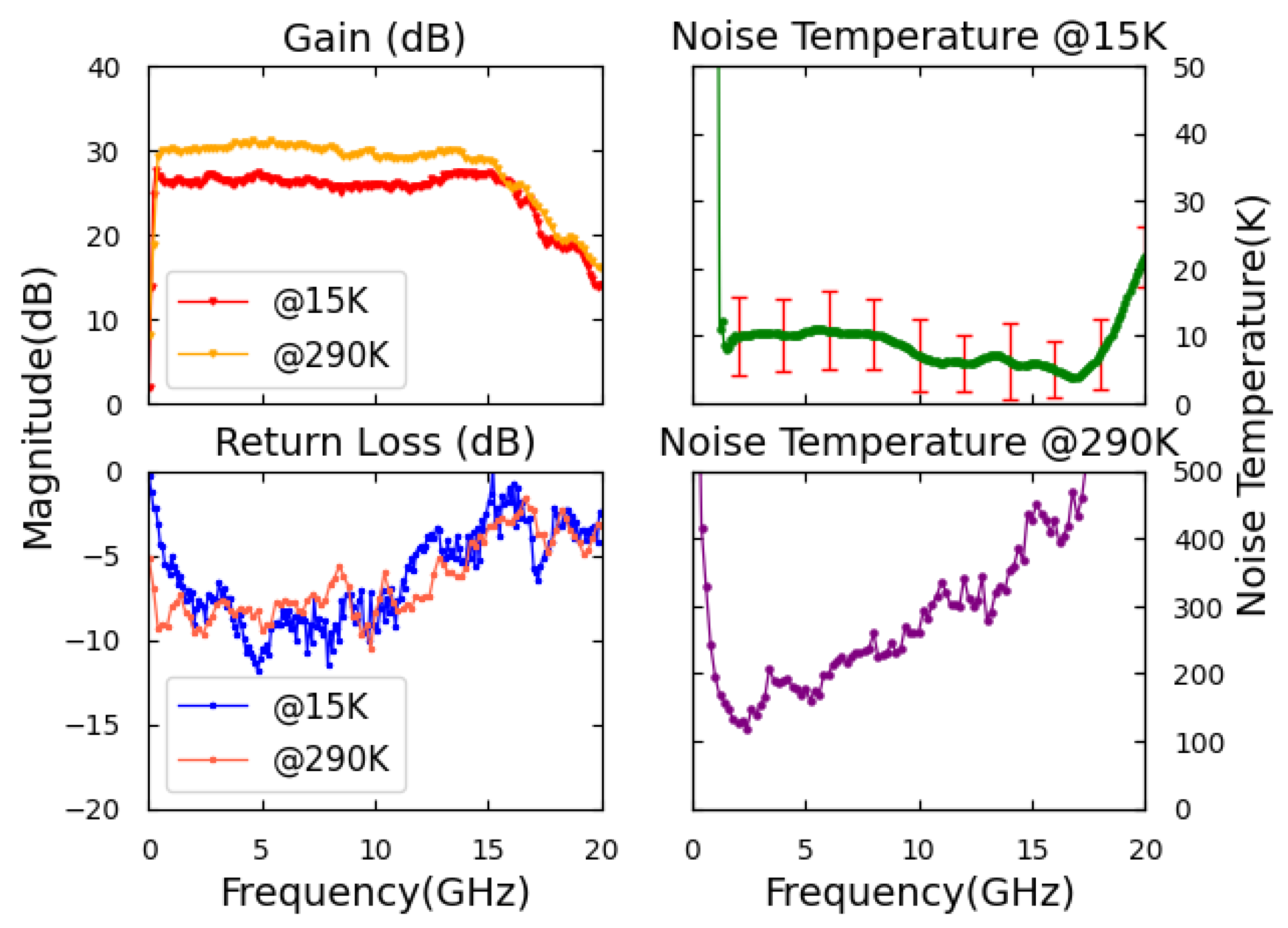
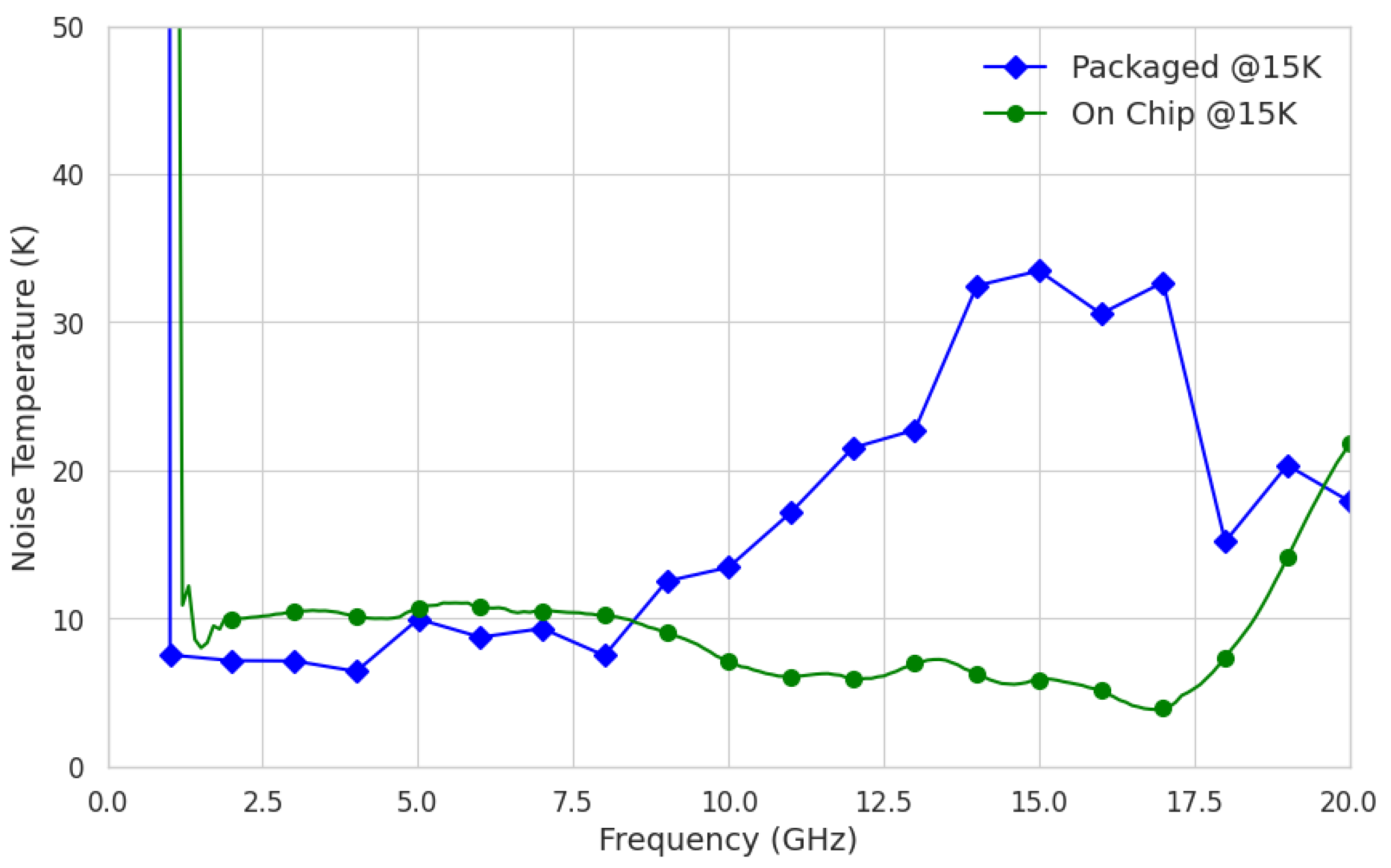
In conclusion, two-finger and four-finger transistors were DC characterized cryogenically. The two-finger and the small four-finger devices showed smooth responses, whereas the large four-finger devices showed distortion under some specific bias. All transistors were tested with a light on and we noted that light stimulation’s impact can be neglected in a short period of observation. While photosensitivity characterization under optical illumination was not implemented in this study, prior investigations by Alina Caddemi provide critical insights into photostimulation effects on transistors and amplifiers [6,7].

3. Results

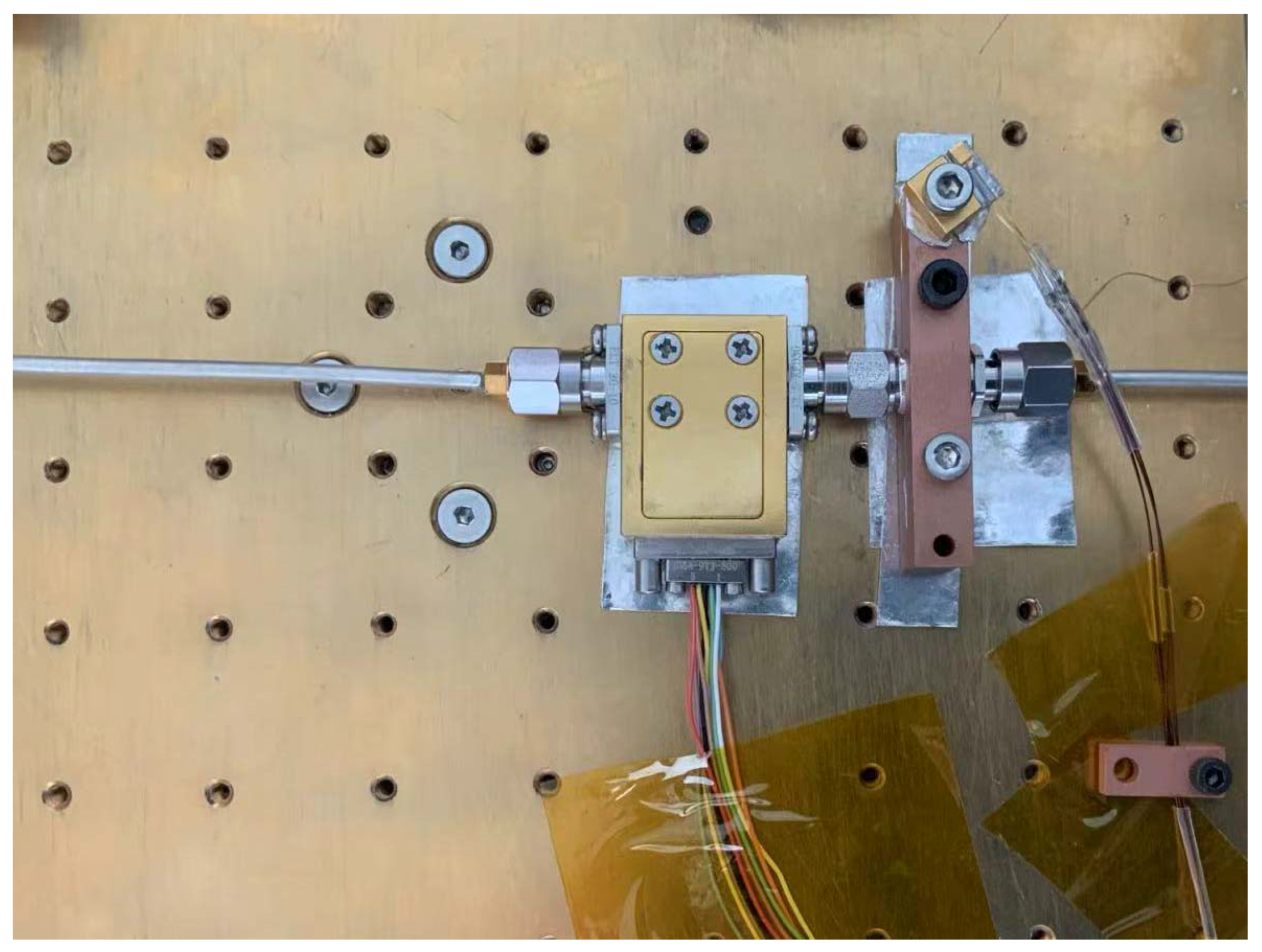
LNA Design and Measurements

Two low-noise amplifiers were designed and fabricated in this work, namely LNA0315 and LNA0307, covering frequencies from 0.3 to 15 GHz and 0.3–7 GHz, respectively. The chip photographs of the LNA MMIC are shown in Figure 3. The LNA0315 occupies a chip area of 3 × 1 mm 2 , and the LNA 0307 occupies 3 × 1.5 mm 2 .
Both LNAs are designed with three stages of common-source configurations. This particular topology is favored for its robust stability, which is especially beneficial at cryogenic temperatures. The simplicity of the design aids in matching and biasing the components. In scenarios where transistor characteristics become unpredictable under cryogenic conditions, the common-source approach proves to be a reliable option. The LNAs incorporate MS-type transistors, chosen for their slightly lower noise profile compared to CPW-type counterparts. A distinctive feature of the MS-type transistors is their source end connection to the ground (GND) via two vias, as depicted in Figure 1. This can be regarded as source degeneration inductors, which contribute to the stabilization of the amplifiers. Selecting the gate width and the number of gate fingers is pivotal to the LNA’s performance. Adjusting the number of transistor fingers helps in selecting the appropriate device impedances, which is essential for effective impedance matching and for boosting the output power capability of the transistor [8,9]. It is noteworthy that, despite the advantages, transistors with a multifingered structure may exhibit unstable operation at cryogenic temperatures, as previously mentioned. These instabilities are often hard to predict and can be challenging to verify with standard measurement techniques, as reported in the literature [10,11,12].
In this project, we selected a four-finger transistor with a cumulative gate periphery of 300 μ m for the LNA0315 design due to its optimal balance among noise characteristics, device impedance, and output power potential. For LNA0307, a selection of three distinct devices was made, comprising an eight-finger transistor with a 200 μ m gate periphery, as well as two four-finger transistors with gate peripheries of 400 μ m and 200 μ m, respectively. The rationale behind this arrangement was to initially assess the stability of these large devices under various conditions and to determine their impact on the LNA’s performance at cryogenic temperatures.
The input and output of the LNA are impedance matched using on-chip MIM capacitors and transmission lines. Resistors in parallel can fine-tune the impedances and also form part of the bias lines, in conjunction with MIM capacitors, to ensure stability. The first stage of the amplifier is meticulously designed to enhance matching and to minimize noise. Its bias voltage is set separately from the others for ease of adjustment. The subsequent stages are responsible for maintaining gain flatness across the bandwidth.
There are many ways to measure noise temperature for packaged circuits or systems [13,14,15,16]; however, due to the cryogenic temperature, calibration error, and even oxidation of probes, significant challenges have been brought to on-wafer measurements. Ref. [17] achieved a cryogenic noise measurement uncertainty of ± 1.4 K using an attenuator MMIC bonded to the DUT—an approach we highly recommend. The integrated attenuator effectively mitigates errors induced by both the noise diode and input transmission line, while simultaneously stabilizing impedance variations during on/off switching of the diode noise source. However, limited by our laboratory’s equipment, a simplified noise measurement based on the Y-factor method is applied for getting a quick approximation on noise performance.
S-parameter and noise measurements of the LNAs were first performed in the probe station with a Keysight Technologies vector network analyzer (VNA) and a noise figure analyzer (NFA). The VNA is calibrated using SOLT (short-open-load-through) method with a GGB calibration substrate at RT. Furthermore, a calibration chip fabricated based on the same process with LNAs is used to de-embed the cryogenic S-parameters. A noise source with a specified excess noise ratio (ENR) is connected to the DUT via the input probe arm to supply two different noise power at on/off state. There is a premised assumption that the probe arms before and after DUT have to be totally equal, since they are de-embedded and as a result measured together using the VNA. To calculate the equivalent noise of the path between the noise source and the DUT, two parameters must be known: the loss and the physical temperature of the path. The loss can be measured by VNA. A calibration chip’s Through kit was used to implement this measurement, which can be treated as an ideal connection without loss between the two probes. As for the physical temperature of the path, a precise sensor (DT-670 Series silicon diodes of Lakeshore probe station) mounted on the probe arm was used to measure the temperature in the probe station. The physical temperature of the path outside of the cryogenic chamber is 290 K. Nevertheless, since the temperature gradient exists, the equivalent noise temperature obtained still has errors, which can be estimated as δ T input . Then, controlling the probes to measure the DUT, the total system’s noise temperature and the DUT gain can be measured, respectively. Using Friis’ Equation [18], the noise temperature of the DUT is given by T DUT ,
T DUT = G input ( ( E N R × T 0 + T s off ) T s off Y ) Y 1 T output G DUT G input T input .
where G input and G DUT are the gains of the input path and the DUT, respectively, T input and T output are the effective noise temperature of the input and output path, respectively, and T s off is the temperature of the noise source at off state. The major uncertainty comes from the ENR referred as δ E N R of 0.1 dB, and the measurement error of the Y-factor δ Y of 0.02 dB. The available gain and the effective temperature uncertainty of the input path are δ G input and δ T input . Other less impact items were neglected and the Root Sum of Squares method was used for estimation, as shown in Equation (2).
δ T DUT = T DUT ENR δ ENR 2 + T DUT Y δ Y 2 + T DUT G input δ G input 2 + T DUT T input δ T input 2 ,
The uncertainty of the temperature of two types of DUTs at cryogenic are about ± 5.5 K and ± 11 K , respectively. The novel approach used here is a simple but compromised method under current conditions. The measurement results after packaging will be more convinced which are now in progress. The following are the results obtained so far.
Figure 4 presents the measured scattering parameter and noise temperature of the LNA0315 at 290 K and 15 K, respectively. The measured noise is ≤10 K from 2 to 15 GHz at 15 K, decreased by more than an order of magnitude compared to of noise measured at 290 K. Over the bandwidth, the average gain is about 30 dB at 290 K and 26 dB at 15 K, since the total I d = 44 mA under 0.7 V supply voltage and the power consumption is about 30 mw at 15 K lower than 90 mw at 290 K with a total I d = 60 mA under 1.5 V supply voltage. The average input return loss is about 6 dB at 290 K and 10 dB at 15 K over most of the bandwidth.
Figure 5 illustrates the results of LNA0307 measurements. A large transistor having eight fingers connected with a spiral inductor is used as the first stage. Cryogenic noise temperature is about 10–20 K, which is an order of magnitude lower than results at RT. The power consumption is about 40 mw at 15 K and 100 mW at 290 K. The total I d = 56 mA under 0.7 V supply voltage at 15 K and I d = 66 mA under 1.5 V supply voltage at 290 K. The measured gain is approximately 30 dB, while the gain flatness is not very good at 15 K. The input return loss is better than 10 dB from 2 to 6 GHz at 15 K and about 6 dB at RT. It is worth noting that LNA0307 is more sensitive to changes in bias, which is likely because the large transistor in the eight-finger device encountered DC and RF instabilities more frequently in cryogenic operation [8,10].
The LNS0315 was packaged as shown in Figure 6 and Figure 7. Then, they measured the noise temperature using a 20 dB attenuator method at the cryogenic test bed in a cryogenic Dewar, as shown in Figure 8. Two temperature sensors are located under the test bed and on the attenuator fixture, respectively. The outer input end of the Dewar is connected with a noise source. The output of the DUT is connected to an NFA. Comparing the noise temperature results of bare chip and packaged, it can be concluded as shown in Figure 9. The two lines coincide well when the frequency is less than 10 GHz. However, the noise temperature of packaged one begins to deteriorate after more than 10 GHz. It may be that the package causes the noise to change greatly in the high frequency band. In view of the large error in the use of on-chip testing methods, packaged results are more reliable. The packaged LNA0315 achieves noise performance of around 10 K in the 2–10 GH range.

4. Discussion

Table 1 gives a rough comparison of state-of-art cryogenic LNAs and this work, including the commercial LNAs. The FoM (Figure of Merit) was defined as [19]
FOM = Gain [ Lin ] · BW [ GHz ] ( NF [ Lin ] 1 ) · P dc [ mW ] ,
To the best of the authors’ knowledge, the 180 nm pHMET from WIN is seldom utilized at cryogenic temperatures for radio astronomy. This is because researchers generally prefer transistors with short gate lengths, as they have been proven to exhibit lower noise levels compared to those with longer gate lengths normally at room temperature. From the overall performance of those two kinds of LNAs, the bandwidths are wide enough to cover the radio frequencies of interest up to the Ku band, and the gain is high enough to provide good performance for the intended applications. The noise temperatures are reasonable, and the power consumption is also within the range of the cryogenic applications. What cannot be ignored is that its cost is more advantageous.
Though the scope of this study is limited, the early results are promising and demonstrate the potential of this process for cryogenic temperature applications. The observed performance enhancements at low temperatures suggest that this technology could be a strong contender for future research and development in the field of cryogenic electronics. With further investigation, this process may pave the way for innovative solutions in areas such as radio astronomy and cryogenic technology.

5. Conclusions

In this work, we characterized discrete transistors fabricated using WIN’s pHEMT process at both room and cryogenic temperatures. Upon cooling to 15 K, the two-finger devices exhibited minor changes, including an increase in peak transconductance and a decrease in drain current density under lower bias conditions. Similar variations were observed in the four-finger devices with shorter gate widths. In contrast, the large four-finger devices, particularly those with total gate peripheries exceeding 300 μ m, showed an unsmooth response at lower bias. Due to experimental constraints, further investigation is required to elucidate the mechanisms behind these phenomena.
Additionally, we detail the performance characteristics of two ultra-wideband cryogenic MMIC LNAs, and packaged the better one, positioning them as promising candidates for application in QTT telescope receivers. The first LNA demonstrated a noise temperature of ≤10 K across the 2 to 10 GHz frequency range, while the second achieved ≤20 K from 2 to 7 GHz. Compared to room temperature (RT) measurements, the noise levels dropped significantly, by an order of magnitude. The gain of the LNAs was measured to be 26 dB and 30 dB at 15 K, respectively. Power consumption was reduced to one-third of the RT levels. Owing to their broadband capabilities and low-noise performance, both amplifiers are suitable for use in radio telescope receivers. Further optimization of noise temperature (<5 K target) and input return loss (>15 dB) can be achieved through iterative refinement of the existing matching network, topology and packaging, leveraging the measured S-parameters and DC data at 15 K, while streamlined cryogenic testing protocols may accelerate LNA development cycles. The process-refined LNAs will be deployed in prototype cryogenic receiver modules for the QTT’s phased-array feed.

Author Contributions

Conceptualization, M.C.; Methodology, H.W.; Validation, M.C.; Writing—original draft, H.W. All authors have read and agreed to the published version of the manuscript.

Funding

This work was funded by the National Key R&D Program of China, No. 2022YFC2205301.

Data Availability Statement

All data supporting the findings of this study are available from the corresponding author upon reasonable request.

Conflicts of Interest

The authors declare no conflicts of interest.

References

  1. McCulloch, M.A.; Grahn, J.; Melhuish, S.J.; Nilsson, P.A.; Piccirillo, L.; Schleeh, J.; Wadefalk, N. Dependence of Noise Temperature on Physical Temperature for Cryogenic Low-Noise Amplifiers. J. Astron. Telesc. Instruments Syst. 2017, 3, 014003. [Google Scholar] [CrossRef]
  2. Chiong, C.C.; Wang, Y.; Chang, K.C.; Wang, H. Low-Noise Amplifier for Next-Generation Radio Astronomy Telescopes: Review of the State-of-the-Art Cryogenic LNAs in the Most Challenging Applications. IEEE Microw. Mag. 2022, 23, 31–47. [Google Scholar] [CrossRef]
  3. Wang, N. Xinjiang Qitai 110 m Radio Telescope. Sci. Sin. Phys. Mech. Astron. 2014, 44, 783–794. [Google Scholar] [CrossRef]
  4. Wang, N.; Xu, Q.; Ma, J.; Liu, Z.; Liu, Q.; Zhang, H.; Pei, X.; Chen, M.; Manchester, R.N.; Lee, K.; et al. The Qitai Radio Telescope. Sci. China Phys. Mech. Astron. 2023, 66, 289512. [Google Scholar] [CrossRef]
  5. Shell, J. The Cryogenic DC Behavior of Cryo3/AZ1 InP 0.1-by-80-Micrometer-Gate High Electron Mobility Transistor Devices. IPN Prog. Rep. 2007, 42–169, 1–26. [Google Scholar]
  6. Caddemi, A.; Cardillo, E.; Patanè, S.; Triolo, C. Light Exposure Effects on the DC Kink of AlGaN/GaN HEMTs. Electronics 2019, 8, 698. [Google Scholar] [CrossRef]
  7. Caddemi, A.; Cardillo, E.; Patanè, S.; Triolo, C. An Accurate Experimental Investigation of an Optical Sensing Microwave Amplifier. IEEE Sens. J. 2018, 18, 9214–9221. [Google Scholar] [CrossRef]
  8. Varonen, M.; Reeves, R.; Kangaslahti, P.; Samoska, L.; Kooi, J.W.; Cleary, K.; Gawande, R.S.; Akgiray, A.; Fung, A.; Gaier, T.; et al. An MMIC Low-Noise Amplifier Design Technique. IEEE Trans. Microw. Theory Tech. 2016, 64, 826–835. [Google Scholar] [CrossRef]
  9. Varonen, M.; Reeves, R.; Kangaslahti, P.; Samoska, L.; Akgiray, A.; Cleary, K.; Gawande, R.; Fung, A.; Gaier, T.; Weinreb, S.; et al. A 75–116-GHz LNA with 23-K Noise Temperature at 108 GHz. In Proceedings of the 2013 IEEE MTT-S International Microwave Symposium Digest (MTT), Seattle, WA, USA, 2–7 June 2013; pp. 1–3. [Google Scholar] [CrossRef]
  10. Moschetti, G.; Thome, F.; Ohlrogge, M.; Goliasch, J.; Schäfer, F.; Aja, B.; Leuther, A.; Schlechtweg, M.; Seelmann-Eggebert, M.; Ambacher, O.; et al. Stability Investigation of Large Gate-Width Metamorphic High Electron-Mobility Transistors at Cryogenic Temperature. IEEE Trans. Microw. Theory Tech. 2016, 64, 3139–3150. [Google Scholar] [CrossRef]
  11. Rodilla, H.; Schleeh, J.; Nilsson, P.A.; Grahn, J. Cryogenic Kink Effect in InP pHEMTs: A Pulsed Measurements Study. IEEE Trans. Electron Devices 2015, 62, 532–537. [Google Scholar] [CrossRef]
  12. Yang, Q. Low Frequency Dispersion in InP HEMTs. Master’s Thesis, Chalmers University of Technology, Göteborg, Sweden, 2013. [Google Scholar]
  13. Keysight. Noise Figure Measurement Accuracy: The Y-Factor Method. 2021. Available online: https://www.keysight.com/us/en/assets/7018-06829/application-notes/5952-3706.pdf (accessed on 15 October 2024).
  14. Keysight. High-Accuracy Noise Figure Measurements with Network Analyzers. 2020. Available online: https://www.keysight.com/us/en/assets/7018-02539/application-notes/5990-5800.pdf (accessed on 15 October 2024).
  15. Fernandez, J.E. A Noise-Temperature Measurement System Using a Cryogenic Attenuator. TMO Prog. Rep. 1998, 15, 42–135. [Google Scholar]
  16. Sheldon, A.; Belostotski, L.; Mani, H.; Groppi, C.E.; Warnick, K.F. Cryogenic Noise-Parameter Measurements: Recent Research and a Fully Automated Measurement Application. IEEE Microw. Mag. 2021, 22, 52–64. [Google Scholar] [CrossRef]
  17. Heinz, F.; Thome, F.; Leuther, A.; Ambacher, O. A Cryogenic On-Chip Noise Measurement Procedure With ±1.4-K Measurement Uncertainty. In Proceedings of the 2022 IEEE/MTT-S International Microwave Symposium-IMS, Denver, CO, USA, 19–24 June 2022; pp. 233–236. [Google Scholar] [CrossRef]
  18. Friis, H. Noise Figures of Radio Receivers. Proc. IRE 1944, 32, 419–422. [Google Scholar] [CrossRef]
  19. Shiramizu, N.; Masuda, T.; Tanabe, M.; Washio, K. A 3–10 GHz Bandwidth Low-Noise and Low-Power Amplifier for Full-Band UWB Communications in 0.25-/Spl Mu/m SiGe BiCMOS Technology. In Proceedings of the 2005 IEEE Radio Frequency Integrated Circuits (RFIC) Symposium-Digest of Papers, Long Beach, CA, USA, 12–14 June 2005; pp. 39–42. [Google Scholar] [CrossRef]
  20. Akgiray, A.H.; Weinreb, S.; Leblanc, R.; Renvoise, M.; Frijlink, P.; Lai, R.; Sarkozy, S. Noise Measurements of Discrete HEMT Transistors and Application to Wideband Very Low-Noise Amplifiers. IEEE Trans. Microw. Theory Tech. 2013, 61, 3285–3297. [Google Scholar] [CrossRef]
  21. Heinz, F.; Thome, F.; Leuther, A.; Ambacher, O. A 50-Nm Gate-Length Metamorphic HEMT Technology Optimized for Cryogenic Ultra-Low-Noise Operation. IEEE Trans. Microw. Theory Tech. 2021, 69, 3896–3907. [Google Scholar] [CrossRef]
  22. Wong, W.T.; Coskun, A.H.; Bardin, J.C. Design and Characterization of a Wideband High-Dynamic Range SiGe Cryogenic Low Noise Amplifier. In Proceedings of the 2017 IEEE MTT-S International Microwave Symposium (IMS), Honololu, HI, USA, 4–9 June 2017; pp. 1972–1975. [Google Scholar] [CrossRef]
  23. Low Noise Factory AB, L.N.F.A. LNF-LNC0.3_14B. 2023. Available online: https://lownoisefactory.com/product/lnf-lnc0-3_14b/ (accessed on 6 April 2025).
  24. Bardin, J.C.; Weinreb, S. A 0.1–5 GHz Cryogenic SiGe MMIC LNA. IEEE Microw. Wirel. Compon. Lett. 2009, 19, 407–409. [Google Scholar] [CrossRef]
  25. Peng, Y.; Zhong, Y.; Guo, Z.; Liu, S.; Yu, D. A 3.5 7.5 GHz GaAs HEMT Cryogenic Low-NoiseAmplifier Achieving 5 Kelvin Noise Temperature for Qubits Measurement. In Proceedings of the 2023 IEEE/MTT-S International Microwave Symposium-IMS, San Diego, CA, USA, 11–16 June 2023; pp. 672–675. [Google Scholar] [CrossRef]
  26. Wang, Y.; Chiong, C.C.; Nai, J.K.; Wang, H. A High Gain Broadband LNA in GaAs 015-Mm pHEMT Process Using Inductive Feedback Gain Compensation for Radio Astronomy Applications. In Proceedings of the 2015 IEEE International Symposium on Radio-Frequency Integration Technology (RFIT), Sendai, Japan, 26–28 August 2015; pp. 79–81. [Google Scholar] [CrossRef]
  27. Chen, P.S.; Kim, D.H.; Bergman, J.; Hacker, J.; Brar, B. Wideband Low-Noise-Amplifier (LNA) with Lg = 50 Nm InGaAs pHEMT and Wideband RF Chokes. In Proceedings of the 2011 IEEE MTT-S International Microwave Symposium, Baltimore, MD, USA, 5–10 June 2011; pp. 1–5. [Google Scholar] [CrossRef]
  28. Zhang, H.; Qian, G.; Zhong, W.; Liu, C. A 3–15 GHz Ultra-Wideband 0.15-Mm pHEMT Low Noise Amplifier Design. In Proceedings of the 2016 IEEE International Conference on Communication Systems (ICCS), Shenzhen, China, 14–16 December 2016; pp. 1–4. [Google Scholar] [CrossRef]
  29. Lei, H.W.; Wang, Y.; Chiong, C.C.; Wang, H. A 2.5–31-GHz High Gain LNA in 0.15-Mm GaAs pHEMT for Radio Astronomical Application. In Proceedings of the 2018 Asia-Pacific Microwave Conference (APMC), Kyoto, Japan, 6–9 November 2018; pp. 228–230. [Google Scholar] [CrossRef]
Figure 1. (a) Micrographs of discrete transistors with varying gate numbers (2, 4) and gate widths (25, 50, 75, 100, 125, 150 μ m). Each chip contains an MS-type (up) and a CPW-type (down) transistor. (b) The zoomed-in micrograph of a two-finger device with a gate width of 50 μ m devices (2f100 μ m).
Electronics 14 01572 g001
Figure 2. I d V d s characteristics and DC transconductance of the 4f600 μ m and 2f50 μ m transistors at (a,c,e,g) 15 K and (b,d,f,h) 290 K. The transistor type appears in the lower right corner of Figure 1.
Electronics 14 01572 g002
Figure 3. Schematic of the (a) LNA0315, (c) LNA0307 and chip photograph of the three-stage (b) LNA0315 occupied an area of 3 × 1 mm 2 (d) LNA0307 occupied an area of 3 × 1.5 mm 2 .
Electronics 14 01572 g003
Figure 4. Comparison of the measurements at 290 K and 15 K of the LNA0315. The gain, the input return loss, and the noise temperature are plotted.
Electronics 14 01572 g004
Figure 5. Comparison of the measurements at 290 K and 15 K of the LNA0307. The gain, the input return loss, and the noise temperature are plotted.
Electronics 14 01572 g005
Figure 6. The inside of the packaged LNA.
Electronics 14 01572 g006
Figure 7. The micrograph shows the LNA chip in its package.
Electronics 14 01572 g007
Figure 8. The measurement setup for the packaged LNA.
Electronics 14 01572 g008
Figure 9. Comparison of the noise measurements at 15 K of the LNA0315 chip and the packaged LNA0315.
Electronics 14 01572 g009
Table 1. Comparisons of state-of-art cryogenic LNAs and this work.
Ref.TechnologyFreq. (GHz)Gain (dB)Noise Temp. (K) P dc ( mw ) FoM
[20]OMMIC GaAs 70 nm mHEMT0.7–162410 @20 K16 @20 K480
[20]NGC InP 35 nm pHEMT1–2022–2510 @22 K30 @22 K312
[21]GaAs 50 nm mHEMT8–1839.43.3–5.6 @10 K24.4 @10 K8021
[22]120 nm BiCMOS1–2023–279–30 @17 K60 @17 K85
[23]module0.3–14373.6 @5 K19.2 @5 K4967
[24]IBM SiGe 130 nm BiCMOS0.1–529.64.3 @15 K20 @15 K779
[25]discrete GaAs HEMT3.5–7.5>30<12 @3.6 K19 @3.6 K63
[26]150 nm GaAs pHEMT3.2–14.734101@RT 45 @RT1839
[27]50 nm InP pHEMT4–241784 @RT20 @RT174
[28]150 nm GaAs pHEMT3–1528226 @RT200 @RT49
[29]150 nm GaAs pHEMT2.5–3132.7129 @RT60 @RT1985
This workWIN 180 nm GaAs pHEMT0.3–15265–10 @15 K30 @15 K980
This workWIN 180 nm GaAs pHEMT0.3–73015–20 @15 K40 @15 K233
RT: room temperature.
Disclaimer/Publisher’s Note: The statements, opinions and data contained in all publications are solely those of the individual author(s) and contributor(s) and not of MDPI and/or the editor(s). MDPI and/or the editor(s) disclaim responsibility for any injury to people or property resulting from any ideas, methods, instructions or products referred to in the content.

