Abstract
Wireless power transfer (WPT) is extensively utilized because of its isolation and convenience. However, WPT systems require different types of outputs in specific applications. The existing dual-receiving WPT system has disadvantages such as redundant compensation components, unnecessary cross-coupling interference, complex control circuits, and low space utilization. To address these shortcomings, this paper proposes a dual-output WPT system capable of delivering both constant voltage (CV) and constant current (CC) outputs simultaneously. The WPT system utilizes a special coil structure design, in which the DD coil is used as the transmitter coil and the first receiver coil, and the Q coil is used as the relay coil and the second receiver coil. In addition, the DD coil and the Q coil can achieve natural decoupling under alignment conditions. Consequently, the impact of the unnecessary cross-coupling within the system can be eradicated. Initially, the natural decoupling properties of the magnetic coupler are analyzed from a theoretical perspective. Subsequently, a mathematical model for the proposed WPT system is constructed. Through theoretical deductions, it is demonstrated that under the zero-phase-angle (ZPA) conditions, the system is capable of attaining a CC output at the first receiving side and a CV output at the second receiving side. Finally, a verification experimental prototype with a constant voltage output of 72 V and a constant current output of 2.5 A was built. The experimental results verified the accuracy of the previous theoretical analysis.
1. Introduction
As a convenient and efficient way of energy transmission, wireless power transmission (WPT) technology has shown great application potential and development background in the fields of consumer electronics [1,2], implantable medical devices [3,4], and industrial automation [5,6]. WPT systems with a constant current (CC) output function are widely used in fields such as LED driving [7,8,9], and WPT systems with a constant voltage (CV) output function are extensively utilized in fields such as mobile device power supply [10,11,12]. However, it has been difficult for the traditional single-output WPT system to meet the energy supply needs in complex scenarios. WPT systems with CC and CV dual outputs have gradually become a research hotspot. Unnecessary cross-coupling will affect the stability of the system [13,14]. Therefore, reducing or eliminating unnecessary cross-coupling between systems is the key to building a stable dual-output WPT system.
To solve the above problems, in [15,16], researchers proposed placing multiple receivers at a distance from one another to reduce the impact of cross-coupling. However, these methods greatly reduce the utilization of system space; moreover, the coupling interference cannot be completely eliminated. To satisfy more practical requirements and improve system space utilization, authors adopted the method of magnetic shielding to suppress coupling interference by adding metal insulators around the coil [17,18], but these methods increased the overall volume and weight of the system. Regarding the above problems, the method of using decoupling reactance is proposed in [19,20]. By connecting the two receiving sides together using passive components, the effects of cross-coupling can be eliminated. But these methods make it difficult for the two receiving sides of the system to move. In order to improve the system’s freedom of movement, Zhong et al. in [21], Gong et al. in [22], and Qi et al. in [23] eliminated the interference of cross-coupling by changing the system’s resonant frequency. However, these methods cause frequency bifurcation in the system, thereby reducing system stability and reliability.
Therefore, specially designed magnetic couplers are being introduced into dual-output WPT systems. Through an appropriate design of the structure of the coils and positions, the influence of coupling interference can be eliminated. A bucking planar coil (BPC) is proposed in [24]. By changing the BPC direction, the magnetic flux is canceled, thus achieving decoupling. However, the number of turns of the BPC requires a special design, which greatly reduces the design freedom of the system. Based on the above issues, a dual-output system is proposed in [25]. As the magnetic flux flowing through the two mutually perpendicular solenoid coils tends to zero, it effectively eliminates the influence of cross-coupling. Moreover, the integration of the two solenoid coils onto the ferrite plate of the first receiving side greatly enhances the utilization of the system’s space.
To address the drawbacks of the aforesaid dual-output WPT system, including insufficient space utilization in [15,16]; metal insulators and excessive compensation components leading to increased system weight and cost in [17,18,25]; the system’s receiving side finding it difficult to move in [19,20]; the system having poor stability in [21,22,23]; and the complex design approach to the magnetic coupler in [24], this paper proposes a WPT system with CC and CV dual outputs. The transmitter coil and the first receiver coil are composed of two DD coils, and the relay coil and the second receiver coil are made up of two Q coils. Meanwhile, the first receiver coil and the relay coil are combined onto the ferrite plate on the first receiving side. The transmitting side utilizes the S compensation topology, the first receiving side utilizes the LCL compensation topology, and the second receiving side utilizes the S compensation topology. The proposed dual-output WPT system has the advantages of high space utilization, fewer compensation elements, an efficient transmission process, high system stability, and a simple magnetic coupler structure. At the same time, under ZPA conditions, the system is capable of achieving dual outputs of CC and CV that are independent of the load.
The structure of the manuscript is as follows. In Section 2, the proposed magnetic coupler is presented, and a detailed analysis of its decoupling characteristics is carried out. Section 3 presents an analysis and a complete theoretical derivation of the proposed dual-output WPT system. Section 4 describes an experimental prototype with an output current of 2.5 A on the first receiving side and an output voltage of 72 V on the second receiving side. The practicality and correctness of the proposed dual-output WPT system are proven by the experimental results. In the end, Section 5 concludes this paper.
2. Theoretical Analysis of Magnetic Coupler
Figure 1 shows the magnetic flux distribution of the Q coil and the DD coil. The DD coil is composed of two D coils with opposite directions connected in series. When the excitation current is increased, the current directions of the two D coil are opposite. Therefore, the directions in which the two D coils generate magnetic fluxes are opposite to each other. Further, in the magnetic field, the magnetic flux caused by one coil being excited and passing through the other coil can be expressed as follows:
where B is the magnetic field strength of the DD coil, and S is the surface area of the DD coil perpendicular to the magnetic field direction. From the above analysis, it is noticeable that the two segments of the magnetic flux created by the DD coil, which are perpendicular to the X-Y plane upward and perpendicular to the X-Y plane downward, cancel each other out when flowing through the Q coil. Similarly, the magnetic fluxes from the Q coils also cancel each other when flowing through the DD coil. Furthermore, the correlation between the magnetic flux and the mutual inductance of the Q coil and the DD coil can be stated as follows:
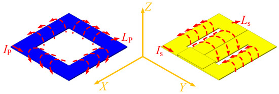
Figure 1.
Magnetic flux distribution of the Q coil and DD coil.
Therefore, the mutual induction between the DD coil and the Q coil is approximately zero, which means that the two coils are naturally decoupled.
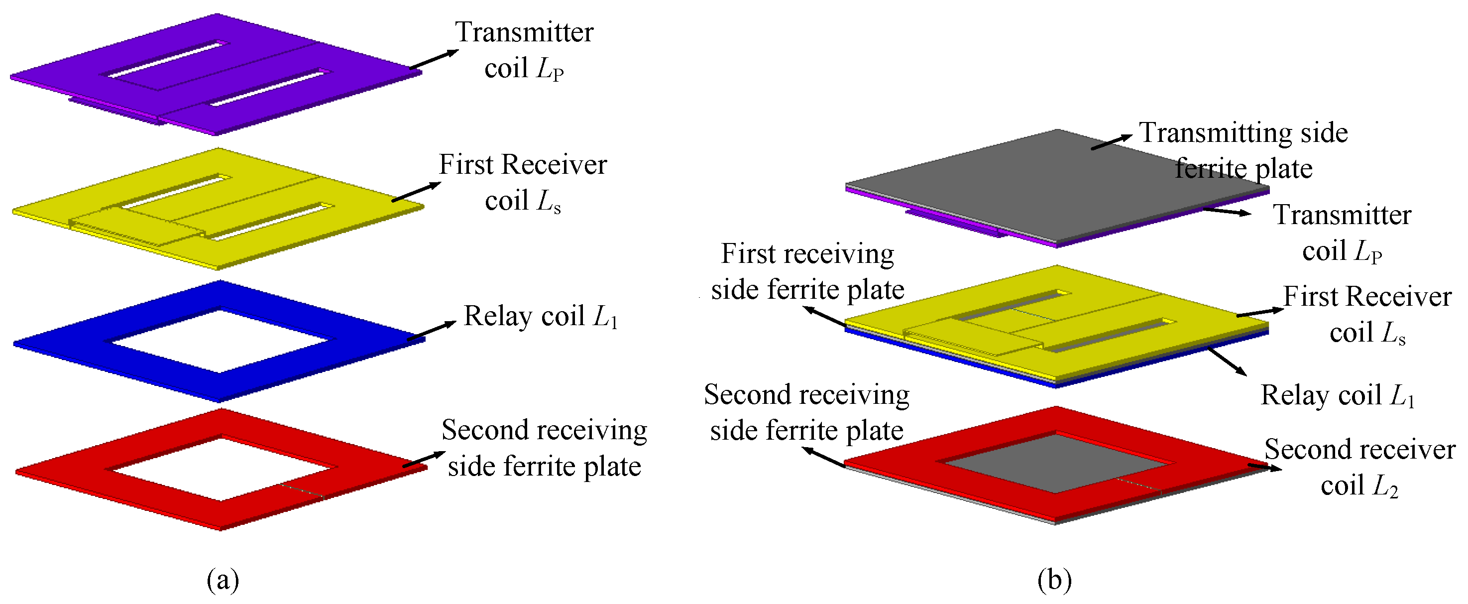
In summary, to eliminate the unnecessary cross-coupling in the dual-output WPT system, a magnetic coupler is proposed in this paper with a special decoupling design, as shown in Figure 2. The transmitter coil and the first receiver coil are both composed of DD coils; the relay coil and the second receiver coil are both composed of Q coils; and the relay coil and the first receiver coil are combined on the first receiving ferrite plate. Figure 3 shows the coupling effects between the proposed magnetic couplers. , , , , , and are the mutual inductances between and , and , and , and , and , and and , respectively. According to the above analysis, the value of the mutual inductance between the Q coil and the DD coil is approximately zero. It can be easily concluded that the mutual inductances , , , and are all approximately zero. In other words, the magnetic coupler that has been proposed is capable of eliminating the effects of unnecessary cross-coupling.

Figure 2.
Diagram presenting the proposed magnetic coupler. (a) Exploded view. (b) Complete view.
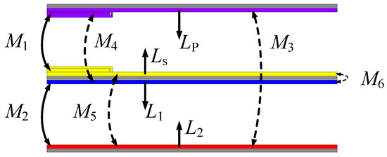
Figure 3.
Coupling effects between the proposed magnetic couplers.
3. Theoretical Analysis of the Proposed Dual-Output WPT System
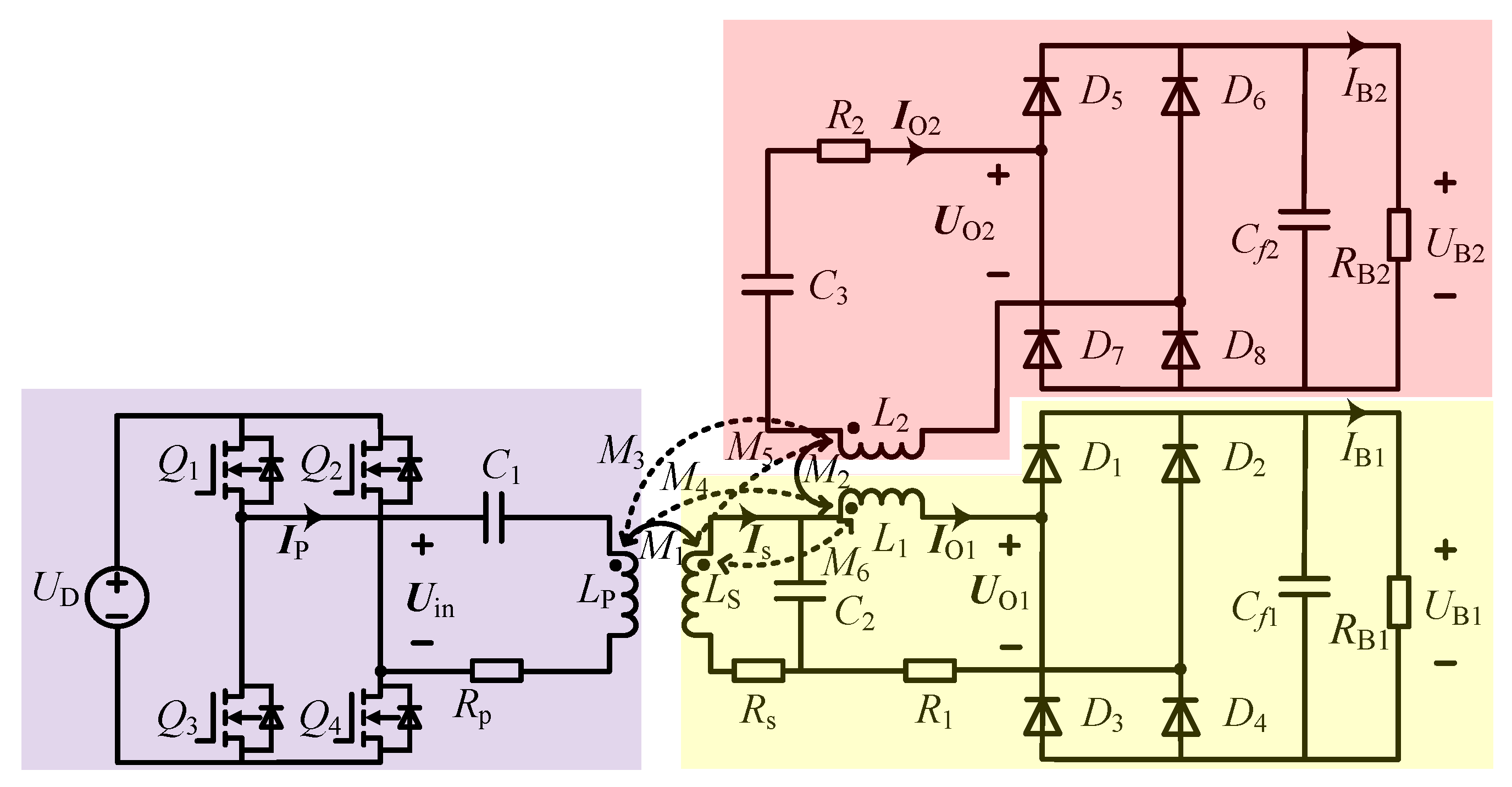
Shown in Figure 4 is the circuit architecture of the proposed WPT system with dual outputs. The direct current (DC) input voltage source is denoted as . The high-frequency inverter (HFI) is composed of four MOSFETs (–). , , and are the compensation capacitors of the circuit. The parasitic resistances of every coil are represented by , , , and . and are the filter capacitors of the two receiving sides. The two battery loads are represented by and . and are the two rectifier circuit input voltage phasors. , , , and are the current phasors of each branch. The diodes (–) and (–) form two full-bridge rectifier circuits, the purpose of which is to convert the AC current phasors and into DC output currents and , respectively. The relationship between the system DC input voltage and the root mean square (RMS) value of the AC output voltage phasors of the HFI can be expressed as follows [26]:
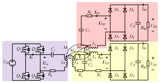
Figure 4.
Diagram of the overall circuit structure of the proposed dual-output WPT system.
In the rectifier circuit, the connection between the RMS value of the current phasor (voltage phasor ) and the battery charging current (charging voltage ) can be expressed as follows [26]:
To simplify the calculation, , , , , and are the impedances of the passive components in each loop, respectively, defined as follows:
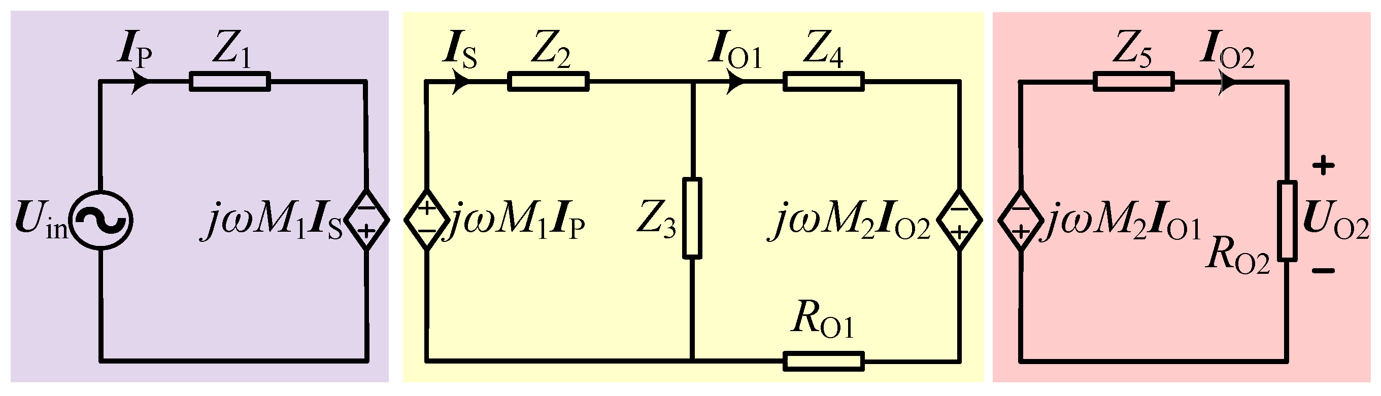
Figure 5 shows the equivalent circuit diagram of the system. For the purpose of facilitating further analysis, the internal resistance in the system is disregarded [27]. Based on Kirchhoff’s voltage law, the voltage expressions between different loops can be obtained as follows:
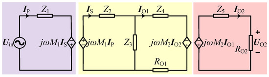
Figure 5.
Equivalent circuit diagram of dual-output WPT system.
The current phasors , and the voltage phasor can be calculated as follows:
where and are expressed as follows:
Based on (5), (7), and (8), to ensure that and are independent of and , A should be set to zero, that is,
Substituting (8) and (9) into (7), the input current phasor , output current phasor , and output voltage phasor can be expressed as follows:
In addition, in order to prevent the losses arising from the reactive circulating current, the system should implement a ZPA operation, that is, the imaginary part of the input impedance (=/) should be zero. From (10), the constraint condition for the system to implement a ZPA operation can be expressed as follows:
Therefore, can be expressed as follows:
According to (5), (9), and (11), the value of the compensation capacitor , , and can be calculated as follows:
From (10) and (12), it can be seen that the output current and the output voltage are independent of the loads. Furthermore, is purely resistive, which means that the system can achieve a ZPA operation.
4. Parameter Design and Simulation Verification
4.1. Parameter Design of the Proposed WPT System
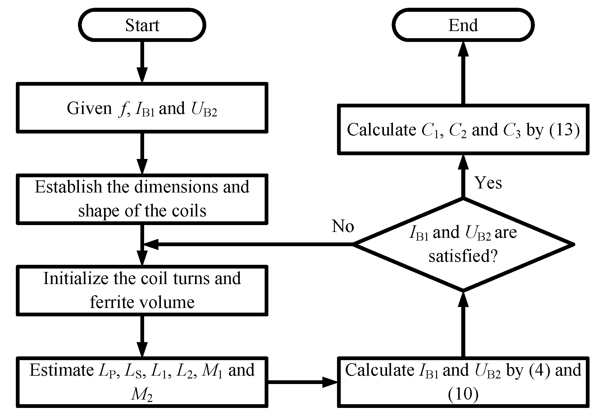
During the practical design phase, several iteration procedures are required to finalize the circuit parameters for the dual-output WPT system. The flowchart for the parameter design of the proposed WPT system is illustrated in Figure 6.
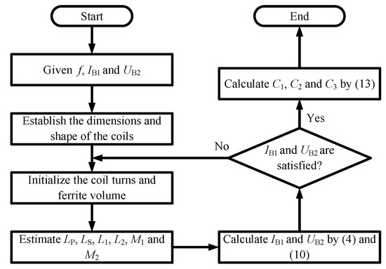
Figure 6.
Parameter design flowchart for the proposed WPT system.
Due to the parameter design approach mentioned above, the theoretical parameters of the proposed dual-output WPT system are presented in Table 1.

Table 1.
Theoretical parameters of the proposed dual-output WPT system.
4.2. Simulation Experiment Verification of the Proposed Dual-Output WPT System
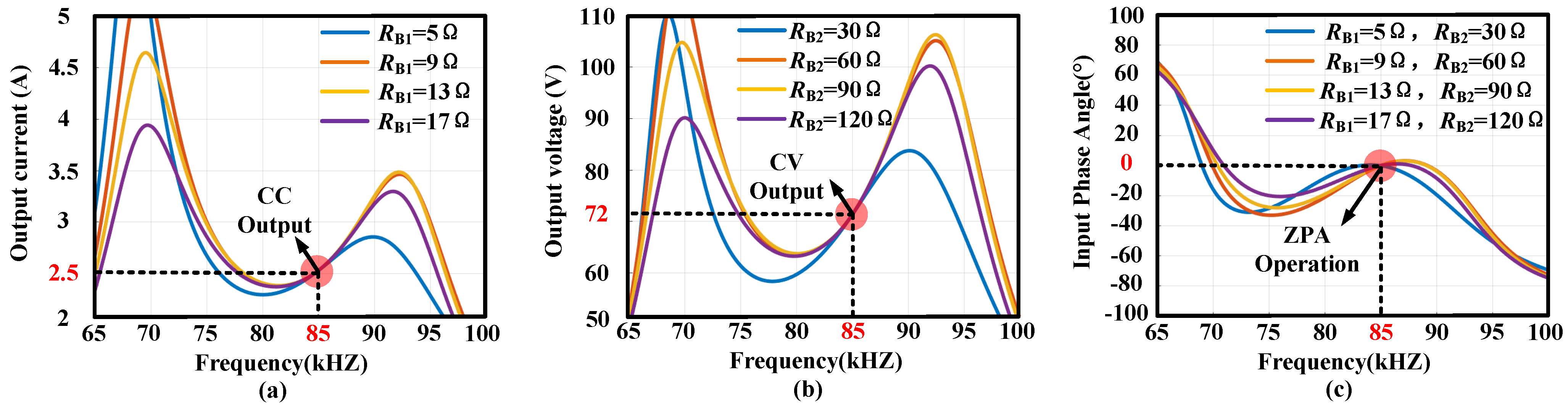
According to the detailed theoretical parameters designed in Table 1, the frequency sweeping curves of the output current , output voltage , and input impedance angle under different load conditions were obtained through MATLAB2020b simulation, as shown in Figure 7. As can be clearly seen from Figure 7, at an operating frequency of 85 kHz, the first receiving side and the second receiving side can obtain a CC output and a CV output, respectively. In addition, the system can attain a ZPA operation. From the simulation results shown above, the feasibility of the basic working characteristics of the propose dual-output WPT system is proven.
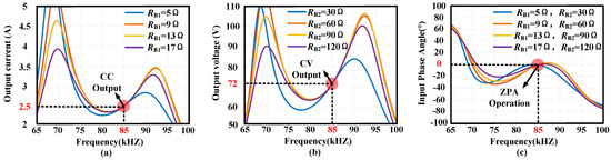
Figure 7.
Frequency scanning curves of the proposed dual outputs WPT system under different loads. (a) The first receiving side output current . (b) The second receiving side output voltage . (c) The input impedance angle.
5. Experimental Verification
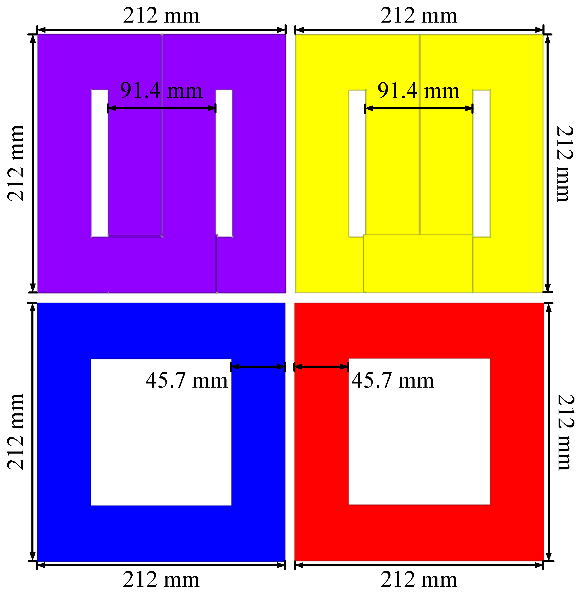
5.1. Magnetic Coupler Size Design
Due to the limitation of the actual installation space, the magnetic coupler dimensions in the WPT system require a rational design. The size of the magnetic coupler for the proposed dual-output WPT system is shown in Figure 8. The DD coil serves as the transmitter coil and the first receiver coil, and the Q coil serves as the relay coil and the second receiver coil. Among them, the relay coil and the first receiver coil are combined onto the ferrite plate on the first receiving side. Table 2 reveals the size parameters of the suggested magnetic coupler.

Figure 8.
Magnetic coupler size for the proposed dual-output WPT system.
Table 2.
Detailed parameters of the proposed dual-output WPT system’s magnetic coupler.
5.2. Experimental Prototype
To prove the correctness and rationality of the theoretical analysis for the proposed dual-output WPT system, a prototype for verification experiments with a CV output of 72 V and a CC output of 2.5 A was built, as shown in Figure 9. On the left side of the experimental platform is the DC input power supply , which provides a stable DC energy input for the entire system and is directly connected to the HFI. The high-frequency AC output of the HFI is connected to the transmitting side series compensation capacitor , which, together with the transmitting coil , constitutes the transmitting end circuit. The magnetic coupler, as the core component of the system, is in the middle position in the figure. The first receiving side’s parallel compensation capacitor is connected to the first receiving coil and is located on the side close to the magnetic coupler. The second receiving side’s series compensation capacitor is connected to the second receiving coil and is located on the other side of the experimental platform. The two full-bridge rectifier circuits are located at different positions of the experimental platform. The load resistors and simulate the load in actual applications and are connected to the output ends of the two full-bridge rectifier circuits, respectively. The oscilloscope is used to monitor the electrical signals of key nodes in the system and is connected to each test point through a probe, as shown in the figure. Table 3 provides the comprehensive parameters of the proposed dual-output WPT system.
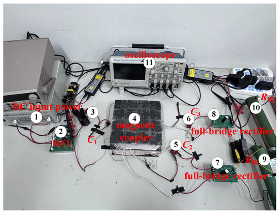
Figure 9.
Constructed experimental prototype for verification.
Table 3.
Detailed parameters of the proposed dual-output WPT system.
5.3. Experimental Results
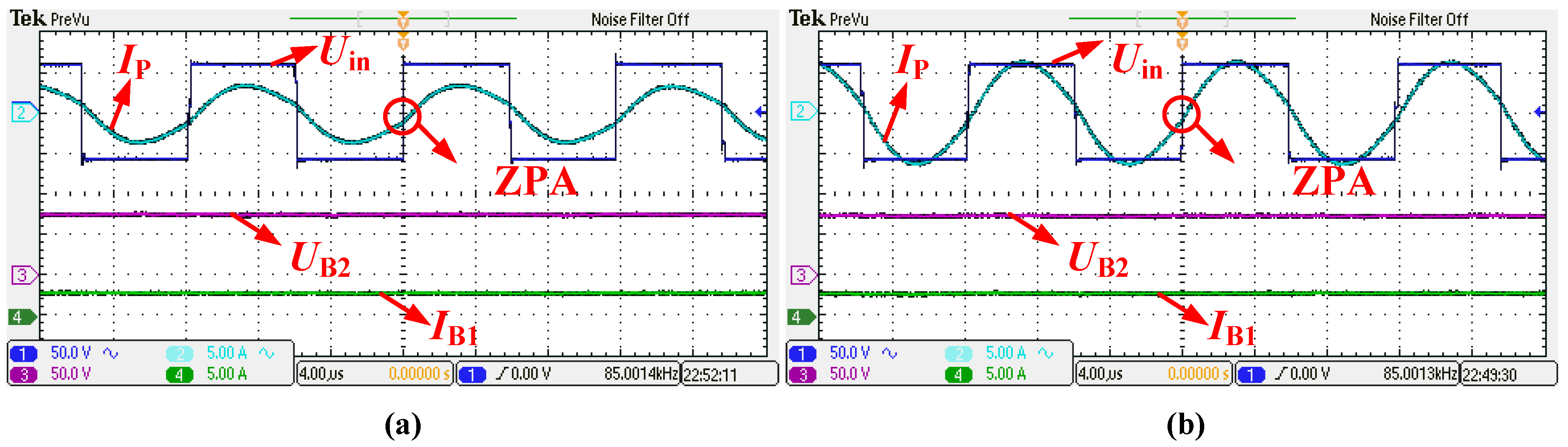
In Figure 10, the output voltage and current of the HFI, the output current of the first receiving side, and the output voltage of the second receiving side are presented. In Figure 10a, the load resistance of the first receiving side and the load resistance of the second receiving side are 5 and 30 , respectively. In Figure 10b, and are 10 and 60 , respectively. It is evident that under different load conditions, the system is capable of attaining a CC output of 2.5 A and a CV output of 72 V. In addition, under different combinations of and , the phase difference between and is always zero, which implies that the suggested system is capable of a ZPA operation.
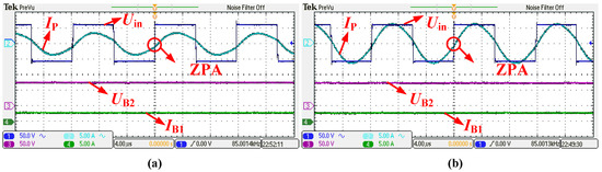
Figure 10.
Experimental waveforms of , , , and under ZPA conditions (a) = 5 , = 30 , (b) = 10 , = 60 .
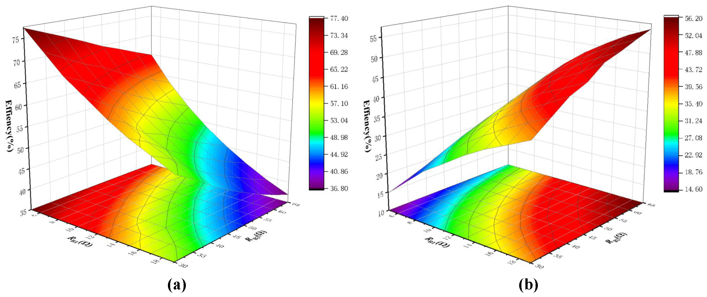
When the load changes from 5 to 19 in steps of 2 and the load changes from 30 to 65 in steps of 5 , 64 different combinations are measured, and the corresponding power distribution surface diagram is shown in Figure 11. It can be clearly seen that through a reasonable parameter design, the power distribution ratio of the first receiver and the second receiver can satisfy the complementary relationship and change evenly with the changes in the two loads.

Figure 11.
Power distribution ratio surface. (a) The power distribution ratio of the first receiver; (b) the power distribution ratio of the second receiver.
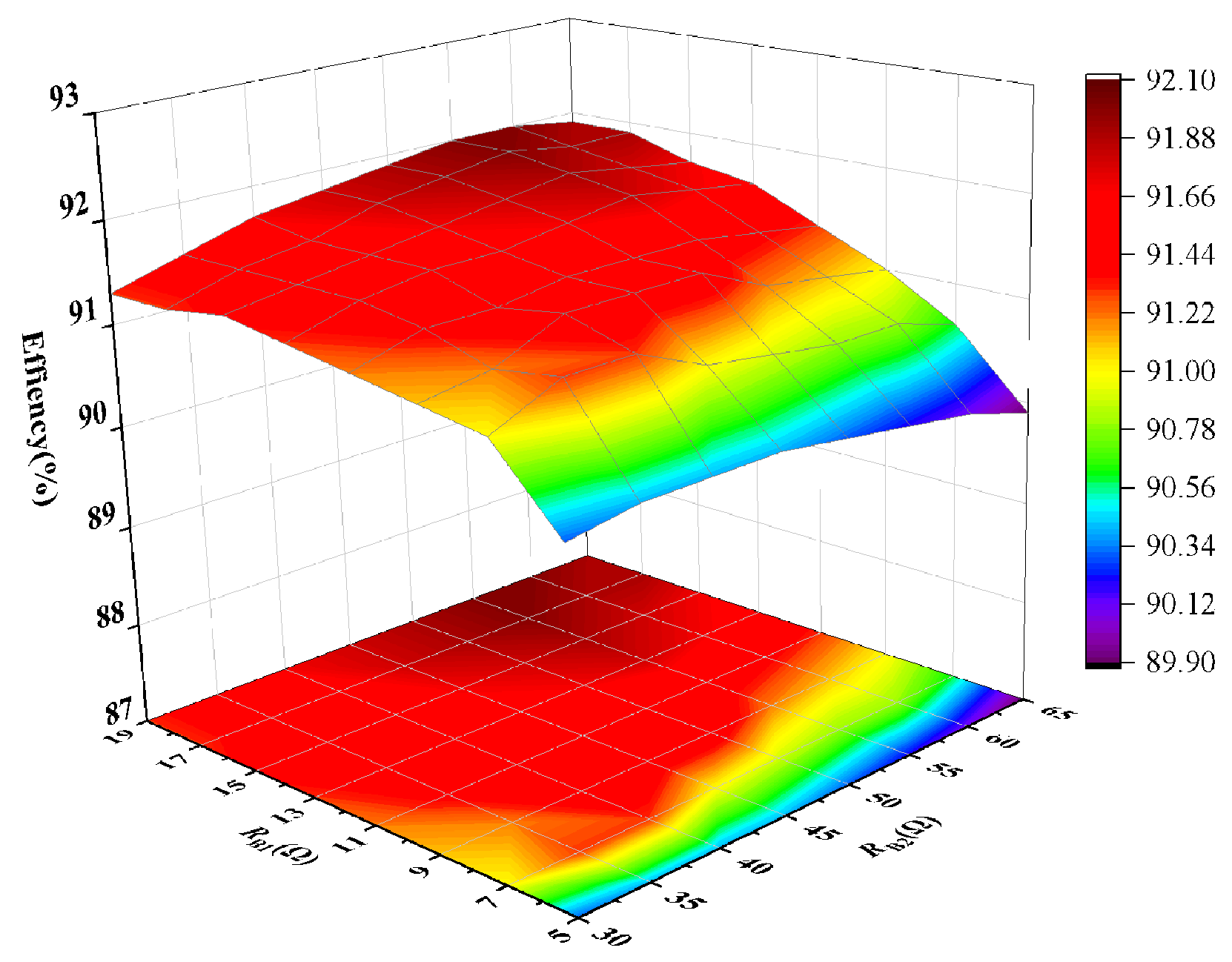
The overall efficiency surface of the system under different load conditions is shown in Figure 12. The proposed dual-output WPT system achieved a maximum efficiency of 92.1% under the conditions of an of 17 and an of 55 .
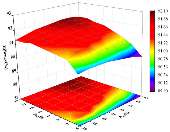
Figure 12.
The overall efficiency surface measured under different load conditions.
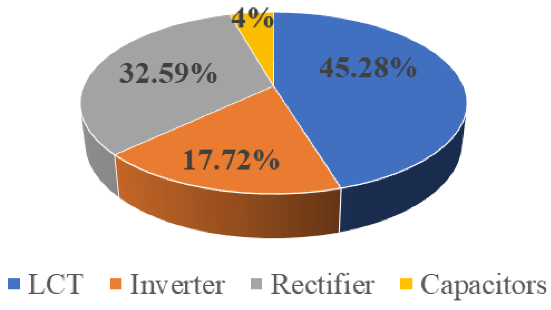
Same as the method in [28,29], the contribution of loss by each system’s component is obtained from the measured respective internal resistances and the measured resonant currents flowing through them. The resonant currents can be measured by an oscilloscope. The total power loss of the proposed system mainly includes the LCT loss, the compensation capacitors loss, the inverter loss, and the rectifier loss. Figure 13 shows that the losses generated by the two rectifiers and the magnetic coupler make up the vast majority of the total losses, with the rectifiers accounting for 32.59% and the magnetic coupler accounting for 45.28%. Using coils with high-quality factors can further cut down the losses of the magnetic coupler.

Figure 13.
Power loss distribution of each system component measured under aligned conditions with a load resistor of 17 and a load resistor of 55 .
For the purpose of further illustrating the merits of the dual-output WPT system proposed in this paper, the results of this study in comparison with previous similar studies are shown in Table 4 and summarized as follows:
Table 4.
The results of this study in comparison with previous similar studies.
(1) In the dual-output WPT system proposed in this paper, the coupling interference is eliminated by rationally designing the magnetic coupler. Compared with [15,20,21,22,23], it does not require complex control strategies and is more suitable for practical applications.
(2) In this paper, a dual-output WPT system is proposed, characterized by its simple structure and fewer compensation components, which reduce the system’s weight and cost and provide greater benefits compared to [19,22,23,25].
(3) In the proposed system, the relay coil and the first receiver coil are combined onto the ferrite plate on the first receiving side. Compared with [15,19,20,21,22,23], it effectively improves the space utilization of the system and makes the system more compact.
6. Conclusions
In this paper, a dual-output WPT system with a special decoupling design is proposed. This system has the ability to realize CC and CV dual outputs that are not affected by a load under ZPA conditions. The proposed magnetic coupler can achieve natural decoupling between the DD coil and the Q coil, which can eliminate the influence of cross-coupling. At the same time, the relay coil and the first receiver coil are combined onto the ferrite plate on the first receiving side, which greatly enhances the space utilization of the system. Compared with the traditional dual-output system, the proposed system has the characteristics of fewer compensation components, a compact design, elimination of cross-coupling interference, and simple control. Therefore, the system can be suited for various practical scenarios including electric vehicles and medical devices.
Author Contributions
Conceptualization, L.Y. (Le Yu) and Y.L.; methodology, Y.L.; software, Y.L.; validation, L.Y. (Le Yu), Y.L., L.Y. (Lin Yang), and X.Z.; formal analysis, L.Y. (Le Yu) and C.C.; investigation, L.Y. (Lin Yang); resources, L.Y. (Lin Yang); data curation, Y.L.; writing—original draft preparation, Y.L.; writing—review and editing, Y.L.; visualization, X.Z.; supervision, G.Y.; project administration, L.Y. (Lin Yang); funding acquisition, L.Y. (Lin Yang). All authors have read and agreed to the published version of the manuscript.
Funding
This research was funded by “Harbin manufacturing science and technology innovation talent project 2022HBRCCG006”; “Natural Science Foundation of Heilongjiang Province, under Grant LH2024E094”; “Natural Science Foundation of Hunan Province (NO. 2024JJ7186)”; and “Key Project of Hunan Provincial Department of Education (NO. 24A0589)”.
Institutional Review Board Statement
Not applicable.
Informed Consent Statement
Not applicable.
Data Availability Statement
The original contributions presented in this study are included in the article. Further inquiries can be directed to the corresponding author(s).
Conflicts of Interest
The authors declare no conflicts of interest.
References
- Wang, Q.; Li, Z.; Yang, B.; Lu, Y.; Mai, R.; He, Z.; Chen, Y. Inductive Power Transfer System with Constant Current-Constant Voltage Charging Tolerating Misalignment Based on Multi-Objective Optimization for Compensation Topology. IEEE Trans. Power Electron. 2025, 40, 4581–4591. [Google Scholar] [CrossRef]
- Jia, Y.; Zhao, L.; Wang, Z.; Tang, C.; Chen, F.; Feng, H. Integrated LCC-LCC Topology for WPT System with CC Output Regarding Air Gap and Load Variations. IEEE Trans. Power Electron. 2024, 39, 11904–11915. [Google Scholar] [CrossRef]
- Lillholm, M.-B.; Dou, Y.; Chen, X.; Zhang, Z. Analysis and Design of 10-MHz Capacitive Power Transfer with Multiple Independent Outputs for Low-Power Portable Devices. IEEE J. Emerg. Sel. Top. Power Electron. 2022, 10, 149–159. [Google Scholar] [CrossRef]
- Chen, Y.; Yang, N.; Li, Q.; He, Z.; Mai, R. New parameter tuning method for LCC/LCC compensated IPT system with constant voltage output based on LC resonance principles. IET Power Electron. 2019, 12, 2466–2474. [Google Scholar] [CrossRef]
- Diekhans, T.; De, D. A dual-side controlled inductive power transfer system optimized for large coupling factor variations and partial load. IEEE Trans. Power Electron. 2015, 30, 6320–6328. [Google Scholar] [CrossRef]
- Wang, S.; Liu, Y.; Wang, X. Resonant Converter for Battery Charging Applications with CC/CV Output Profiles. IEEE Access 2020, 8, 54879–54886. [Google Scholar] [CrossRef]
- Qu, X.; Zhang, W.; Wong, S.-C.; Tse, C.-K. Design of a Current-Source-Output Inductive Power Transfer LED Lighting System. IEEE Trans. Instrum. Meas. 2015, 3, 306–314. [Google Scholar]
- Li, Y.; Hu, J.; Li, X.; Wang, H.; Cheng, K.W.E. Cost-effective and compact multistring LED driver based on a three-coil wireless power transfer system. IEEE Trans. Power Electron. 2019, 34, 7156–7160. [Google Scholar] [CrossRef]
- Li, Y.; Hu, J.; Li, X.; Chen, F.; Xu, Q.; Mai, R.; He, Z. Analysis, Design, and Experimental Verification of a Mixed High-Order Compensations-Based WPT System with Constant Current Outputs for Driving Multistring LEDs. IEEE Trans. Ind. Electron. 2020, 67, 203–213. [Google Scholar] [CrossRef]
- Arnitz, D.; Reynolds, M. MIMO wireless power transfer for mobile devices. IEEE Pervasive Comput. 2016, 15, 36–44. [Google Scholar] [CrossRef]
- Mai, R.; Li, H.; Liu, Y.; Zhou, K.; Fu, L.; He, Z. A Three-Phase Dynamic Wireless Charging System with Constant Output Voltage. Energies 2018, 11, 45. [Google Scholar] [CrossRef]
- Jonah, O.; Georgakopoulos, S.; Tentzeris, M.M. Orientation insensitive power transfer by magnetic resonance for mobile devices. In Proceedings of the 2013 IEEE Wireless Power Transfer (WPT), Perugia, Italy, 15–16 May 2013; pp. 5–8. [Google Scholar]
- Hossain, A.; Darvish, P.; Mekhilef, S.; Tey, K.S.; Tong, C.W. A new coil structure of dual transmitters and dual receivers with integrated decoupling coils for increasing power transfer and misalignment tolerance of wireless EV charging system. IEEE Trans. Ind. Electron. 2021, 69, 7869–7878. [Google Scholar] [CrossRef]
- Wang, H.; Cheng, K. Analysis, design, and validation of a decoupled double-receiver wireless power transfer system with constant voltage outputs for industrial power supplies. IEEE Trans. Ind. Inform. 2022, 19, 362–370. [Google Scholar] [CrossRef]
- Wang, X.; Leng, M.; Zhang, X.; Tian, Q.; Zhou, X.; Guo, B.; Ma, H. Multioutput Wireless Charger for Drone Swarms with Reduced Switch Requirements and Independent Regulation Capability. IEEE Trans. Ind. Electron. 2024, 71, 4883–4895. [Google Scholar] [CrossRef]
- Casanova, J.; Low, Z.; Lin, J. A Loosely Coupled Planar Wireless Power System for Multiple Receivers. IEEE Trans. Ind. Electron. 2009, 56, 3060–3068. [Google Scholar] [CrossRef]
- Song, K.; Yang, G.; Guo, Y.; Lan, Y.; Dong, S.; Jiang, J. Design of DD Coil with High Misalignment Tolerance and Low EMF Emissions for Wireless Electric Vehicle Charging Systems. IEEE Trans. Power Electron. 2020, 35, 9034–9045. [Google Scholar] [CrossRef]
- Campi, T.; Cruciani, S.; Feliziani, M. Magnetic shielding of wireless power transfer systems. In Proceedings of the 2014 International Symposium on Electromagnetic Compatibility, Tokyo, Japan, 12–16 May 2014; pp. 422–425. [Google Scholar]
- Mai, R.; Luo, Y.; Yang, B.; Song, Y.; Liu, S.; He, Z. Decoupling Circuit for Automated Guided Vehicles IPT Charging Systems with Dual Receivers. IEEE Trans. Power Electron. 2020, 35, 6652–6657. [Google Scholar] [CrossRef]
- Wang, X.; Xu, J.; Ma, H.; Zhang, Y. A Reconstructed S-LCC Topology with Dual-Type Outputs for Inductive Power Transfer Systems. IEEE Trans. Power Electron. 2020, 35, 12606–12611. [Google Scholar] [CrossRef]
- Zhong, W.; Hui, S.Y.R. Auxiliary Circuits for Power Flow Control in Multifrequency Wireless Power Transfer Systems with Multiple Receivers. IEEE Trans. Power Electron. 2014, 30, 5902–5910. [Google Scholar] [CrossRef]
- Gong, Y.; Zhang, Z.; Chang, S. Single-Transmitter-Controlled Multiple-Channel Constant Current Outputs for In-Flight Wireless Charging of Drones. IEEE Trans. Ind. Electron. 2024, 71, 3606–3616. [Google Scholar] [CrossRef]
- Qi, C.; Huang, S.; Chen, X.; Wang, P. Multifrequency Modulation to Achieve an Individual and Continuous Power Distribution for Simultaneous MR-WPT System with an Inverter. IEEE Trans. Power Electron. 2021, 36, 12440–12455. [Google Scholar] [CrossRef]
- Pratik, U.; Varghese, B.J.; Azad, A.; Pantic, Z. Optimum Design of Decoupled Concentric Coils for Operation in Double-Receiver Wireless Power Transfer Systems. IEEE J. Emerg. Sel. Top. Power Electron. 2019, 7, 1982–1998. [Google Scholar] [CrossRef]
- Yang, L.; Dong, K.; Wang, Y.; Cai, C. Analysis and Design of a Dual-Receiver WPT System with Constant Current and Constant Voltage Dual-Type Outputs. IEEE Trans. Transp. Electrif. 2024, 11, 4060–4069. [Google Scholar] [CrossRef]
- Zhang, Y.; Yan, Z.; Liang, Z.; Li, S.; Mi, C.C. A high-power wireless charging system using LCL-N topology to achieve a compact and low-cost receiver. IEEE Trans. Power Electron. 2019, 35, 131–137. [Google Scholar] [CrossRef]
- Peng, C.; Chen, Z.; Liu, Z.; Wang, J.; Liang, J.; Li, C.; Tao, S.; Li, J. On the Load-Independence of a Multi-Receiver Wireless Power Transfer System. IEEE Microw. Wirel. Components Lett. 2019, 29, 563–565. [Google Scholar] [CrossRef]
- Vu, V.; Tran, D.; Choi, W. Implementation of the constant current and constant voltage charge of inductive power transfer systems with the double-sided LCC compensation topology for electric vehicle battery charge applications. IEEE Trans. Power Electron. 2017, 33, 7398–7410. [Google Scholar] [CrossRef]
- Niu, S.; Yu, H.; Niu, S.; Jian, L. Power loss analysis and thermal assessment on wireless electric vehicle charging technology: The over-temperature risk of ground assembly needs attention. Appl. Energy 2020, 275, 115344. [Google Scholar] [CrossRef]


Disclaimer/Publisher’s Note: The statements, opinions and data contained in all publications are solely those of the individual author(s) and contributor(s) and not of MDPI and/or the editor(s). MDPI and/or the editor(s) disclaim responsibility for any injury to people or property resulting from any ideas, methods, instructions or products referred to in the content. |
© 2025 by the authors. Licensee MDPI, Basel, Switzerland. This article is an open access article distributed under the terms and conditions of the Creative Commons Attribution (CC BY) license (https://creativecommons.org/licenses/by/4.0/).