1. Introduction
One of the key components in the future Internet of Things (IOT) era is sensors. Chemical sensors—for example, organic explosive related chemical sensors—will play an important role in environmental monitoring and security surveillance. Many types of electrical transducer platforms utilizing organic semiconductors have been proposed and engineered to detect chemical compounds. The majority of chemical sensors are built on conventional platforms of resistors [
1,
2,
3,
4] and field-effect transistors [
5,
6,
7,
8,
9]. The indication of chemical detection of these devices is mainly the change in resistance. In addition, some electrical transducers are based on capacitor [
10,
11] and diode [
12,
13] platforms. Overall, their transduction principles rely on the modulation of the organic layers electronic properties due to interactions with chemical analytes. As a result, a measurable change in device output is subsequently presented. However, it is really a challenge to build and operate sensors and devices comprised of organic semiconductors. This is because unexpected photochemical and oxidative reactions can occur in the organic layer during the electrical measurement, causing adverse effects on device performance [
14]. For example, damage due to the penetration of oxygen and water [
15] into the organic layer can cause degradation in mobility and threshold voltage [
16], leading to poor performance and instability. Some of these types of damage in the organic layers are irreversible.
In this work, we report a new type of chemical sensors consisting of a single layer organic photovoltaics to detect explosive related compounds such as nitroaromatics. Usually, single-layer organic photovoltaics have low efficiency due to insufficient charge separation and collection. The detection mechanism described within this work relies on the creation of a more favorable energy transfer, whereas an electron accepting compound is present. In general, the transduction mechanism for sensing such compounds relies on electron transfer from a higher energy donor to a lower energy acceptor. This type of energy transfer is hindered by the lack of an accepting layer in single layer photovoltaics. The proposed device relies on the formation of a temporary heterojunction introduced by an electron accepting compound in the gas/vapor phase, thereby enhancing the sensing efficiency.
2. Device Fabrication and Characterization Methods
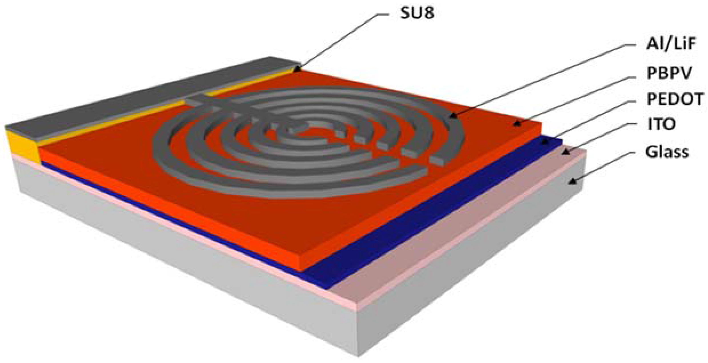
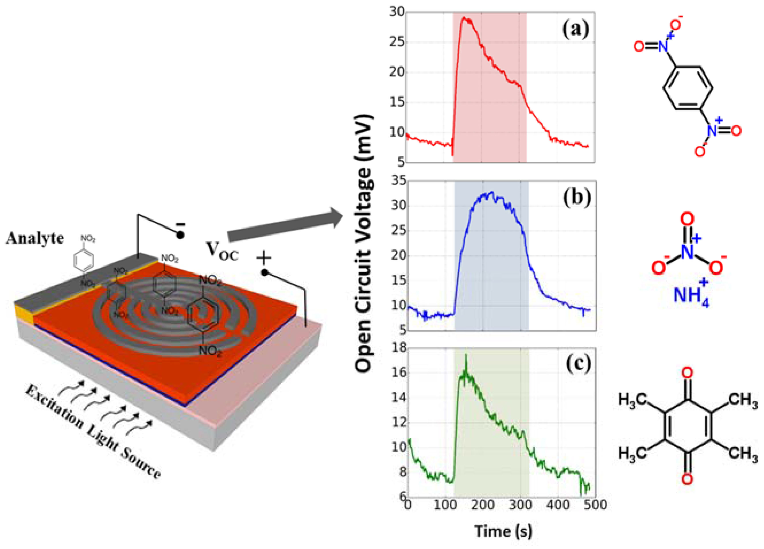
The sensor was fabricated on indium tin oxide (ITO) coated glass (Sigma-Aldrich, St. Louis, MO, USA). The device structure is shown in
Figure 1. Prior to any cleaning, the ITO substrate was coated with SU8 photoresist (Microchem, Westborough, MA, USA). Standard photolithography was used to define an electrically insulating contact pad. This was followed by a hard bake for 5 min at 150 °C. The insulating pad helps to reduce the risk of short circuit between the cathode and the ITO anode when an external contact is applied during testing. The ITO substrate was then cleaned by successive soaking in acetone, methanol, isopropyl alcohol, and deionized water then followed by nitrogen drying. The cleaned substrate was then treated with oxygen plasma at a power of 60 W for 4 min in order to promote a more hydrophilic surface for subsequent water based poly(3,4-ethylenedioxythiophene) poly (styrenesulfonate) (PEDOT) deposition. PEDOT was filtered through a 45 µm filter and spin casted on the sample at 3000 rpm for 30 s, yielding a layer approximately 50 nm thick. The PEDOT layer was then baked at 120 °C for 5 min on a hot plate to remove excess water contained within the film. A Poly[2,5-bisoctyloxy)-1,4-phenylenevinylene] (PBPV) (Sigma-Aldrich, St. Louis, MO, USA) solution was prepared in chloroform at a concentration of 3.5 mg/mL then spin casted on the PEDOT layer at 3000 rpm for 30 s. The sample was then baked again at 120 °C for 5 min to remove excess solvent. The remaining fabrication steps involve the deposition of the cathode layers using thermal evaporation and the defining of the deposition area by using a shadow mask. The shadow mask was designed to have a set of five concentric semi-circles with decreasing diameters. Each semi-circle had a thickness of ~1.3 mm and the diameters in a descending order were 24.5, 19.5, 14.5, 9.5, and 4.5 mm. Lithium fluoride (Sigma-Aldrich, St. Louis, MO, USA) was evaporated at a rate of 8 nm/min with a final layer thickness of 0.5 nm, followed by aluminum (Al, Kurt Lesker, Jefferson Hills, PA, USA) at a rate of 12.3 nm/min with a final thickness of 100 nm, as measured with a crystal rate monitor. The thickness of the spin cast films was measured with a Veeco profilometer (Veeco, Plainview, TX, USA) to be approximately 600 nm.
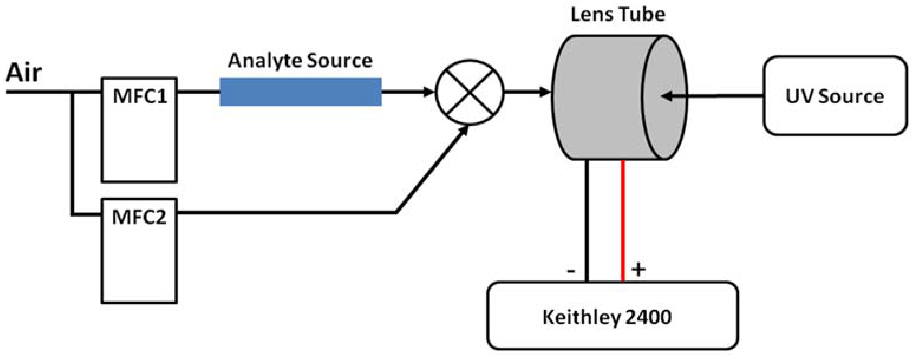
Figure 2 shows the device measurement setup, containing four key components. (i) Two mass flow controllers (MFC1 and MFC2) (MKS Instruments, Andover, MA, USA) provide precise air flow to the analyte source and a dilution line for varying the concentration. In this work, the testing analytes include 1,4-dinitrobenzene C
6H
4(NO
2)
2 (1,4-DNB), ammonium nitrate (NH
4NO
3), and duroquinone (C
10H
12O
2); (ii) An enclosed optical lens tube which contains the sensor is connected with both a gas inlet port allowing the gas analyte to impinge on the device surface and a fiber optic couple on the opposite side to illuminate the device through its glass substrate; (iii) A light source containing 365 nm and 470 nm light emitting diodes, the ultra violet (UV) light source, is coupled to the lens tube and operated to provide approximately 1 mW illumination power; (iv) A Keithley 2400 source meter (Tektronix, Beaverton, OR, USA) controlled through Labview (National Instruments, Austin, TX, USA) is used to measure the open circuit voltage. Once the device was optically excited with the UV light source, a constant flow of air was introduced in order to establish a baseline, stabilization open-circuit voltage. After a baseline period, the device was exposed to the saturated analyte vapor at a specified dilution while maintaining a constant flow rate to avoid pressure induced changes.
3. Design of Organic Photovoltaic Sensors
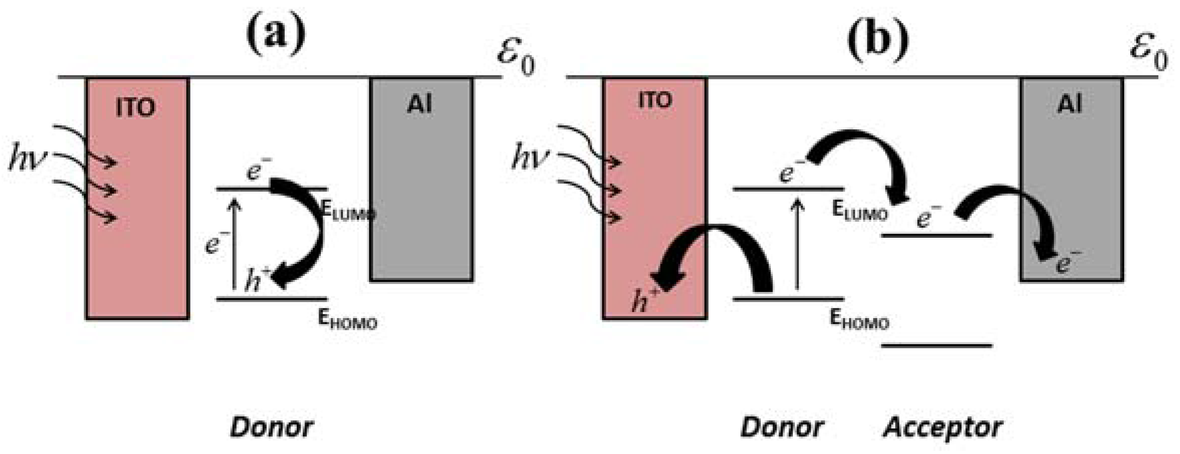
Single-layer organic photovoltaic cells generally consist of an organic layer sandwiched between a transparent anode and low-work-function cathode. Upon absorption of a photon, an electron in the organic semiconductor is excited from the highest occupied molecular orbital (HOMO) to the lowest unoccupied molecular orbital (LUMO). Due to the low dielectric constant and localized electron and hole wavefunctions in organic semiconductors, strong Coulombic attraction exists between the electron–hole pair. The resulting bound electron–hole pair is called an exciton [
17,
18]. Photovolatic cells made of a single organic layer and two electrodes tend to be inefficient. There are two possible reasons: (1) the excitons are usually not split by the built-in electric field which arises from the differences in the electrode work functions [
19]; or (2) a large energy barrier exists at the cathode, preventing charge transfer. The illustration in
Figure 3a shows the operation of a single layer organic photovoltaic cell which, in this case, utilizes an ITO anode and Al cathode. After the exciton is created, it has a diffusion lifetime which ends through a decay pathway. Possible decay pathways include radiative decay to its ground state, non-radiative decay to its ground state, trap states, or transfer to a collection electrode. In this case, recombination of the bound electron and hole occurs due to an unfavorable transfer to the cathode.
The efficiency of charge separation and collection can be enhanced by a heterojunction at the interface between the donor and acceptor (not the electrode contacts), which defines the properties of the device [
20]. A heterojunction consists of two different semiconductor materials with two different bandgaps. The LUMO level of the donor must be energetically higher than the acceptor LUMO in order to donate its electrons [
21]. When an exciton diffuses to the donor–acceptor interface, the energy level offset between the donor and acceptor induces an electron transfer across the interface [
22]. If an adequate energy offset exists, the exciton may be converted into a free electron and a free hole, resulting in electron–hole charge separation. Otherwise, the excited charge state will decay to a lower energy level or become captured by a recombination center. Therefore, the charges can now diffuse to their respective electrodes [
22].
Figure 3b illustrates increased charge collection when an electron acceptor is present, allowing a lower energy transfer path to the cathode.
As described above, an effective strategy for facilitating charge separation is to insert an electron acceptor material, whereas a heterojunction structure is formed. A heterojunction device containing two different materials can be either physically created during fabrication or temporarily formed upon exposure to the organic analytes. As shown in
Figure 3b, when a single layer photovoltaic is exposed to an electron accepting analyte, a temporary heterojunction can be formed, inducing an increase in charge collection which ultimately leads to a larger open-circuit voltage. The analyte to which the device is exposed should have a LUMO lower than that of the organic layer in order for a favorable charge transfer.
4. Results and Discussion
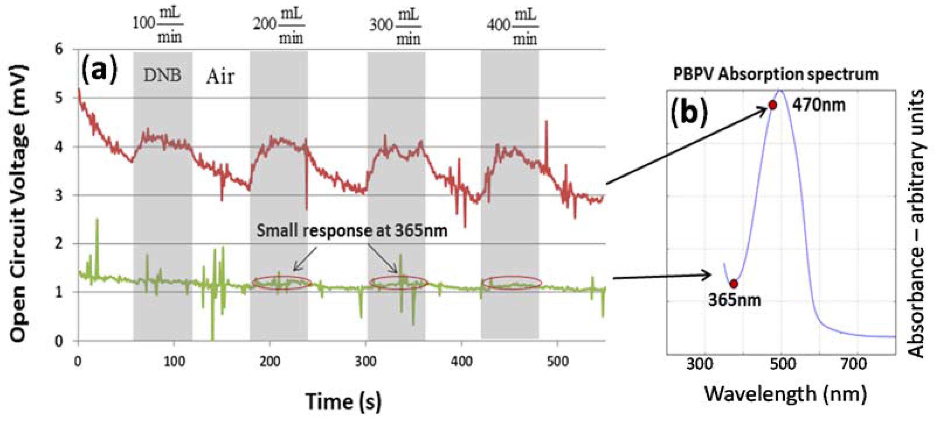
As shown in
Figure 4a), Ultra Violet—Visible Spectroscopy (UV–VIS) absorption spectrum measurements were performed on the PBPV organic thin film, indicating absorption peaks at approximately 500 nm with diminished absorption on each side at 400 nm and 560 nm. Electrical measurements were then performed to determine whether the open-circuit voltage increases while the device is exposed to 1,4-DNB. The devices were subjected to 60 second pulses of analyte, the 1,4-DNB vapor, at increasing concentrations (flow rates: 100, 200, 300, and 400 mL/min) with 60 s periods of pure air flow after each pulse. 1,4-DNB flow rates represent 25%, 50%, 75%, and 100% saturated vapor pressure which corresponds to 196.4, 392.8, 589.1, and 785.5 ppb. The pure air flow is to clean the analyte in the sample tube and recover the open-circuit voltage. The total flow rate was held constant through each experiment to avoid any pressure-induced change to the measured voltage. A 365 nm light source was used as it falls within the absorption spectrum of PBPV film. Since the absorbance at this wavelength is low, a small change or no response in open-circuit voltage is expected for this case. Indeed, as shown in
Figure 4b, with 365 nm excitation the measured voltage showed a very small increase during 1,4-DNB exposure at 200, 300, and 400 mL/min flow rates. Such a small change is even less noticeable than the noise—it is hard to tell if the analyte flow is on or off.
In another experiment, a 470 nm light source was chosen as it lies at almost the peak absorption of the PBPV film. The voltage response indicates that while the device is excited at this wavelength and exposed to 1,4-DNB, the measured voltage exhibits a significant increase (more than 33%) which returns to nearly its baseline value upon removal of the analyte. Also, for the increasing flow rate of 1,4-DNB, the magnitude of the open-circuit voltage response is relatively the same and does not show a concentration dependence. This could be an indicator that the magnitude of the response is dictated by the energy level difference between the organic donating layer and the analyte. If this was the case, such a chemical sensor will have a different response to different chemicals. This assumption will be further tested and verified in the following measurements.
As shown in
Figure 5, a 470 nm light source was used to further test 1,4-DNB, duroquinone (DQ), and ammonium nitrate (AN), which are all electron-acceptor analytes. 1,4-DNB is chemically similar to trinitrotoluene (TNT), a commonly used explosive, but has a higher vapor pressure and is easier to obtain in a laboratory than TNT. DQ is not considered an explosive analyte but is a strong electron acceptor. The AN analyte has been a favorite material used in improvised explosive devices [
23] and is also an electron-acceptor analyte. However, AN has a very low vapor pressure, making it difficult to detect at room temperature. For each measurement, the saturated vapor of each analyte was used and an identical procedure is followed: (i) 120 s baseline period of 400 mL/min air flow; (ii) 120 s sample period of 400 mL/min analyte flow; and then (iii) 120 s recovery period of 400 mL/min air flow.
The results indicated that all three analytes produced an increase in the open-circuit voltage, which agrees with the consideration of their electron accepting nature. Among these three analytes, AN induced the largest increase in open-circuit voltage which is almost two times of that induced by DQ. Also, the response to AN vapor (
Figure 5b) has a longer rising time towards its peak response compared to the 1,4-DNB and DQ vapors. These differences in response voltages and times can be used to discriminate different organic chemical vapors which are chemically and structurally similar electron acceptors. To achieve a better chemical discrimination, a transient feature analysis with machine learning algorithms [
24,
25] can be applied on this new type of chemical sensors. This will be a future independent study.
In addition, we found that the open-circuit voltage reaches a maximum value and then decreases even when the analyte vapor is still flowing. This is really understandable. The analyte molecules are physically absorbed on the surface of PBPV thin films, making the charge transfer between them difficult. Also, the charge transfer among the analyte molecules is also not efficient. After the electron transferring out of the first layer of analyte molecules to the Al electrodes, electron charges are not compensated back to the analyte from the PBPV film, which disables the temporary heterojunction and decreases the open-circuit voltage after the maximum value. Nonetheless, the change of open-circuit voltage and the pattern of the response signal are sufficient for detection.
Moreover, such a chemical sensor design is not limited to PBPV film. More explosive-related chemicals can be detected and discriminated if organic thin films with varying energy levels are used in the sensors. Furthermore, an array of photovoltaic chemical sensors or sensor networks comprised of different organic thin films will be able to selectively, simultaneously detect a variety of explosive compounds or a mixture of chemical compounds.


