1. Introduction
The ultimate goal of an integrated circuits (IC) physical design electronic design automation (EDA) tool is to accomplish any physical implementation, with respect to functional design (no timing violations), and to honor all of the rules of physical design. In advanced technology nodes, from 16 nm all the way to 7 nm, the routing step becomes the most complicated task in the physical implementation of ICs. This is mainly due to the increase in design rules that must be respected, from one technological node to another. Practical examples of the new design rules in 7 nm technology node are the self-aligned double patterning (SADP) [
1] and aggressive end-of-line (EOL) rules. In a chip where performance is increasingly more than a simple requirement [
2], the perspective of delay due to unexpected physical design challenges is a frightening prospect. These new rules create an urgent need for new techniques that help to improve all quality aspects during physical IC implementation from floor-planning, placement, and clocktree synthesis (CTS) until the route [
3]. In this paper, we will take an important physical characteristic that comes with 7 nm SADP as an advantage to optimize wire delay by reducing the wire resistance. This comes from the fact that, due to the manufacturing process, the SADP layers, compared to No-SADP layers, have a high resistance. It is true that the previous tool versions already take the wire resistance into account during the wire promotion in the global route, but in this paper we are presenting an additional wire promotion that is SADP-based. A direct impact will be significant timing optimization without increasing cell area utilization. As a side effect, the consumed power by the wires will be reduced. As proof of concept, we will apply the proposed routing algorithm, using Nitro-SoC™, (2016.2, Mentor Graphics Corporation, Wilsonville, OR, USA, 2016), the Mentor Graphics’ physical design EDA tool, and a significant regression of 7 nm designs. The remainder of the paper is organized as follows: first, we present the global trends of delay sensitivity in advanced technology nodes, and we then try to explain the relationship between the wire delay and its resistance; next, we describe our solution as a new routing optimization method; timing is optimized via net delay reduction; finally, we present the experimental results on the selected regression, and a comparison study between baseline and the new method is also included.
2. Delay Sensitivity in Advanced Technology Nodes
In advanced technology nodes, the delay due to interconnect becomes more important than the delay in the gate. This is due to the increased delay sensitivity to the interconnect parasitic [
4].
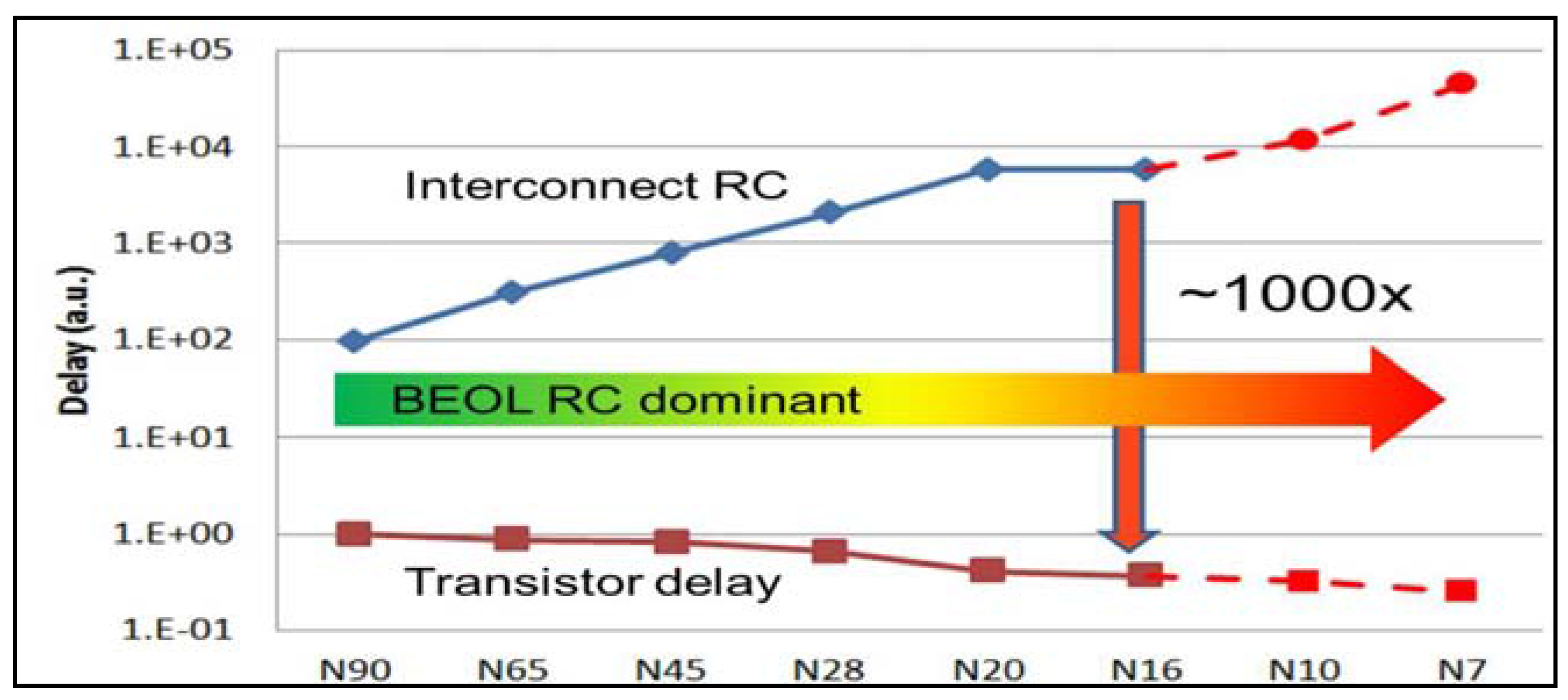
Figure 1 illustrates the escalating interconnect Resistance-Capacitance (RC) delay with nodes scaling.
With an approximately 10× growing gap for two process nodes, this escalating RC delay represents a significant part of the increase in gate density. This is due to the exponential increase in buffers and drivers counts, and a similar increase in “white” area kept for post-layout buffer insertion [
5]. As performance divergence between transistors and interconnects continues to increase, designs have become interconnect-limited [
6].
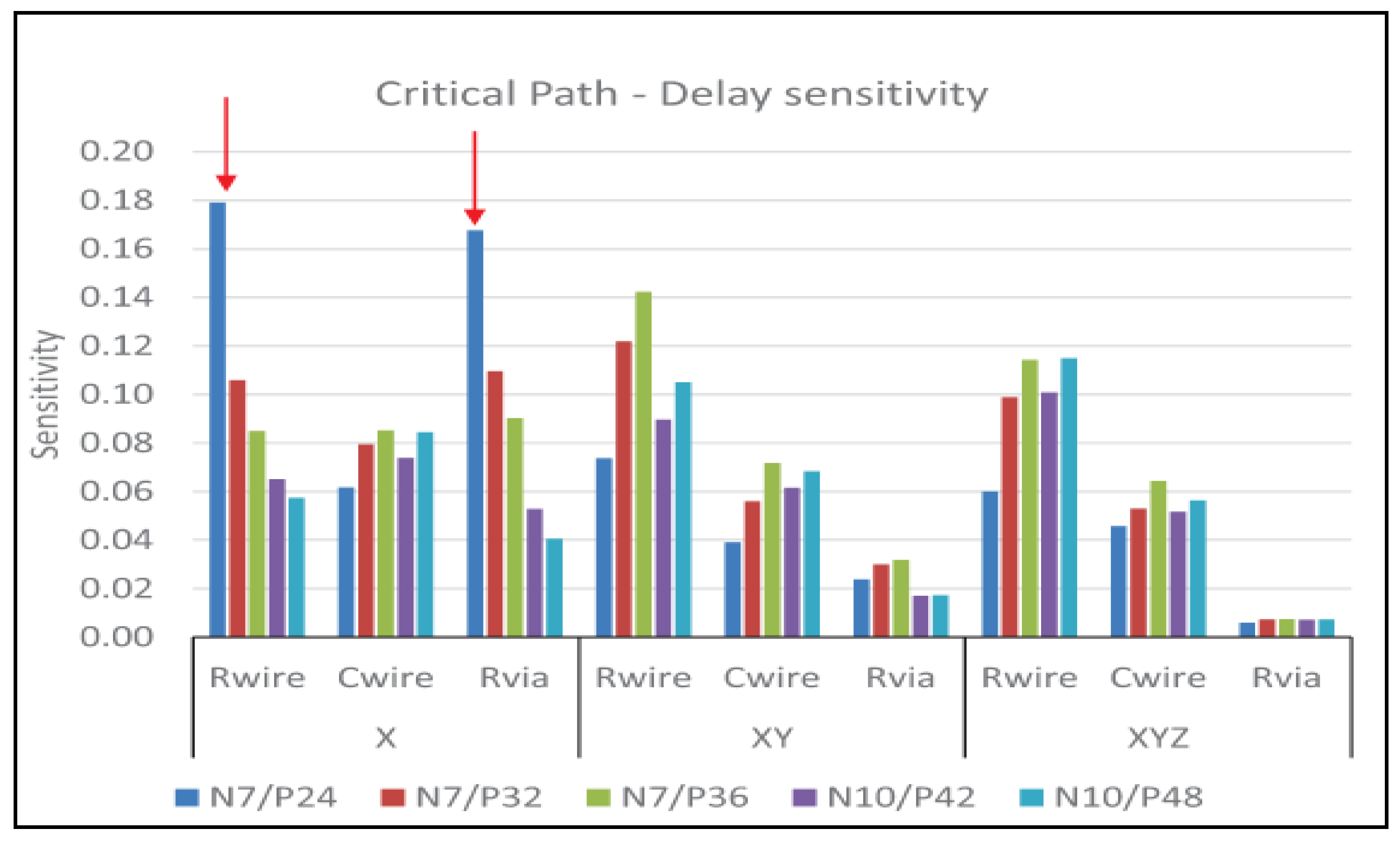
On the other hand, the delay is more sensitive to the wire resistance, more than it is to the wire capacitance [
7], as highlighted by
Figure 2.
Variables in the figure are defined as follows:
X represents local connections, i.e., short connections within cells. In general, the bottom layer is used.
XY represents intermediate connections between cells and cores/modules.
XYZ represents global connections, i.e., long wires.
To address the increasing complexities, physical designers need new routing techniques that can perform a full chip parasitic and timing optimization from placement to the route.
3. Wire Delay Model
The net delay is the time difference, between when a signal is first applied to the net, and when it reaches the other devices connected to that net. The net delay is a direct effect of the finite resistance and capacitance of that net; it is also known as the wire delay.
Wire delay is a function of
Rnet and
Cwire (
Cnet +
Cinput) [
8].
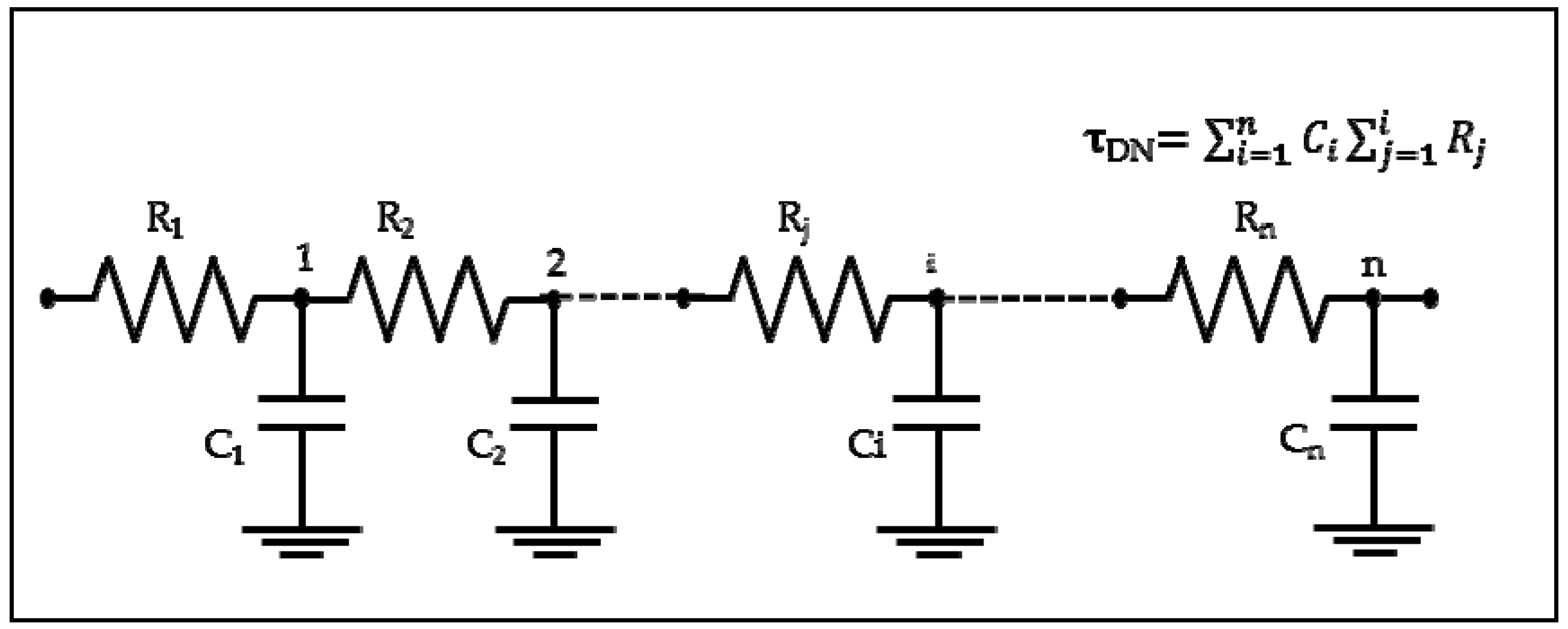
For the delay calculation in EDA tools, it is true that the delay is calculated using complex timing models such as Non-Linear Delay Model (NLDM) and Composite Current Source (CCS), but a simple model could be used for a rough estimation of delays like the “Elmore Delay formula” [
9] presented in
Figure 3. It can be concluded that reducing wire resistance implies wire delay (
τDN) reduction.
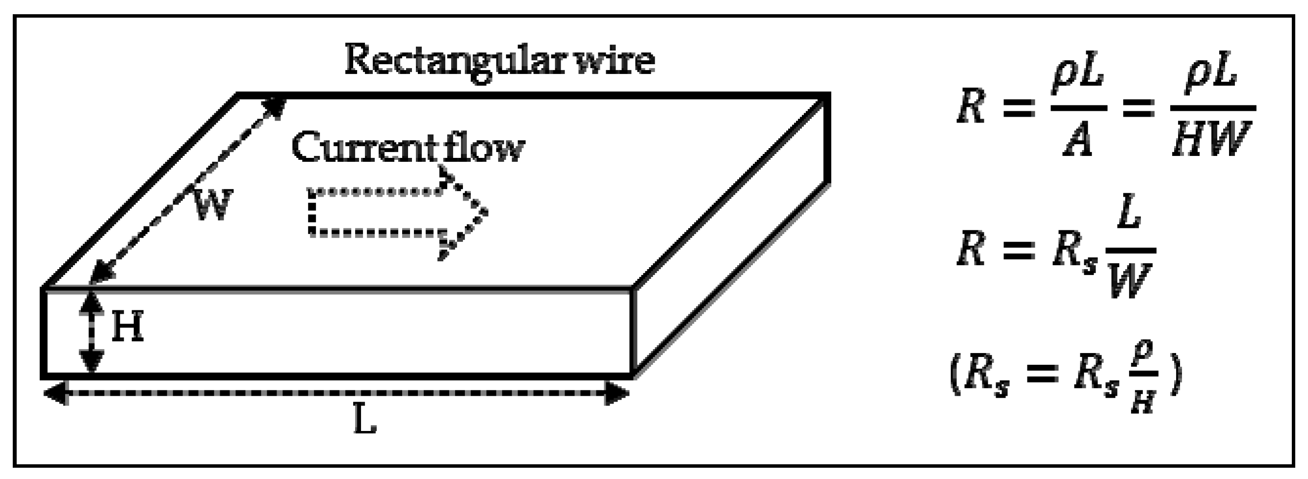
The resistance of a wire is proportional to its length L and inversely proportional to its cross-section A.
The resistance of a rectangular conductor is shown in
Figure 4. Where the constant
ρ is the resistivity of the material (in W-m) and H is a constant for a given technology [
9].
Rs is the sheet resistance of the material, having unit of W/sq (W-per-square). This expresses that the resistance of a square conductor is independent of its absolute size. To obtain the wire resistance, the sheet resistance is multiplied by its ratio (
L/
W), as shown in
Figure 4.
4. Wire Optimization to Reduce Net Delay
Traditional buffering and upsizing techniques to reduce interconnect delay are no longer as effective due to the area and power impact.
To minimize design costs and to better predict system performance, there is a need to use new techniques to optimize interconnects delay. In addition to what already exists in the EDA tool, we must take maximum advantage of the re-routing transforms during optimization for setup and hold instead of using size and buffer transforms.
In 7 nm technology, the spectrum of metal layer resistivity is large, from the top lesser resistive layers to the bottom SADP layers (M0, M1, M2, and M3).
In addition, wire etching induces great resistance differences based on metal density and spacing, with different values in congested areas versus sparse routing areas, different values for double-spacing around the wire or on only one side, and so on.
Table 1 shows the sheet resistance for each layer of 7 nm node technology used in our case study.
Metal 0 and Metal 1 are highly used by standard cells; the router mainly uses layers from Metal 2. From
Table 1, changing wire from Metal 2 to Metal 4 reduces its sheet resistance by 54% and by 46% from Metal 3 to Metal 4.
This is an interesting breakpoint, a potential reduction of the total wire resistance by more than 46%.
Our proposed routing optimization technique takes this technology propriety as a solution to reduce the critical net delay by re-routing the delay-critical nets with upper layers.
To limit any side effect that can affect routing quality and timing, the router is driven through non-default-rules (NDRs).
The main guidance is to use layers up to Metal 4 (No SADP layers) to route the critical nets. Nets that are not critical or less critical will be routed with all layers.
The wire optimization of timing critical nets using NDRs enables the optimization and routing engines to balance efficiently between the timing and congestion.
In parallel to the EDA tool software, there is a reference flow script that is “Tool Command Language” TCL-based to run each part of the Place & Route design flow step by step. It is made by a set of organized TCL scripts that cover different stages from placement to post-route. It includes all needed command and settings to implement a large variety of designs from low to high complexity. The used Nitro-SoC tool begins with floorplanning and placement, and then handles CTS, and routing. Signal integrity (SI) analysis and multi-corner/multi-mode (MCMM) analysis can be performed at any stage during the design flow. The Double Via Insertion, Double Patterning fixing, and Design For Manufacturing (DFM) optimizations are performed at the end of the flow [
3,
10].
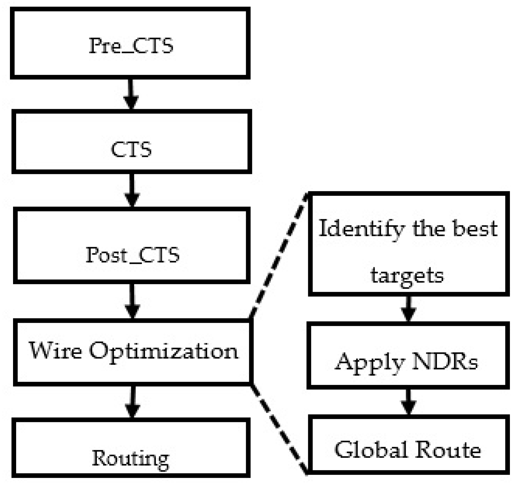
Our added solution is a set of TCL scripts that include Nitro-SoC basic commands. This solution is added exactly after the Post Clock Tree Synthesis (Post-CTS) within reference flow.
Figure 5 shows where we are adding the wire optimization inside the initial flow (baseline flow) and the section below gives more details for each step:
Create NDR rules that drive the global route to use Metal 4 and up.
Identify the best net targets for optimization, which is the most important step because a good optimization starts from good targets that result in a high delay reduction without any side regression. This is subdivided into four steps:
Start from a list of all nets that violate setup timing.
Select only nets with a delay up to a predefined threshold value. It is a procedure that helps in finding nets with a critical delay greater than the delay threshold. These nets are the right targets for our optimization.
Apply costing to remove nets that violate hold timing. A filtering is performed in order to keep only the nets that do not cause a violated hold timing path.
Remove nets that already have high No-SADP-layer usage. There will otherwise be no room for additional optimization.
Now we have a good list of target nets to re-route.
- 3.
Apply NDR to a sorted list of final target nets.
- 4.
Run the normal global route followed by a detail route.
Before executing a new global route, it is necessary to delete the old net’s global route. Then, perform a new one on the list of target nets.
5. Application and Results
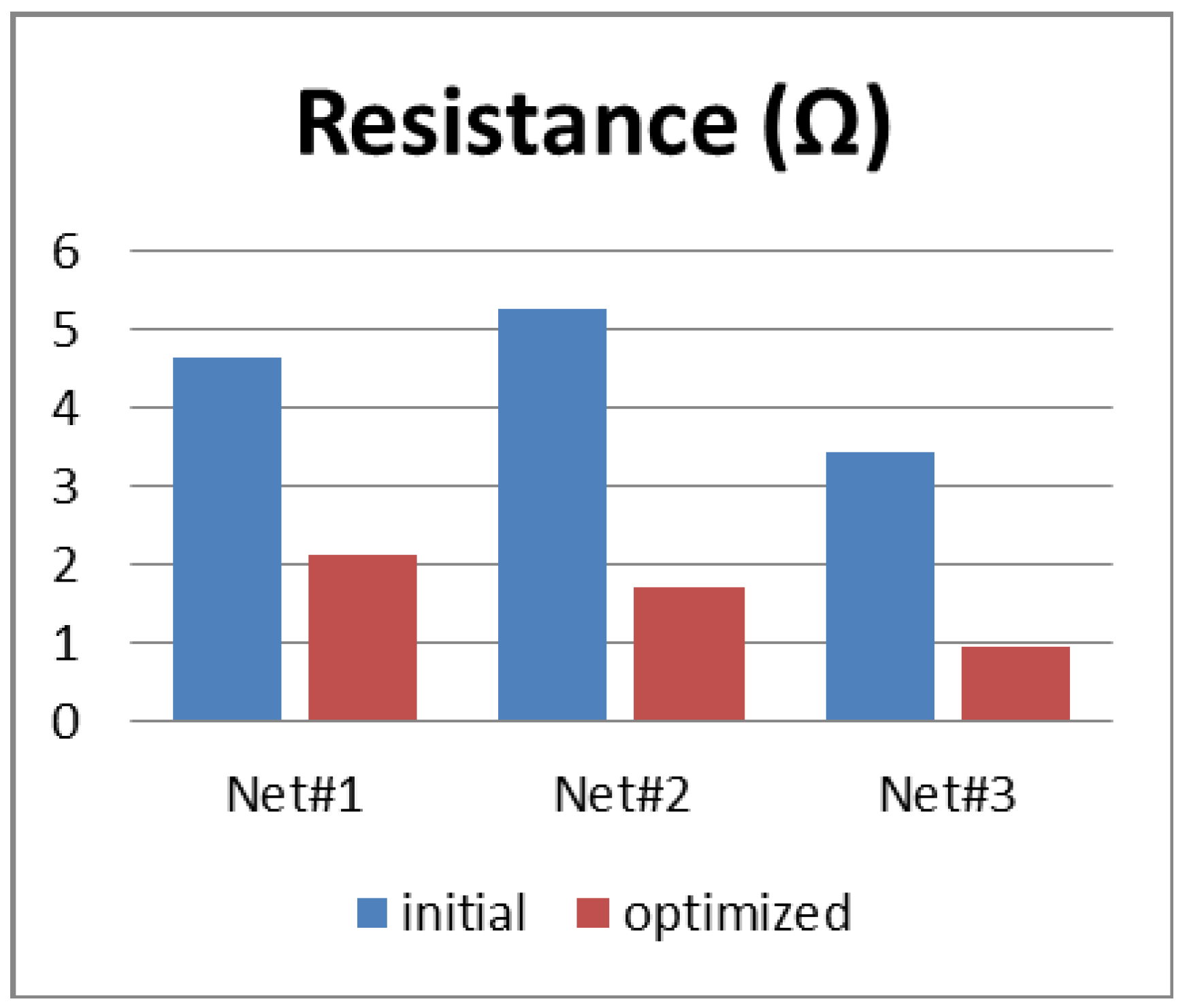
The first experiment was done on three critical nets belonging to the same timing path. Starting from a post-CTS database, we selected three critical nets with a delay higher than a predefined value (10 ps for our use case). We then applied our routing-optimization technique.
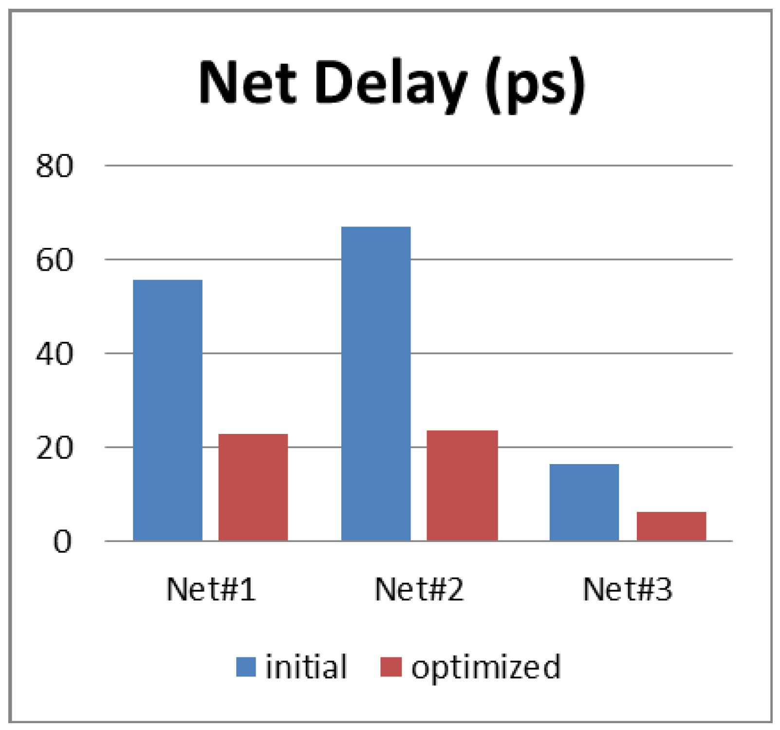
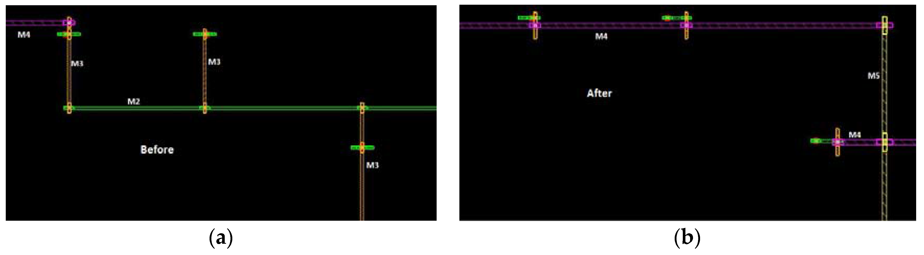
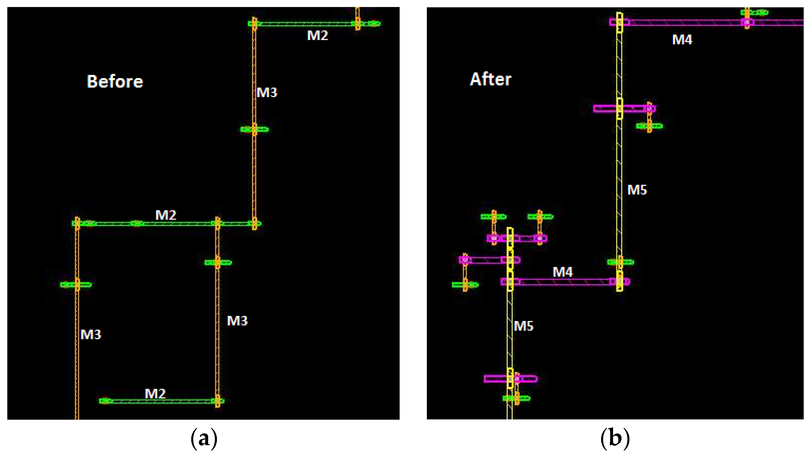
As shown in
Figure 6, the net resistance is significantly reduced. This result was expected since the router is now constructed to use Metal 4 and up. As a consequence, the net delay is globally reduced by 50%.
Figure 7 illustrates this result.
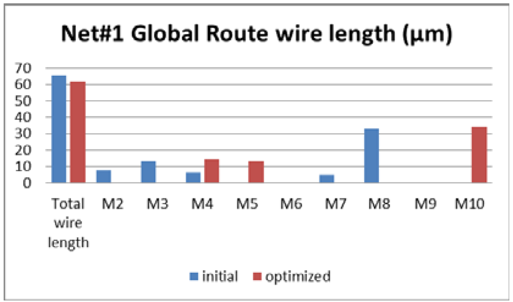
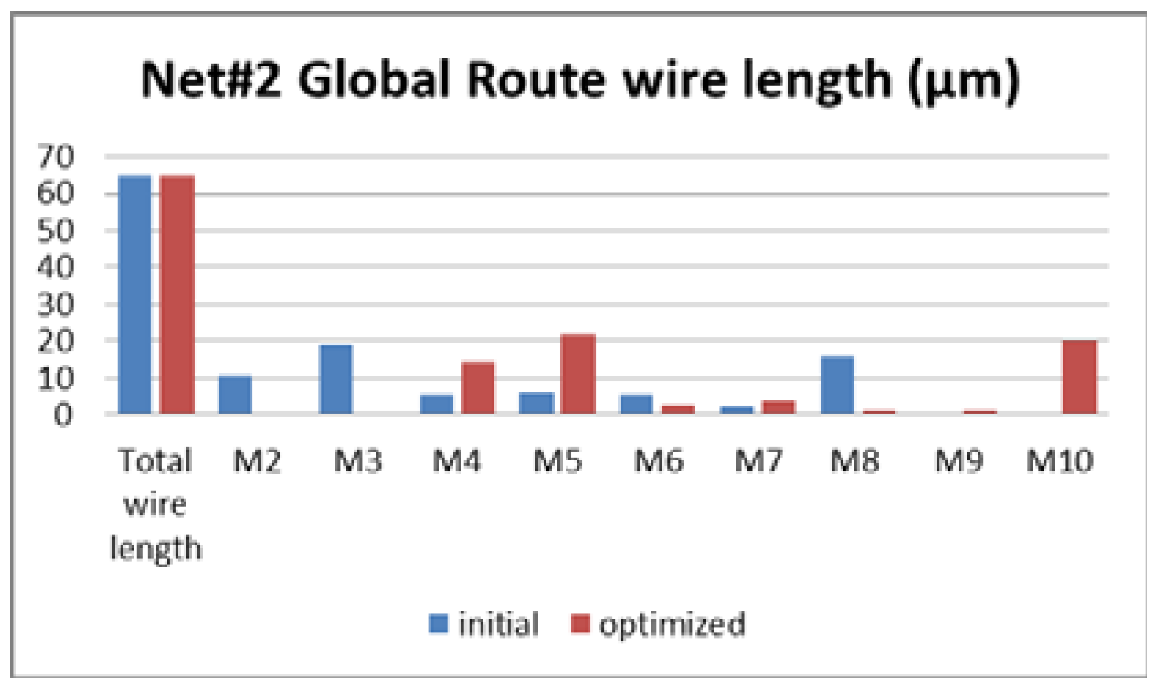
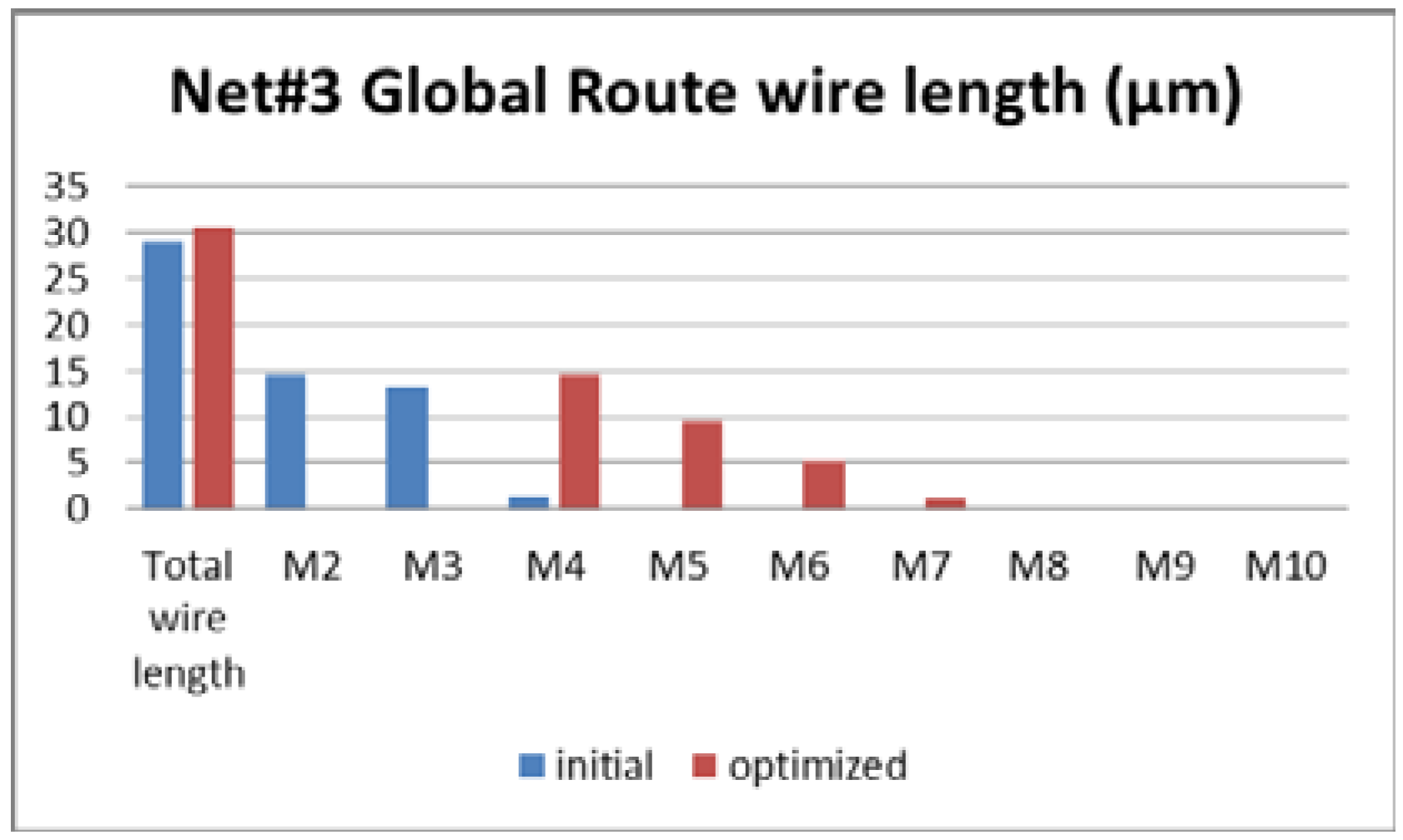
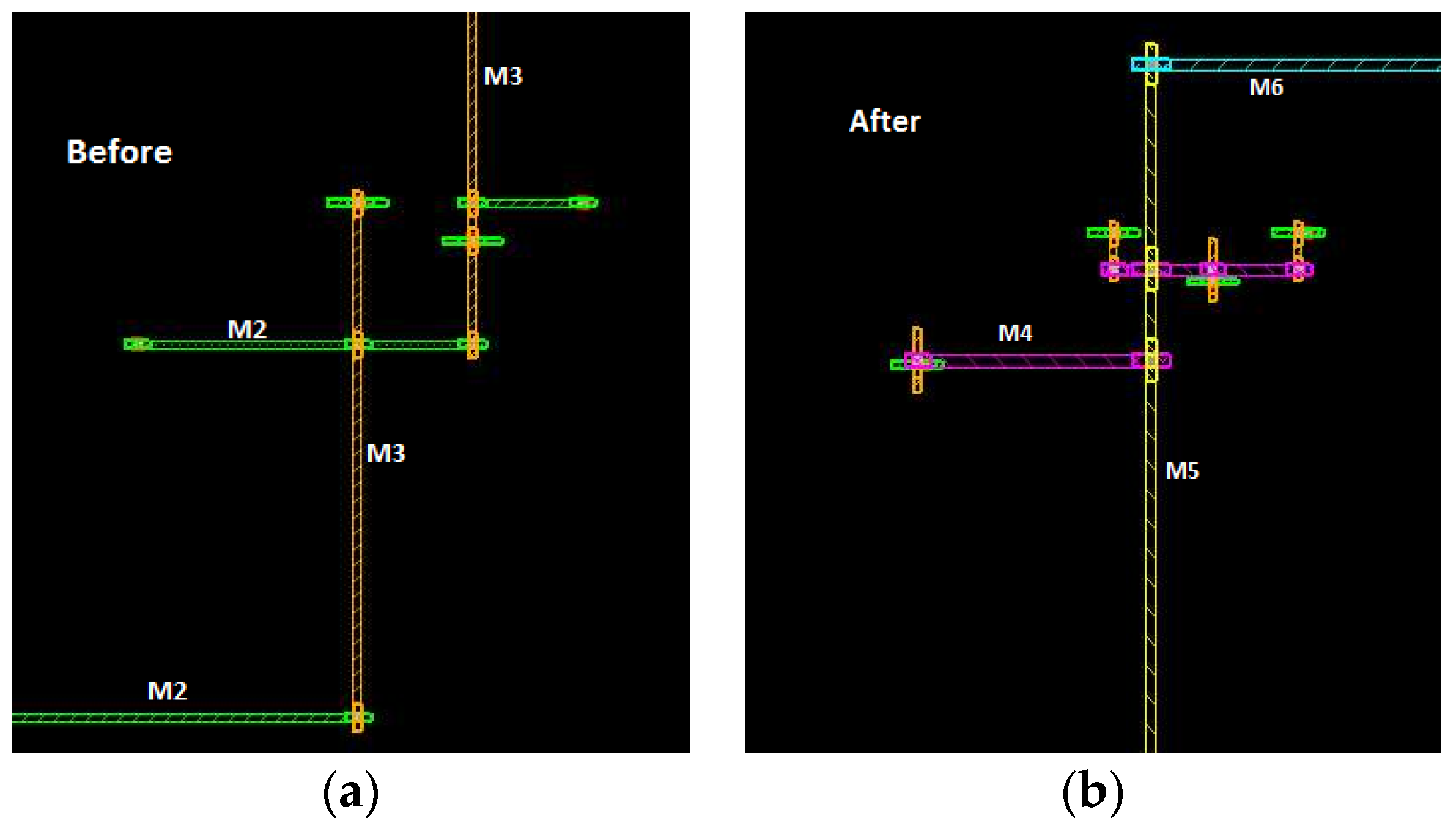
Figure 8,
Figure 9 and
Figure 10 show the metal layers distribution for Net#1, Net#2, and Net#3. It can be seen that, in the optimized routing, the used layers are up to Metal 4.
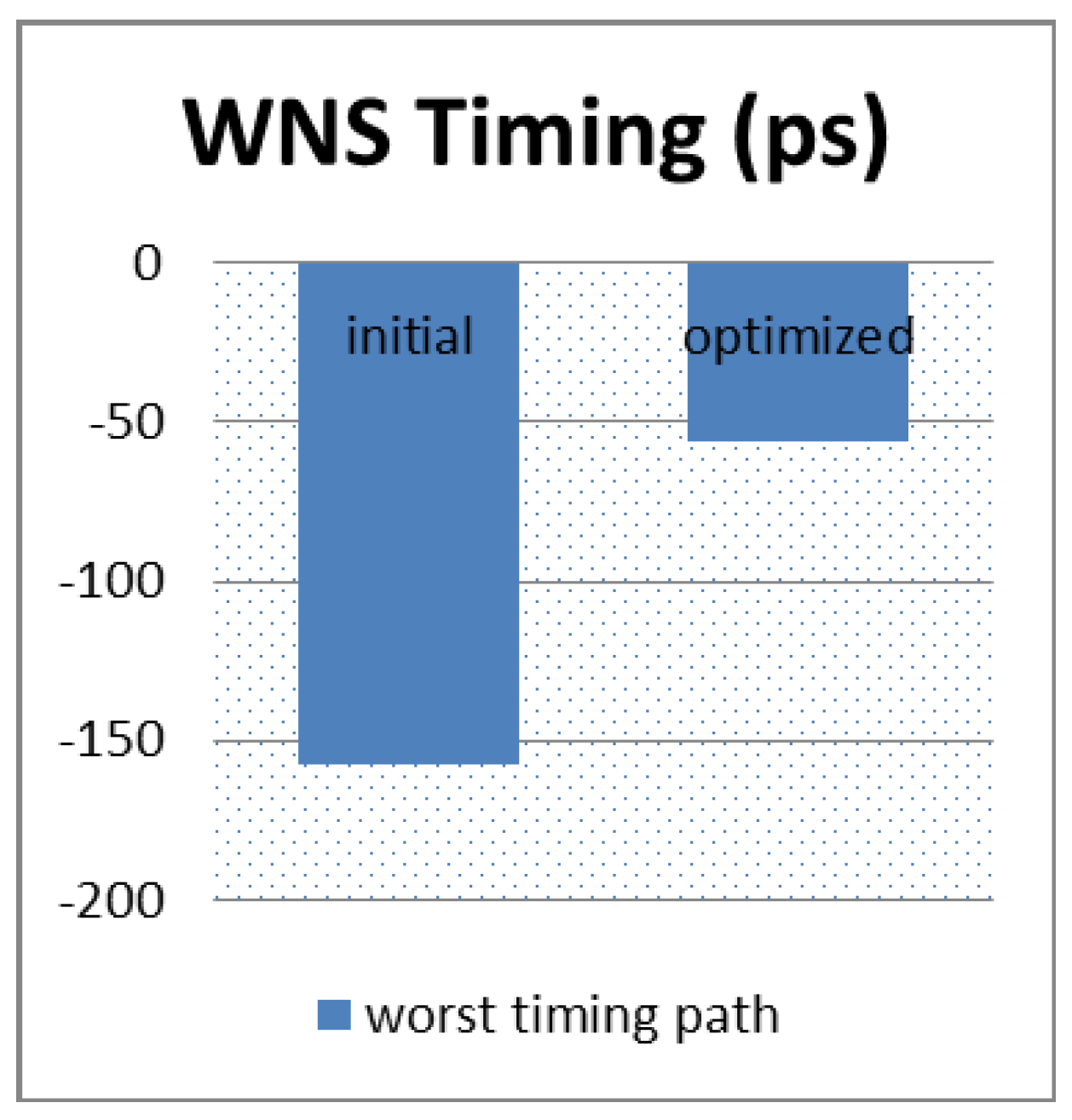
Figure 14 shows the expected benefit of the delay reduction; the worst negative slack (WNS) is optimized from −157.4 ps to −56.4 ps.
This first experiment on three critical nets demonstrates a WNS improvement up to ×2.8, with simple net re-routing. This presents an opportunity for physical designers to significantly reduce timing violations using routing optimization.
The complexity of resistance and capacitance variations makes it nearly impossible for the human mind to determine which combination of layers and via structures to use for a given net in order to obtain the best possible timing and routability.
However, at the same time, we can easily drive a place and route tool such as Nitro-SoC to take advantage of lesser resistivity of wires and vias. This can be achieved through NDRs.
In a real design, the task is more complicated because there is a need to take into account many constraints such as timing hold and setup, max transition, and route congestion. The best way to prove the benefits of a new route optimization methodology is to apply it on large design types. Thus, to go farther than just applying the wire optimization on a few nets of one design, we applied this new route optimization on several types of designs. This will be the aim of the second experiment.
All test cases designs are made with a full place and route flow starting from the floorplan, with the following conditions:
- -
N7-SADP technology node with stack layers [M0 … M12] is used;
- -
the starting databases are the same for the baseline and feature flow;
- -
the power grid is achieved using the M11 and M12 top layers, going through others layers to standard cells power ports.
Average area occupancy for each layer for both power and ground nets is distributed as presented in
Table 2.
- -
clock-tree synthesis is compiled using layers [M4 … M10] as preferred layers, with appropriate non-default spacing/width rules; this helps to provide better latency and skew.
Table 3 shows characteristics of the used designs and
Table 4 shows the ratio of sequential to combinational logic.
The wire optimization is performed at the end of the post-CTS step to improve the timing during the global route; the quality of results (QoR) are measured at the end of the detail route.
Table 5 shows how much the WNS and TNS (total negative slack) are reduced, when adding the new wire optimization flow, taking advantage of layer resistance to the normal flow.
In all test cases, the re-route of critical nets with No-SADP layers shows a good reduction of both the WNS and the TNS.
We added the new feature post-CTS and we ran the same routing flow both in baseline and featured flows, which means that the cell density should remain the same before and after the route, as we perform net re-routing without any additional optimization, i.e., without added buffers, inverters, or cell sizing.
Table 6 shows the cell density before and after the route, and
Table 7 shows the buffer–inverter cell count in the initial database and in the routed database for each test case.
The objective of this article is to demonstrate that we can improve timing by simple global-route net re-routing. We show here that the post-route optimization can absolutely be simplified, especially due to less TNS. The intent at the end is to have this feature native in the global route.
For the case “Design#6”, we have completed the full PNR flow by performing post-route optimization to see how much this new feature can help on closing the timing. In
Table 8, the final post-route timing becomes close to be met.
6. Conclusions
In advanced technology nodes, timing and routability convergence becomes a difficult task that complicates a physical designer’s work. As the goal of a place and route tool is to natively support all new rules and new process features in these technology nodes and allow for an automatic design closure, new optimization techniques should be developed in all implementation flows. One of these techniques that leads to an important WNS and TNS improvement is the wire optimization. Such a feature reduces net delay by a simple critical net re-routing. This has been proven in a first-use case study; the net delay was reduced by 50%, and the worst negative slack (WNS) by 64%. Moreover, this optimization was performed and validated on six designs with different characteristics and complexities; the WNS and TNS were improved up to 13% and 56%, respectively. None of these transformations impact area utilization.
At the end, interconnect RC delay is an open research area that still requires, among other things, wire length reduction, and wire and via optimization through their resistances and capacitances. All of this work must be done for each new tech node by supporting all new features that are natively inside an EDA tool, so that allow implementation engineers can focus more on the design itself instead of the performance closure.


