Abstract
The investigation of new memory schemes is significant for future generations of electronic devices. The purpose of this research is to present a detailed analysis of the processes in the memory elements of a memory section with memristors and isolating Metal Oxide Semiconductor (MOS) transistors. For the present analysis, a modified window function previously proposed by the author in another memristor model is used. The applied model is based on physical nonlinear current-voltage and state-voltage characteristics. It is suitable for illustration of the processes in the memristors for both writing and reading procedures. The memory scheme is simulated using a nonlinear drift model with an improved window function. The used model was previously adjusted according to the reference Pickett model. The memory circuit is analyzed for writing and reading information procedures. The memristor current-voltage relationship is compared to physical experimental characteristics and to results acquired by the use of basic window functions. A satisfactory coincidence between the corresponding results is established. For the used logical signals, the memory elements operate in a state near to hard-switching mode. It is confirmed that the memristor model with a modified window function applied here is suitable for investigating complex memristor circuits for a general operating mode.
1. Introduction
The resistance-switching phenomenon, observed in many amorphous oxide materials, has been investigated since 1970 [1]. It has been established that such materials have the ability to change their conductance in accordance to the applied voltage and to memorize their state for several years [1,2]. Similar behavior was predicted for the memristor element by Leon Chua in 1971 [3]. The memristor is proposed in accordance to symmetry considerations and the relationships between the four basic electric quantities (current, voltage, electric charge and flux linkage) [3]. The resistor relates the current i and the voltage v. The capacitance C of a capacitor is defined as a ratio between the electric charge q and the voltage v. The inductor relates the magnetic flux Ψ and the electric current i. The memristor is an essential passive one-port element, together with the resistor, inductor, and capacitor [3,4,5]. The memristor is a highly nonlinear component with respect to its resistance M [5,6]. It relates the electric charge q and the flux linkage Ψ, expressed as a time integral of the voltage [3,4]. The memristor element has the capability for remembering the electric charge passed through its cross-section, and its respective resistance M, when the electrical signals are switched off [4,5]. Its I-V relationship is a pinched-hysteresis loop [4], with shape and range depending on both the amplitude and the frequency of the applied signal [4,6]. Since the memristor can remember its conductance after the source is turned off, it can be applied as a non-volatile memory element [4,5,6]. Its practical realization by titanium dioxide [4,5] has geometrical dimensions in the nano range and its energy consumption is considerably less than that of traditional flash memory elements and conventional RAM devices [4]. These factors are important prerequisites for the forthcoming applications of the memristor crossbars in very large-scale integrated electronic memory devices [4]. The memristor is a sound candidate for application in analog and digital integrated circuits technology [4]. The Williams HP research group has made a link between resistive switching devices [1,2] and the memristor proposed by Chua [3]. A number of scientific papers related to memristors and memristive devices have been published and several memristor models have been proposed [4,5,6]. The linear ionic drift memristor model [4] is used for low-voltage signals. The simplified nonlinear drift models proposed by Joglekar [5] and Biolek [6] are appropriate to describe the memristor nonlinear performance for higher voltages. The Pickett model [7] and several other nonlinear-drift memristor models [8,9,10] are based on physical investigations and measurements, and on the mechanism of the electrical current stream through a tunnel barrier. The Pickett model has maximal accuracy and is sometimes used as a standard model [11,12]. Unfortunately, this model is very complex and is not always appropriate for simulations due to convergence problems [7,11]. The generalized boundary condition memristor (GBCM) model [11] encompasses linear drift and a switch-based algorithm for representation of boundary effects. It characterizes both soft-switching and hard-switching modes [11].
MOS transistors are applied in hybrid resistance-switching memories for removing sneak path problems that exist in the passive memristor memory crossbars [13,14]. The memristors are used in the hybrid memory schemes as storing elements [14]. Hybrid MOS-memristor technology is a very important new part of electronics [13,14], and could potentially replace conventional memory chips [4,13,14]. To the best of the author’s knowledge, there is a certain deficiency of detailed and complete results acquired by memristor memory physical measurements and simulations with the main memristor models. The motivation for the present research is to fill this absence, proposing additional and detailed research of a fragment of a hybrid memory circuit, containing all the elements sufficient for the basic writing and reading processes: word lines, bit lines, write enable and read enable lines, four memristor elements, and four isolating MOS transistors [13]. For this investigation, a highly nonlinear drift model [10,15,16] and a modified nonlinear window function, proposed by the author in [17] will be used. A comparison to experimental data [10] will also be realized. The ability of the applied memristor model [10,16], together with the modified window function [17], for realistic representation of the performance of complex memristor devices for soft- and hard-switching will be established. For soft-switching mode the state variable does not reach its boundary values while for hard-switching the state variable reaches its limiting borders.
The paper is organized as follows. A description of the memristor model used for the simulations of the memory section and its tuning according to the Pickett model are shown in Section 2. Simulations and comparison of the results with experimental data and with other simulation results are presented in Section 3. Concluding notes are given in Section 4.
2. A Description of the Used Memristor Model and Its Fine Tuning according to the Pickett Reference Model
According to the Pickett model, the memristor element structure placed between two metallic electrodes contains an isolating layer of a pure titanium dioxide [7]. There is a conducting channel, namely, a thin layer saturated with oxygen vacancies in the titanium dioxide [7]. In the isolating film, there is a tunnel barrier [7]. Using the basic equations describing the Pickett tunnel barrier model presented in [7], a PSpice [18] model is created and used for computer simulations. The nonlinear I-V characteristic of the memristor is desirable for logic circuits, and therefore more appropriate memristive device models without convergence issues have been proposed [12]. In [15,16], a physics-based memristor model is described. It is based on experimental results [10,15,16]. The approximated relationship between the memristor current i and the applied voltage v [15,16] is expressed by Equation (1):
where α, β, γ and χ are fitting parameters, and n is a parameter that determines the influence of the state variable x on the memristor current. In this memristor model [10,16], the state variable x is a normalized parameter within the interval [0, 1]. This model represents an asymmetric switching behavior. When the memristor element is in the ON state, the state variable is near to unity and the current is dominated by the first term in Equation (1), which describes a tunneling effect [15]. When the memristor is in the OFF state, the state variable is close to zero and the current is mainly represented by the second expression in Equation(1), which represents a diode equation [15]. The applied memristor model [10,16] uses a nonlinear dependence on voltage in the state differential equation [15,16]—the next Equation (2):
where a is a constant, m is an odd integer exponent, and f(x) is a window function used for approximately representing the nonlinear ionic drift and the boundary effects [12,15,16]. The window function introduces nonlinearity with respect to the state variable x of the memristor [12]. Equations (1) and (2) define the respective physics-based memristor model [15,16]. The ion transport is linked to the ionic drift in the respective medium [1]. The ions jump between two neighboring positions via a migration barrier [1,2,12]. This potential barrier could be decreased by the applied electric field [1,2]. The ions can acquire more thermal energy by Joule heating in a group of definite materials and can therefore easily overcome the tunnel barrier [1,2]. The nonlinearity of the ionic dopant drift starts from local Joule heating in a class of specific material media, or from high electric fields [1,2,12]. The used window function gives an approximate relation between the state change and the electric current [12]. The Joglekar window function used in [5] is expressed by Equation (3):
where p is a positive integer exponent [5]. Another very important window function with a regular application [6] is Equation (4):
This function is first given by Biolek in [6] and it is known as a Biolek window function. The expression for stp(i) [6] is Equation (5):
After substitution of (5) in (4) [6], the following expression for the Biolek window function is derived—Equation (6):
The window function used in this research is described in detail in [17]. The memristor model used for the simulations in the present research is described in details in [15,16]. The modified window function fM(x) proposed in [17] is based both on Joglekar [5] and Biolek [6] window functions. It is a plain linear combination of these window functions. Its maximal value is 1 and the respective minimal value is 0. The applied window function [17] is the following Equation (7):
After substitution of (3) and (6) in (7) a more suitable expression of the modified window function is obtained [17]. The modified window function is expressed by the next Equation (8):
If the voltage increases, the dopant drift nonlinearity also increases [5,10]. The representation of the change of the nonlinearity of the drift could be expressed by decreasing the integer exponent [5,6] in the modified window function. There are many possible formulae for representing such a relationship. The author tried to propose a simple variant for this relationship for optimizing the performance of the model and reducing the simulation time. The applied simple relation between the exponent p and the memristor voltage v is expressed by Equation (9):
where the special function ‘round’ is used for deriving an integer result [16,18]. The coefficients a and c could be approximately derived after comparison of the results with these obtained by the Pickett model and adjusting the modified model. The constant c is used for avoiding division by zero if the voltage derives a value of zero. The modified window function fM(x,v) [17] is substituted in (3), and using (9) the applied memristor model [10,16,17] could be described with the following Equation (10):
where the third formula in (10) is Equation (1) and represents the state-dependent Ohm’s Law. The simulations of the memristor are made using numerical solution of (10) according to the finite differences method [19]. The applied memristor model was simulated for the same voltage used for Pickett’s model simulation in PSpice [18]: v(t) = 0.6sin(2π4t). After many simulations of the applied model for different values of the constants a and c, it was established that for b = 30 and c = 2 the I-V characteristic is almost identical to that derived by the Pickett model. Then, the used model is tuned according to the Pickett model. The I-V relationship of the memristor is a multi-valued curve. During the simulations of the Pickett model [4,5] using voltages higher than 0.75 V, many convergence problems occurred. The main advantage of the applied model [10,16,17] compared to the Pickett memristor model is the lack of convergence issues. The I-V relationship is derived by computer simulations in a MATLAB environment [19]. After finalizing the adjusting procedures and acquiring a comparatively good similarity between the respective I-V characteristics according to their range and form, the applied memristor model is used for analysis of the resistive memory fragment. The parameters of the model [10,16,17] are presented in Table 1.

Table 1.
Basic parameters and quantities of the applied memristor model.
The pseudo-code for description and analysis of the applied memristor model follows:
- Begin
- Constants
- b = 30; c = 2; alfa = 2; beta = 60; gama = 1; hi = 1; nn = 5; a1; m = 5; vthr = 0.3; pp = 5;
- N = 1e6; Number of the samples
- n = 1:1:N + 1;index variable
- tmin = 0; tmax = 1; deltat = (tmax − tmin)/N; t = tmin:deltat:tmax; time variable
- vplusmax = 1.5; vminusmax = 2; v = [ ]; memristor voltage
- for n = 1:1:(N/4) + 1;
- vprim(n) = (vplusmax/((N/4) + 1)) * n;
- end
- for n = ((N/4) + 1) + 1:1:((N/2) + 1);
- vprim(n) = (−vplusmax/(N/4)) * (n) + 2 * vplusmax;
- end
- for n = ((N/2) + 1) + 1:1:(((3/4) * N) + 1);
- vprim(n) = (−vminusmax/(N/4)) * (n) + (2 * vminusmax);
- end
- for n = (((3/4) * N) + 1):1:N + 1;
- vprim(n) = (vminusmax/(N/4)) * (n) − ((vminusmax/(1/4)));
- end
- v = [v vprim];
- p = round(b./(abs(v) + c));positive integer exponent
- x = [ ]; state variable
- for n = 1;
- xprim(n) = x0;
- end
- for n = 2:1:N + 1;
- if v(n − 1) ≤ −vthr;
- xprim(n) = xprim(n − 1) + deltat * a * (1 − (0.5 * ((xprim(n − 1) − 1)^(2 * p(n − 1)) + (2 * xprim(n − 1) − 1)^(2 * p(n − 1))))) * ((v(n))^m);
- elseif v(n − 1) > vthr;
- xprim(n) = xprim(n − 1) + deltat * a * (1 − (0.5 * ((xprim(n − 1))^(2 * p(n-1)) + (2 * xprim(n − 1) − 1)^(2 * p(n − 1))))) * ((v(n))^m);
- else xprim(n) = xprim(n − 1);
- end
- end
- x = [x xprim];
- cur = 1e-6 * ((x.^nn) * beta. * sinh(alfa. * v) + hi. * (exp(gama. * v) − 1)); current
- end of the algorithm;
- Biolek memristor model
- Begin
- Constants: Ron = 160; Roff = 16,000; mu = 1 × 10⁻¹⁴; D = 10 × 10−9; deltar = Ron − Roff; pp = 5;
- x2 = [];
- for n = 1;
- x1(n) = x0;
- end
- for n = 2:1:N + 1;
- if v(n − 1) ≤ 0;
- x1(n) = x1(n − 1) + k * ((v(n − 1))/(deltar * x1(n − 1) + Roff))*(1 − (x1(n − 1) − 1)^(2 * pp));
- else x1(n) = x1(n − 1) + k * ((v(n − 1))/(deltar * x1(n − 1) + Roff))*(1 − (x1(n − 1))^(2 * pp));
- end
- end
- x2 = [x2 x1];
- end of the algorithm
3. Simulation of the Memory Fragment with the Applied Memristor Model and the Modified Window Function
A fragment of a resistance-switching memory device with four memristor cells and several isolating MOS transistors according to [13] is presented in Figure 1 to illustrate the following explanation of the required signals for writing and reading procedures. The I-V relationship acquired according to the applied model is compared to approximated experimental data [10] for the triangular voltage signal (Figure 2). The relative error obtained after the comparison is about 4%. Selecting the respective memory cell enables storing a bit of information, i.e., logical 1 or logical 0 in the memristor [13]. The MOS transistors are used for eliminating the parasitic sneak paths between the bit lines and the respective word lines [13,14]. The “write enable” and “read enable” signals are additional. These signals must be applied to the gates of the respective MOS transistors. Then, the desired memory cell can be selected [12]. If the respective MOS transistor is in a cut-off mode, it prevents the flow of a parasitic current due to the adjacent selected memristors and the related sneakpaths. The approximate value of the resistance of the word lines and bit lines between the adjacent memristors is about 1.5 Ω [20] and will be taken into account during the analyses. For writing a logical 1, a positive voltage pulse is applied to the respective memristor. For writing a logical 0 a negative voltage signal has to be applied [12]. For simulation of the hybrid memory circuit fragment, a nonlinear physics-based memristor model [10,16] with a modified window function [17] is realized in MATLAB [19]. The potentials of the source electrodes of the MOS transistors T1 and T3, needed for the writing and reading of logical information, are voltage pulses with different levels. In the first 1 µs, a logical 1 is stored in the memristor cell M1. In the next 1µs, a logical 0 is written in the cell M1. In the last 1 µs, a reading pulse with low level is applied to the respective memristor. The write- and read-enable signals applied to the gates of the transistors T1 and T3 are also pulse signals with different levels. For selecting the memristor M1, positive potentials with a value of 2 V have to be applied to the gate electrodes of both MOS transistors T1 and T3 with respect to their source terminals. The time diagram of the memristor voltage and the respective memristance of M1 acquired during the analysis is shown in Figure 3 illustrates the change of the memristor’s resistance and its OFF to ON transition. In the present case, the memristors operate in a hard-switching mode. The corresponding I-V relationships of the memristor elementsderived during the operation process of the memory device are shown in Figure 4. The difference between these characteristics could be explained by the difference in the initial values of the respective state variables. These results are derived by the use of the applied memristor model [15,16] together with the modified window function [17] and the original Biolek window function [6]. These I-V relationships practically match each other. The resistance of the memristor element changes in a very large interval. Practically the memristor operates in a state near to hard-switching mode. After comparison of the I-V relationships of the memristor obtained by the use of the applied model [10,16] and the modified window function [17] with experimental current-voltage relationships [9,10] derived for similar conditions, a comparatively good approximate similarity between them is established. The results derived by the use of the applied memristor model are identical to the experimentally recorded characteristics in [15]. The time diagrams of the state variable, the resistance of the memristor M1 and the output voltage taken after a reading process by low-level voltage pulse applied to the source electrode of T1are shown in Figure 3. They represent the range of changing the resistance of the memristor and the result obtained by the applied reading signal. It is obvious that the state variable and the resistance of the respective memory cell changes in a very large range. The wide range of changing the memristance is a very useful phenomenon for the accurate recognition of the logical levels. The output voltage of the memory circuit, acquired during the reading procedure by a sense amplifier, has a comparatively high value, which is a good precondition for a correct differentiation of the logical levels. Comparing the I-V relationships of the memristor with experimental data [9,10] acquired for similar conditions, a good approximate similarity according to the I-V range and shape is established. Identical results are obtained and it could be concluded that the applied nonlinear model with a modified window function could be used for simulation of a large number of complex memristor electronic circuits and devices. The validity of the memristor model for simulation of electronic schemes with different complexity will be investigated in future research.
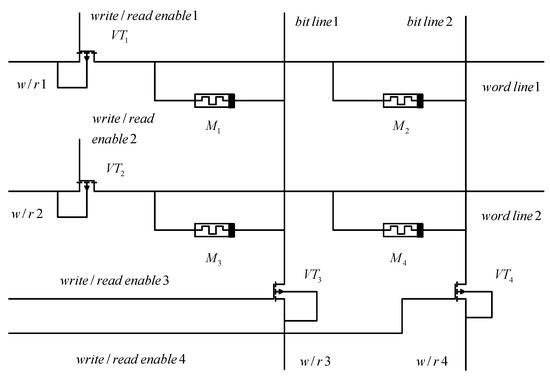
Figure 1.
A fragment of a hybrid memristor-based memory device.
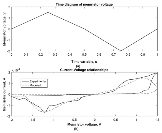
Figure 2.
(a) Time diagram of the applied memristor triangular voltage signal; (b) Comparison of the acquired I-V relationship to experimental data for the described triangular voltage signal.
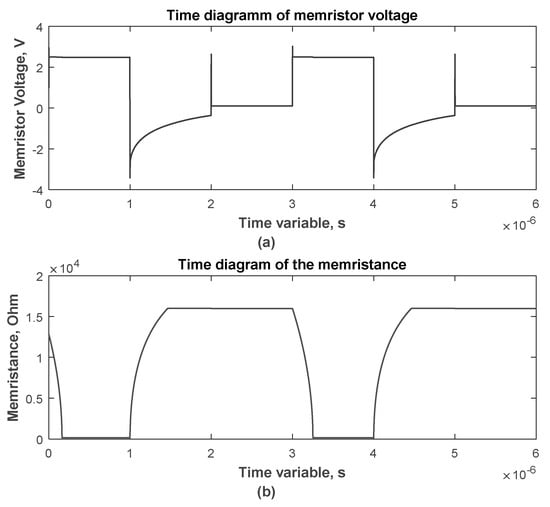
Figure 3.
(a) Time diagram of the memristor voltage across M1; (b) The corresponding change of the memristance of M1 during the simulation.
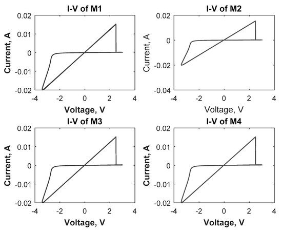
Figure 4.
Current-voltage relationships of the memristors derived during the analysis.
An advantage of the model [15,16] with the modified window function [17] used here compared to several existing models—e.g., GBCM, Biolek and Joglekar models—is the comparatively high nonlinearity extent of the dopant drift of the applied model and the possibility for realistic representation of the highly nonlinear relationship between the ionic drift and the voltage [10]. The respectable convergence of the computing procedures using the respective algorithm for simulations is also an advantage of the used model and the window function modified by the author [17]. The successful operation of a fragment of resistance-switching memory with the used memristor model and the modified window function for general pulse mode confirms that this memristor model, together with the modified window function, could be used for investigation of many memristor-based electronic circuits and devices.
A comparison between a single memristor memory cell, a 1T1R cell and a 4T4R memory scheme is madeaccording to several basic parameters and characteristics.The derived results are presented in Table 2 for illustration of the main properties of these devices.
Table 2.
Basic parameters and characteristics of a single memristor memory cell, 1T1R and 4T4R.
4. Conclusions
After analysis of the results derived by the simulations of the applied TiO2 memristor model with the applied modified window function and by the use of the original Biolek window function, it can be concluded that they have similar behavior during the memory operation processes, i.e., writing and reading information. The procedures of writing and reading in a fragment of a hybrid memory are successfully analyzed with the applied memristor model and the modified window function. A good similarity is found between the received and experimental results. The I-V curves of the memory cell obtained by the applied model and the standard Biolek window function are almost identical to each other according to their range and shape. It canbe concluded that the model used here with the modified window function has the capability to represent the behavior of a memristor in memory schemes for general pulse mode. After comparison of the I-V relationships with experimentally recorded I-V curves, it can be established that the model used here could realistically represent the behavior of the memristors in complex circuits and devices. An advantage of the applied model and the modified window function compared to the Pickett model is the established absence of convergence problems. Another advantage of the applied memristor model is the use of a highly nonlinear window function. The used memristor model is able to realistically represent the behavior of the memristor in electronic devices for high voltage signals without computational problems. The applied model could be used for representation of the memristor behavior for both soft-switching and hard-switching mode.
Funding
The research is supported by national Co-financing (contract NoДKOCT01/14) of COST Action No IC1401 MemoCIS by the National Science Fund of Bulgaria.
Acknowledgments
The author wants to thank to the National Science Fund of Bulgaria, who supported this research by national Co-financing (contract NoДKOCT01/14) of COST Action No IC1401 MemoCIS.
Conflicts of Interest
The author declares no conflict of interest.
References
- Dearnaley, G.; Stoneham, A.; Morgan, D. Electrical phenomena in amorphous oxide films. Rep. Prog. Phys. 1970, 33, 1129–1191. [Google Scholar] [CrossRef]
- Jeong, D.S.; Schroeder, H.; Waser, R. Coexistence of bipolar and unipolar resistive switching behaviors in a Pt/TiO2/Pt stack. Electrochem. Solid State Lett. 2007, 10, G51–G53. [Google Scholar] [CrossRef]
- Chua, L. Memristor—The Missing Circuit Element. IEEE Trans. Circuit Theory 1970, 18, 507–519. [Google Scholar] [CrossRef]
- Strukov, D.; Snider, G.; Stewart, D.; Williams, R.S. The Missing Memristor Found. Nat. Lett. 2008, 453, 80–83. [Google Scholar] [CrossRef] [PubMed]
- Joglekar, Y.; Wolf, S. The Elusive Memristor: Properties of Basic Electrical Circuits. Eur. J. Phys. 2009, 30, 661–675. [Google Scholar] [CrossRef]
- Biolek, Z.; Biolek, D.; Biolkova, V. SPICE Model of Memristor with Nonlinear Dopant Drift. Radioengineering 2009, 18, 210–214. [Google Scholar]
- Abdalla, H.; Pickett, M. SPICE modelling of memristors. IEEE Int. Symp. Circuits Syst. 2011, 1832–1835. [Google Scholar]
- Fleck, K.; la Torre, C.; Aslam, N.; Hoffmann-Eifert, S.; Böttger, V.; Menzel, S. Uniting Gradual and Abrupt SET Processes in Resistive Switching Oxides. Phys. Rev. Appl. 2016, 6, 064015. [Google Scholar] [CrossRef]
- Jiang, Z.; Wu, Y.; Yu, S.; Yang, L.; Song, K.; Karim, Z.; Wong, H.-P. A Compact Model for Metal-Oxide Resistive Random Access Memory With Experiment Verification. IEEE Trans. Electron Devices 2016, 63, 1884–1892. [Google Scholar] [CrossRef]
- Yang, J.; Pickett, M.D.; Li, X.; Ohlberg, D.A.A.; Stewart, D.R.; Williams, R.S. Memristive switching mechanism for metal/oxide/metal nanodevices. Nat. Nanotechnol. 2008, 3, 429–433. [Google Scholar] [CrossRef] [PubMed]
- Ascoli, A.; Corinto, F.; Tetzlaff, R. Generalized Boundary Condition Memristor Model. Int. J. Circuit Theory Appl. 2016, 44, 60–84. [Google Scholar] [CrossRef]
- Linn, E.; Siemon, A.; Waser, R.; Menzel, S. Applicability of Well-Established Memristive Models for Simulations of Resistive Switching Devices. IEEE Trans. Circuits Syst. I Regul. Pap. 2014, 61, 2402–2410. [Google Scholar] [CrossRef]
- Haron, N.; Hamdioui, S. On Defect Oriented Testing for Hybrid CMOS/Memristor Memory. IEEE Asian Test Symp. 2011, 353–358. [Google Scholar]
- Serb, A.; Redman-White, W.; Papavassiliou, C.; Prodromakis, T. Practical determination of individual element resistive states in selectorless RRAM arrays. IEEE Trans. Circuits Syst. I Regul. Pap. 2016, 63, 827–835. [Google Scholar] [CrossRef]
- Strukov, D.B.; Williams, R.S. Exponential ionic drift: Fast switching and low volatility of thin-film memristors. Appl. Phys. A Mater. Sci. Process. 2009, 94, 515–519. [Google Scholar] [CrossRef]
- Lehtonen, E.; Laiho, M. CNN using memristors for neighborhood connections. In Proceedings of the 2010 12th International Workshop on Cellular Nanoscale Networks and their Applications (CNNA 2010), Berkeley, CA, USA, 3–5 February 2010; pp. 1–4. [Google Scholar]
- Mladenov, V.; Kirilov, S. A Memristor Model with a Modified Window Function and Activation Thresholds. In Proceedings of the IEEE ISCAS 2018, Florence, Italy, 27–30 May 2018; pp. 1–5. [Google Scholar]
- Rashid, M. Introduction to PSpice Using OrCAD for Circuits and Electronics, 3rd ed.; Prentice Hall: Upper Saddle River, NJ, USA, 2004; ISBN 0-13-101988-0. [Google Scholar]
- Palm, W. Introduction to MATLAB for Engineers; McGraw-Hill: New York, NY, USA, 2011; ISBN 978-1-259-01205-1. [Google Scholar]
- Dozortsev, A.; Goldshtein, I.; Kvatinsky, S. Analysis of the row grounding technique in a memristor-based crossbar array. Int. J. Circuit Theory Appl. 2017, 1–16. [Google Scholar] [CrossRef]


© 2018 by the author. Licensee MDPI, Basel, Switzerland. This article is an open access article distributed under the terms and conditions of the Creative Commons Attribution (CC BY) license (http://creativecommons.org/licenses/by/4.0/).