Article

Zero Standby Solutions with Optical Energy Harvesting from a Laser Pointer

1
Lawrence Berkeley Labs, 1 Cyclotron Rd, Berkeley, CA 94720, USA
2
Department of Electrical Engineering and Computer Science, University of California Berkeley, Berkeley, CA 94720, USA
*
Author to whom correspondence should be addressed.
Electronics 2018, 7(11), 292; https://doi.org/10.3390/electronics7110292
Submission received: 25 September 2018 / Revised: 18 October 2018 / Accepted: 30 October 2018 / Published: 1 November 2018
(This article belongs to the Section Power Electronics)

Abstract

:
Despite recent efforts to reduce standby power consumption in plug loads, new trends in the miniaturization and wide distribution of electronics necessitates devices with zero standby consumption. This work introduces two zero standby solutions that wake a device using an external input of energy harvested from a 5 mW laser pointer. These solutions are applicable to electronics that are remotely activated or have a fiber optic connection. The first utilizes a cascoded header switch to allow for simultaneous low-voltage harvesting and high-voltage blocking. The second involves the use of a charge pump to boost the harvested voltage to a level appropriate for the gate of a high-voltage switch. Prototypes for each method are developed in order to demonstrate functionality and identify the associated benefits and drawbacks. The results show that combining the two methods allows for optimal activation range (up to 25 m) and component count.

1. Introduction and Background

1.1. Zero Standby Solutions

Standby power consumption by appliances, electrical devices, and other products continues to represent a significant use of energy. In the past decade, considerable progress has been achieved through a variety of policies and technologies. Most new low-voltage power supplies have no-load power consumption below 0.5 W, reflecting minimum energy efficiency standards in Europe, California, and elsewhere [1]. However, the last twenty years has seen an explosion in the number of devices that rely on power supplies and continuous power consumption [2]. The growth can be attributed to the proliferation of devices that require DC power, traditional AC-powered devices that now have electronics, and mobile devices with batteries. While the per-unit power consumption has fallen, the number of units continuously drawing power is rising. Modern electronic products have a diverse set of applications and requirements, which necessitates a wide variety of low-cost standby-reduction techniques.
Several solutions allow for zero standby consumption, which involves completely disconnecting the load from the supply power [3,4]. These solutions often use a sleep transistor, which can be implemented as either a footer or a header switch. As shown in Figure 1a, the footer switch is an N-type MOSFET (NMOS) that connects the ground of the main device to the ground of the power supply. Footer switches, due in part to their simplicity, cost, and reliability, have become a recent favorite in standby-reduction techniques [5]. The header switch, shown in Figure 1b, is a P-type MOSFET (PMOS) alternative that can be preferable in some applications [6].
The footer switch allows the main device to completely shut down, resulting in zero standby power consumption. However, the device can only turn on if a sufficient wake-up drive signal is provided to the footer switch gate. Footer switches can have drawbacks such as on-state resistance and leakage current, but these can often be mitigated by proper MOSFET selection. They also require the main device to latch the gate in an on state during operation.

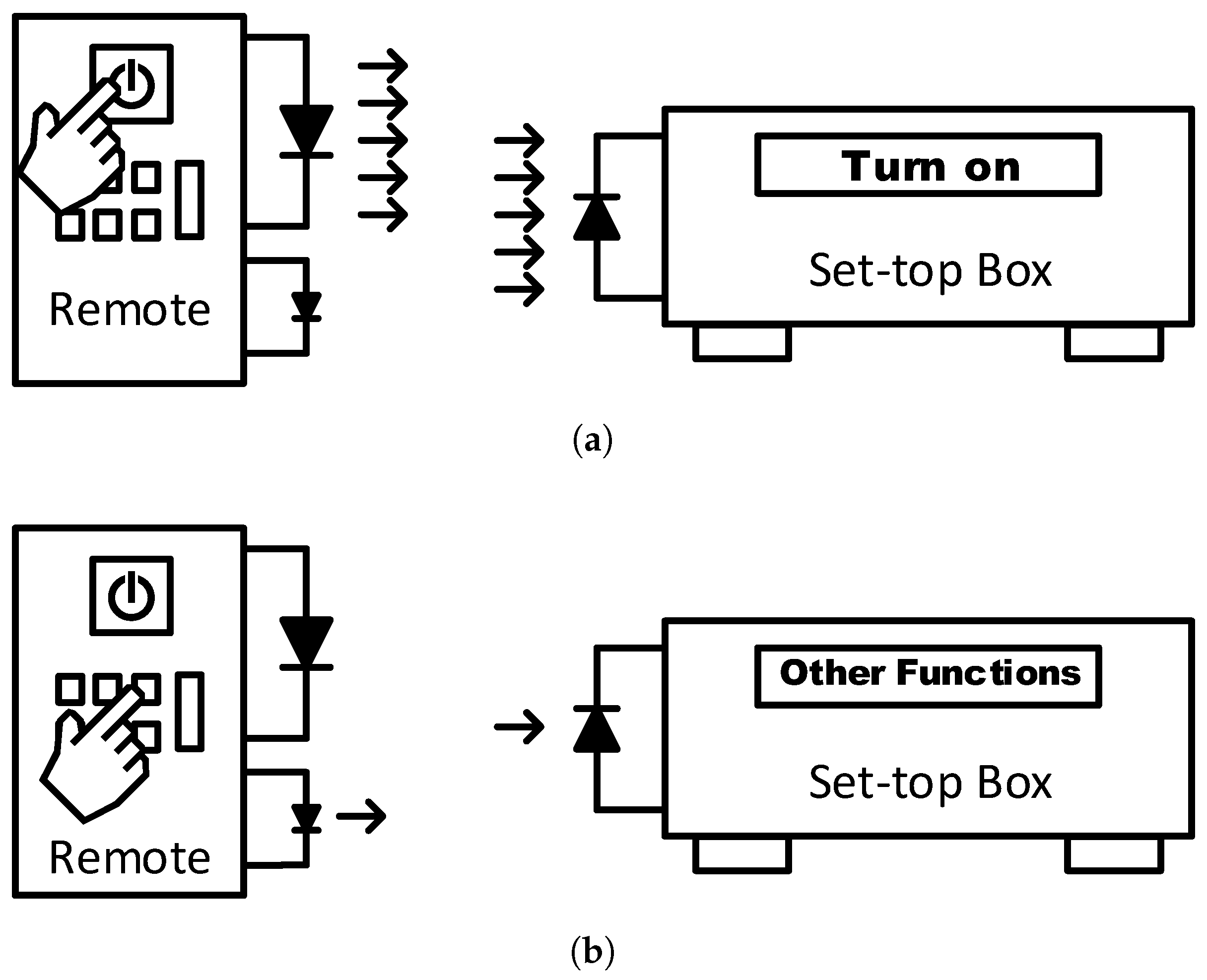
1.2. Optical Wake-Up Signal

Several works proposed zero standby solutions that harvest and utilize an optical wake-up signal [7,8,9,10,11,12,13,14,15,16,17]. These solutions have mainly been proposed for eliminating standby consumption in infrared (IR) receivers and processing units for set-top boxes. Nonetheless, they can also be applicable to many other remote non-wireless electronics such as lights, ceiling fans, and curtains. These applications all require a direct line of sight between user and device. Fading and dispersion losses are generally affected by the beam width and air quality, the latter of which may suffer in outdoors applications. Finally, high-power optical transmission may present safety concerns as a result of the potential for eye damage.
In 2015, Yamawaki and Serikawa [7,8] developed a method for driving the footer switch with harvested infrared energy. This method, shown in Figure 2, involves a two-stage IR transmission. To turn on the device, the remote control transmits a high-power IR signal, which is harvested by a photodiode array to activate the footer switch. Once the device is powered and latched, low-power IR signals are sufficient for all further communications. Normal operation of the appliance continues until the appliance receives a power-down signal, at which point the appliance unlatches the footer switch gate and becomes electrically isolated from the ground.
Although the solution in [7,8] can successfully maintain zero standby consumption, its transmission range is limited to 3 m. In addition, the prototype requires high-power pulsed optical transmission, which presents concerns in both power consumption and eye safety. Other past works yield similar range limitations. Kang et al. [9] developed a circuit to harvest power from a 15 mW IR laser to drive an electromechanical relay, but their prototype had a similar range of 2 m. Rosa et al. [10] also developed a relay-based architecture with a range of 2.5 m that could be extended to 7 m with a precisely positioned Fresnel lens. Utsunomiya et al. [11] demonstrated a harvesting circuit on a low-voltage integrated process that could be woken from 6 m by a 50 mW IR transmission. While their design is impressive in both range and power, it requires custom integrated hardware and is mainly intended for low-voltage battery-powered applications. Their circuit functions by detecting a rising edge in luminous intensity. Although simple and elegant, this method is susceptible to accidental triggering by ambient light or shadows. Finally, a drawback present in all IR-based solutions is that wide-beam transmissions may unintentionally wake other nearby devices.

1.3. Visible Laser Harvesting for Zero Standby

The laser-based solution is designed to overcome the practical shortcomings of the IR-based solutions discussed in Section 1.2. To summarize, these shortcomings are:
  • The range is fairly limited due to the wide LED angle.
  • Transmission at long range may require precise aiming, which is difficult with invisible IR transmission.
  • Wide-beam transmission may unintentionally wake adjacent devices that expect a similar IR wake-up signal.
  • Designs that require high-power transmission involve eye-safety concerns.
A laser-based solution is advantageous because of its narrow beam, which allows most of the light energy to be captured in a small photodetector die area. This characteristic allows for a nearly limitless transmission range, and removes the possibility of waking an adjacent device. In addition, a visible laser facilitates precise aiming. Finally, the common laser pointer can act as a universal remote and is easily purchased at a convenience store. In today’s market, many wirelessly-activated devices have their own communication protocols and dedicated remotes. The laser-based solution allows the possibility of using a low-cost laser pointer to activate a variety of loads from a variety of manufacturers. Despite these advantages, lasers have several challenges that must be addressed:
  • A laser pointer may be more difficult to aim for people with shaky hands. This shortcoming can be mitigated by increasing the area of the photodiode array as discussed in Appendix A, using a focusing lens at the receiver, or slightly increasing the laser’s beam width.
  • The laser beam is only wide enough to hit a single photodiode, which may not provide enough energy to harvest. This issue is addressed with the circuits discussed in Section 3.1 and Section 3.2.
  • Lasers incur even more stringent eye hazards than IR LEDs. As such, this work strictly limits its scope to class 3a visible laser pointers (<5 mW).
This work develops two front-end circuits that allow the harvested optical energy to provide a wake-up signal that drives the gate of a sleep transistor. These circuits are designed to achieve the following specifications:
  • The design achieves zero standby consumption and harvests an external energy input to generate a wake-up signal.
  • The design is constructed with commercial off-the-shelf (COTS) parts and does not require a custom integrated circuit.
  • The wake-up signal can be delivered with a common 5 mW class 3a laser pointer.
  • The design is applicable in power supplies at standard voltages such as 120 V AC or 48 V DC. This requires the design to be able to drive the gate of a high-voltage sleep transistor.
  • The wake-up signal can be generated within milliseconds of photodiode excitation.
The main design challenge is that power MOSFETs with a high drain-source breakdown voltage generally have a high gate-threshold voltage, and affordable COTS photodiodes cannot output the necessary voltage from a 5 mW laser input. To meet this challenge, Section 3 introduces two front-end circuit methods. These methods are guided by the photovoltaic models and characterization in Section 2. The first uses a cascoded topology that stacks two N-type MOSFETs: one with a low threshold voltage, and one with a high drain-source breakdown voltage. The second uses a Dickson charge pump to boost the photodiode voltage until it can activate the high-threshold power switch. Section 4 shows the experimental results and discusses the advantages of each design.

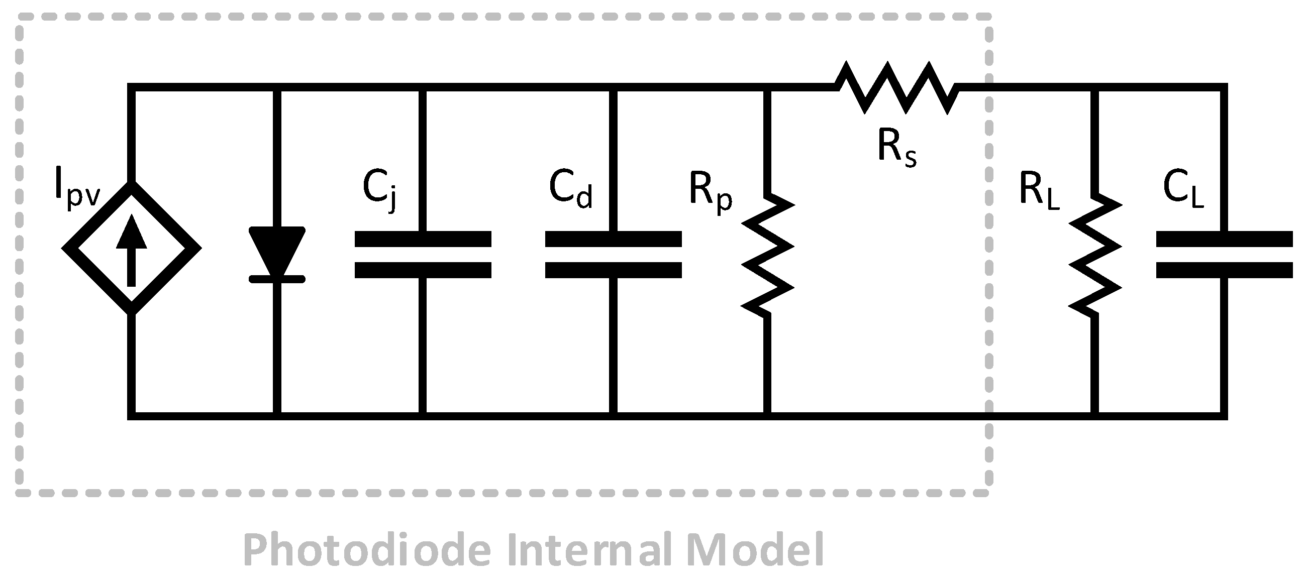
2. Photodiode Model and Characterization

Photodiodes may operate in photovoltaic or photoconductive mode, depending on whether the diode is forward or reverse biased, respectively [18]. Photoconductive mode has a relatively fast transient response, and is useful in high-speed optical communication and sensing. Optical harvesting applications operate the photodiode in photovoltaic mode, and generate power via the photovoltaic effect. Table 1 categorizes photodiode applications by their bias mode and operation frequency.
The photodiode equivalent circuit, shown in Figure 3, is modeled as a current source I p v in parallel with a diode [19,20]. Parasitics in this model include the series resistance R s , shunt resistance R p , junction capacitance C j , and diffusion capacitance C d . The prototypes in this work all use the Osram SFH206K photodiode, whose parasitics in Table 2 are estimated based on measurements and datasheet curves. The DC characteristics of a photodiode in photovoltaic mode, described in Section 2.1, are relevant for the cascoded header method discussed in Section 3.1. The AC characteristics, described in Section 2.2, are relevant for the charge pump discussed in Section 3.2. It is important to mention that these applications of optical harvesting focus on generating an output voltage large enough to activate the gate of an NMOS. As such, the photodiode measurements all focus on maximizing the output voltage, rather than the power.

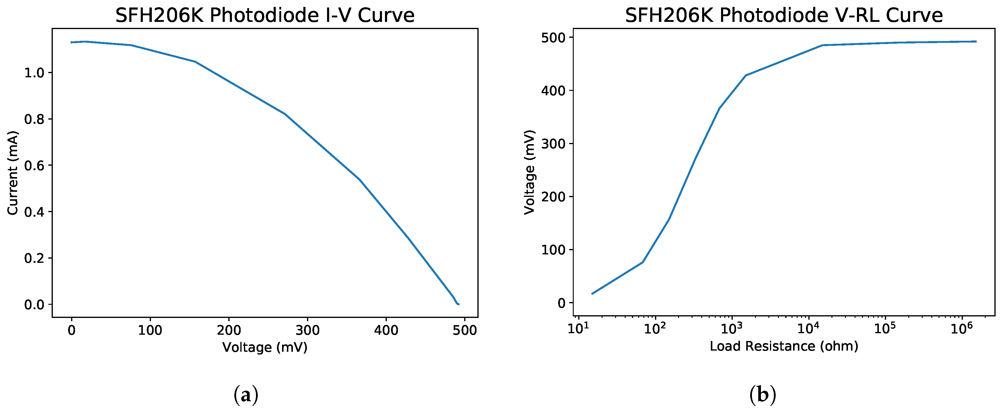
2.1. DC Characterization of a Photodiode

Like a solar cell, the DC operation of a photodiode depends solely on I p v , R s , and Rd. The parasitic capacitances C j and C d are only relevant in AC operation. Figure 4a shows the measured current-voltage relationship of an SFH206K subject to a 5 mW laser at a distance of 2 cm. I p v increases relative to the amount of incident light absorbed at the photodiode junction. Low-impedance loads will sink the current from I p v , resulting in a relatively low output voltage. However, high-impedance loads produce a relatively high-output voltage, which causes the diode in Figure 3 to become forward biased and sink most of I p v . This diode characteristic limits the open circuit voltage and causes the I-V curve in Figure 4a.
In optical zero-standby designs, the photodiode must ultimately produce a voltage suitable to drive the footer switch gate. As such, designs should place an emphasis on the photodiode output voltage. Since MOSFET gates are high impedance, the photodiode will output its open circuit maximum voltage when directly connected to the footer gate.

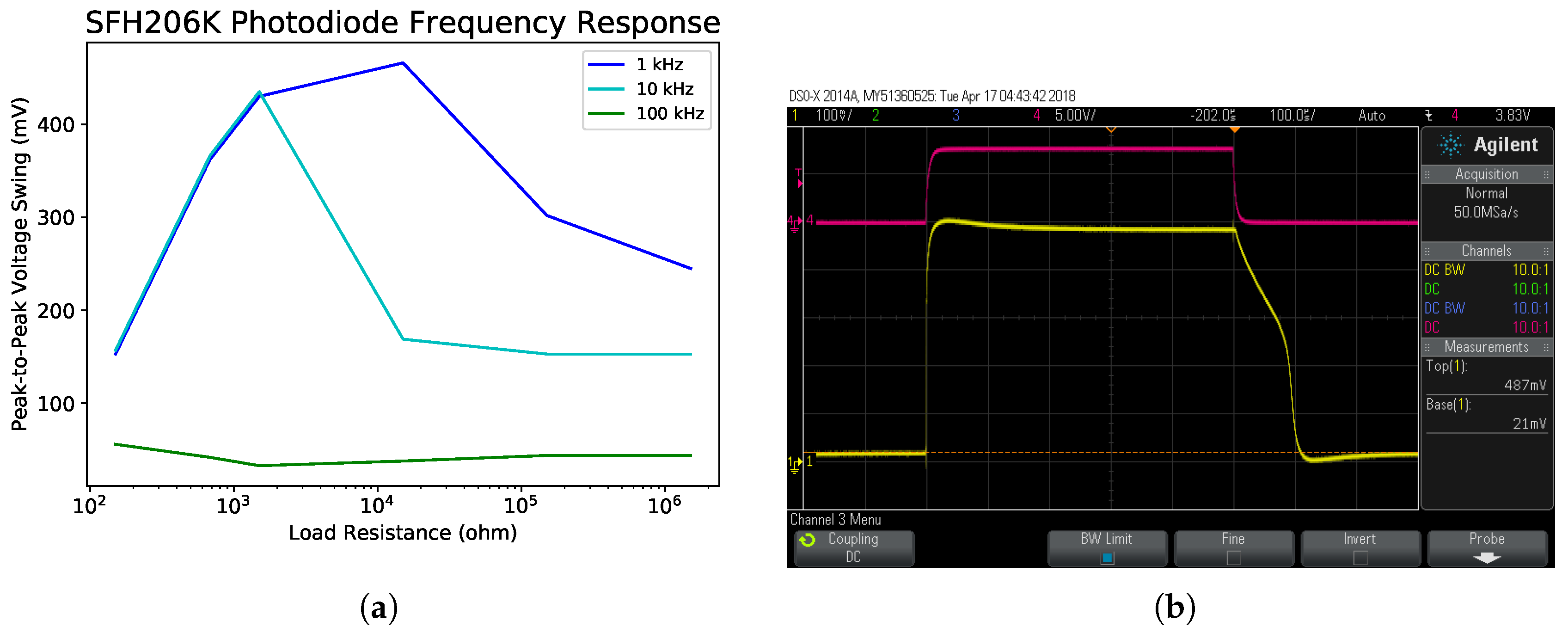
2.2. AC Characterization of a Photodiode

The AC characteristics of a photodiode are relevant for the charge pump design in Section 3.2, which requires an AC input and square-wave laser transmission. High-frequency photodiode applications include optical communications or sensing, all of which operate the photodiode in photoconductive mode. However, most applications of photovoltaic mode are in DC photovoltaic generation. This section explains the considerations of high-frequency photovoltaic operation that are relevant to developing the charge pump circuit.
The rise and fall times of a photodiode are determined from the total parallel capacitance at the output,
C t o t = C j + C d + C L .
The circuit model in Figure 3 shows that C t o t is comprised of the junction capacitance C j , the diffusion capacitance C d , and other capacitances C L at the output [21]. Note that R s is usually small enough that C L can be considered a parallel capacitance. The junction capacitance C j (also known as transition, depletion, or space charge capacitance) results from the parallel plate characteristics of the insulating depletion layer and the conducting P and N regions [22]. C j is dominant in reverse biased photoconductive mode or under a weak forward bias. Increasing the reverse bias decreases the junction capacitance, which is important for high-bandwidth optics. The diffusion capacitance C d (also known as the charge storage capacitance) results from the charge storage inherent in charge diffusion. C d is dominant in strong forward-biased photovoltaic modes.
The laser-based zero standby designs require the photodiode to operate in photovoltaic mode. Consequently, the diffusion capacitance C d dominates in the photodiode’s frequency response [22]. C d increases exponentially with the forward bias voltage V [23,24], and can be determined as [25,26]:
C d = τ e n k I o e e V n k T .
with minority carrier lifetime τ , electron charge e, temperature T, and diode factor n. A strong forward bias can result in very slow and nonlinear rise and fall transients. In Figure 5b, the yellow waveform is the voltage across a photodiode with pulsed laser input and a 15 kΩ load resistance. The bent falling edge is a result of discharging the nonlinear C d through R L .
For low-voltage harvesting, it is important to maximize the AC input to the charge pump. As such, R L is set so as to maximize the photodiode’s peak-to-peak output voltage swing. Figure 5a shows the output voltage of the SFH206K photodiode as a function of frequency and R L . Naturally, increasing the frequency decreases the output voltage swing due to the R L C d filter. The optimal R L is measured to be roughly 15 kΩ at 1 kHz. In general, sizing R L negotiates a trade-off between high-output DC voltage (high R L ), and quick fall time (low R L ).
When the laser switches on, I p v charges C d , resulting in the rise transient shown in Figure 5b. Likewise, the fall transient in Figure 5b occurs when the laser switches off, and C d drains through R L . An R L value of 15 kΩ causes the fall time to be relatively slow, and the effects of the nonlinear capacitance C d are more apparent. When the output voltage drops to a certain level, the dominant capacitance switches from C d to C j + C L , resulting in the fall transient’s irregular shape [26,27].

3. Laser-Based Wake-Up Circuit Solutions

This work introduces two laser-based zero standby circuits with the specifications discussed in Section 1.3. The first solution presents a cascoded version of the header switch from Figure 1b. The second solution involves using a Dickson charge pump to drive the gate of a high-voltage footer switch. Note that either method can be applied in a footer- or header-based zero standby topology.

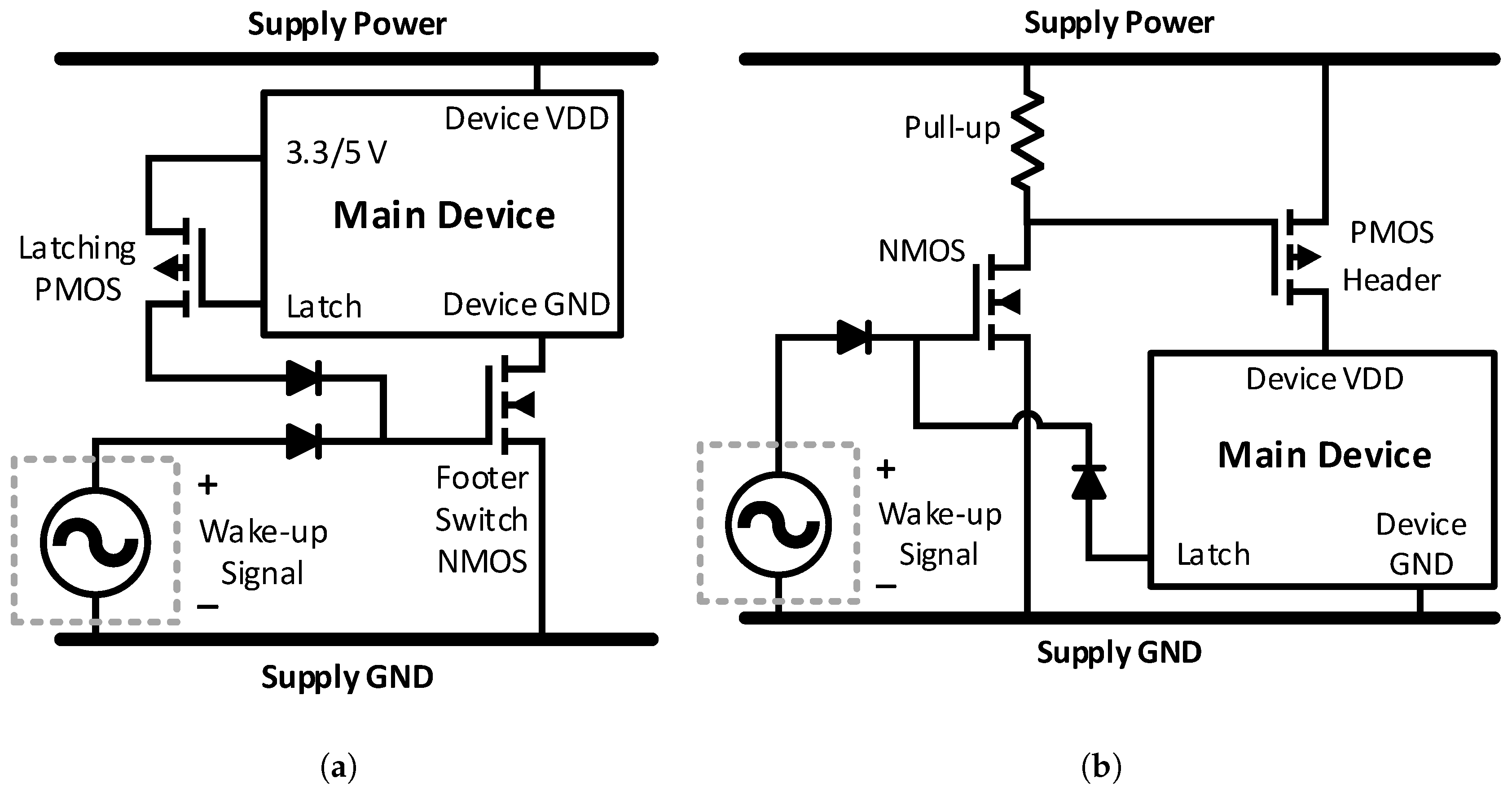
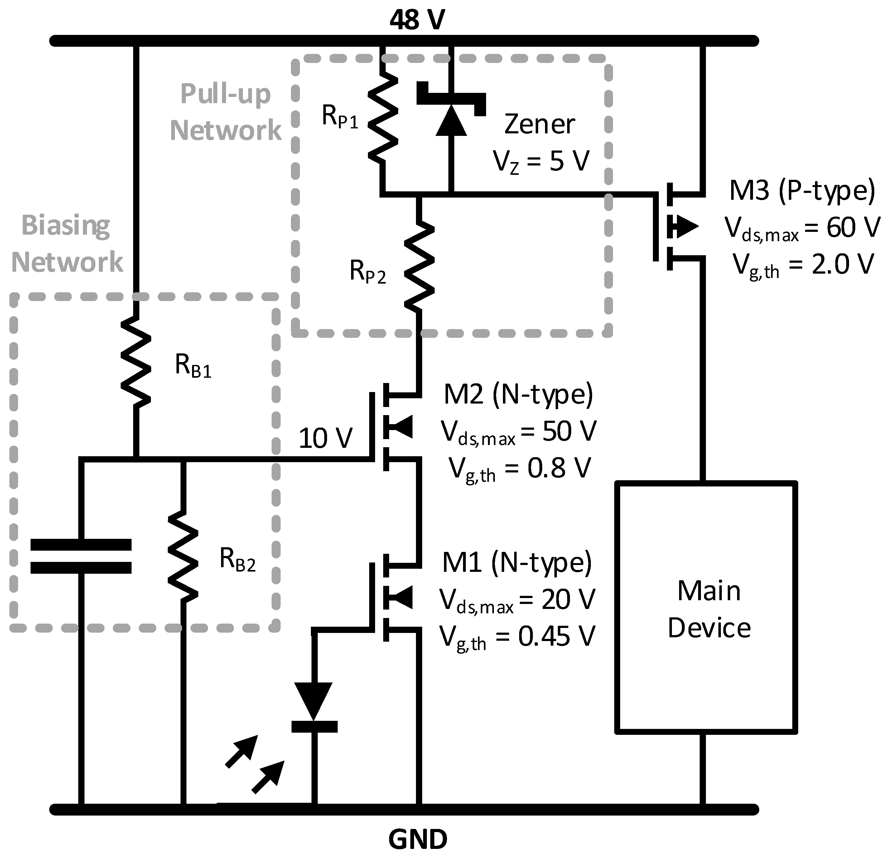
3.1. Solution with a Cascoded Header Switch

In order to withstand high voltage, a MOSFET switch requires a high maximum drain-source voltage, Vds,max. However, in order to functionally activate on a harvested low-voltage input, the MOSFET requires a low gate-threshold voltage, Vg,th. As shown in Table 3, there is a trade-off between a low Vg,th and high Vds,max. Most COTS MOSFETs cannot simultaneously satisfy both requirements. The cascoded header, shown in Figure 6, upgrades the header switch (Figure 1b) to allow for a higher supply voltage. Figure 6 illustrates an example that uses the devices in Table 3 in a 48 V power over Ethernet (PoE) application. In this circuit, M1 is selected with a low Vg,th, while M2 and M3 both have high Vds,max. Such a combination of MOSFETs allows for both a low turn-on voltage and a high supply voltage.

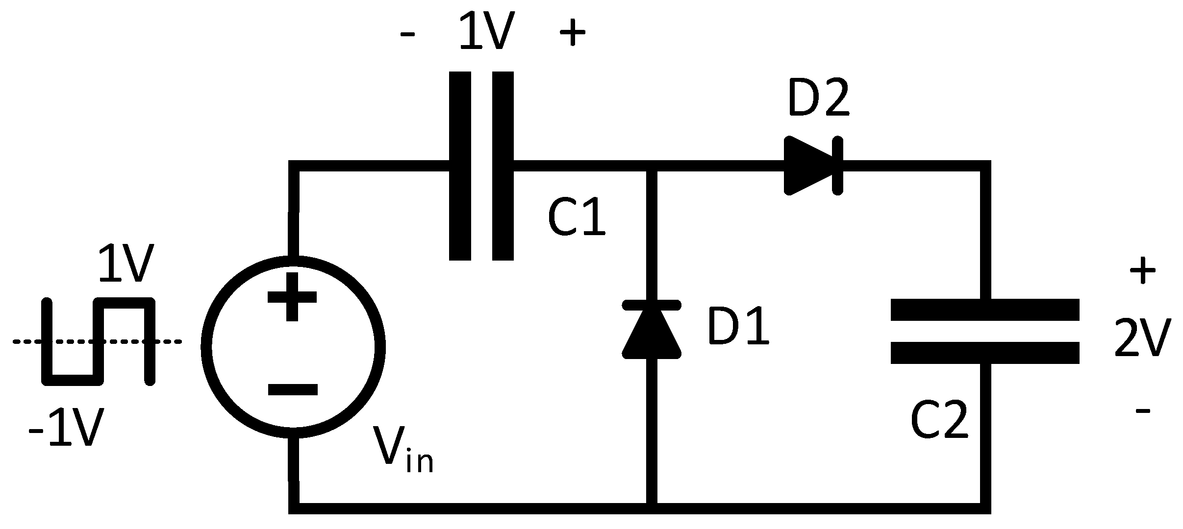
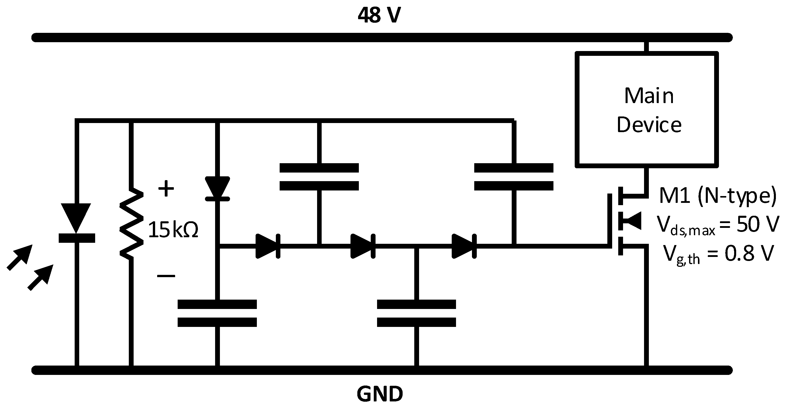
3.2. Solution with a Dickson Charge Pump

As mentioned in Section 3.1, MOSFETS with a high Vds,max often have a high Vg,th. This section proposes a method to activate the footer switch by stepping-up the photodiode output voltage using a Dickson charge pump. The Dickson charge pump is a switch-capacitor circuit that can rectify and multiply the AC input voltage by an integer multiple [13,28,29,30,31,32,33,34,35,36,37,38]. This work uses the Dickson charge pump in its passively self-powered configuration. Other similar charge pump step-up circuits require an external clock signal, which is not available in zero standby applications. The Villard charge pump is another passive option, and it has been shown that the Dickson and Villard charge pumps have a similar performance [33].
Figure 7 shows a two-stage passive Dickson charge pump, also known as a Greinacher doubler. Although Figure 7 shows the input Vin as a square wave with 1 V amplitude, the doubler works for any AC waveform if the flying capacitors are sufficiently sized. In the first phase, Vin swings negative and charges capacitor C1 to 1 V. During the second phase, the voltage across C1 stacks with the input voltage, which charges C2 to 2 V. In this way, the input voltage is rectified and doubled.
Previous works propose the Dickson charge pump as a step-up rectifier in energy harvesting applications. Of these, the optical harvesting applications all involve stepping up the output voltage of photovoltaics with an actively-clocked charge pump [13,28,29]. The passive Dickson charge pump is popular in RF energy harvesting circuits as a step-up rectifier, since the antenna’s output voltage is rarely high enough to power integrated electronics [33,34,35,36,37]. In RF applications, the antenna must be coupled to the charge pump via a matching network. The Dickson charge pump is attractive because its straightforward input resistance analysis aids in designing a matching network.
This work focuses on optical harvesting as a means of generating a wake-up signal. As such, the passive charge pump must generate a high-output voltage to activate the gate of a high-voltage NMOS. Relatively little power is required to charge the gate capacitance, and so the charge pump’s design focuses on output voltage, rather than output power. In this way, the designs in this work do not require a matching network, unlike those in RF harvesting applications.
Another difference between optical and RF harvesting is the frequency of operation. In optical harvesting, the large photodiode diffusion capacitance makes high-frequency operation very difficult. Figure 5 shows that for a SFH206K photodiode, the greatest voltage swing can be achieved at low frequency due to the relatively long discharge transient. The design in this work transmits optical power at 1 kHz and uses a 15 kΩ load resistor in parallel with the photodiode to generate a high-voltage swing.
Overall, the charge pump design in this work is very simple and has flexibility in component selection. The circuit design, shown in Figure 8, is similar to the two-stage Dickson design in Figure 7. Since the NMOS gate load is essentially an open circuit, power transfer is irrelevant to the design. Various analyses of the Dickson charge pump input impedance [36,37,38] are unnecessary when R L and C d dominate the photodiode fall time. Finally, various guidelines for sizing the flying capacitors [36,37] are also unnecessary at 1 kHz operation. At 1 kHz, the flying capacitors will be fully charged every cycle, and should be at least ten times larger than the gate capacitance.

4. Results and Discussion

Prototypes were constructed to test the methods presented in Section 3.1 and Section 3.2. These experiments also provided insight into the advantages and disadvantages of each method.

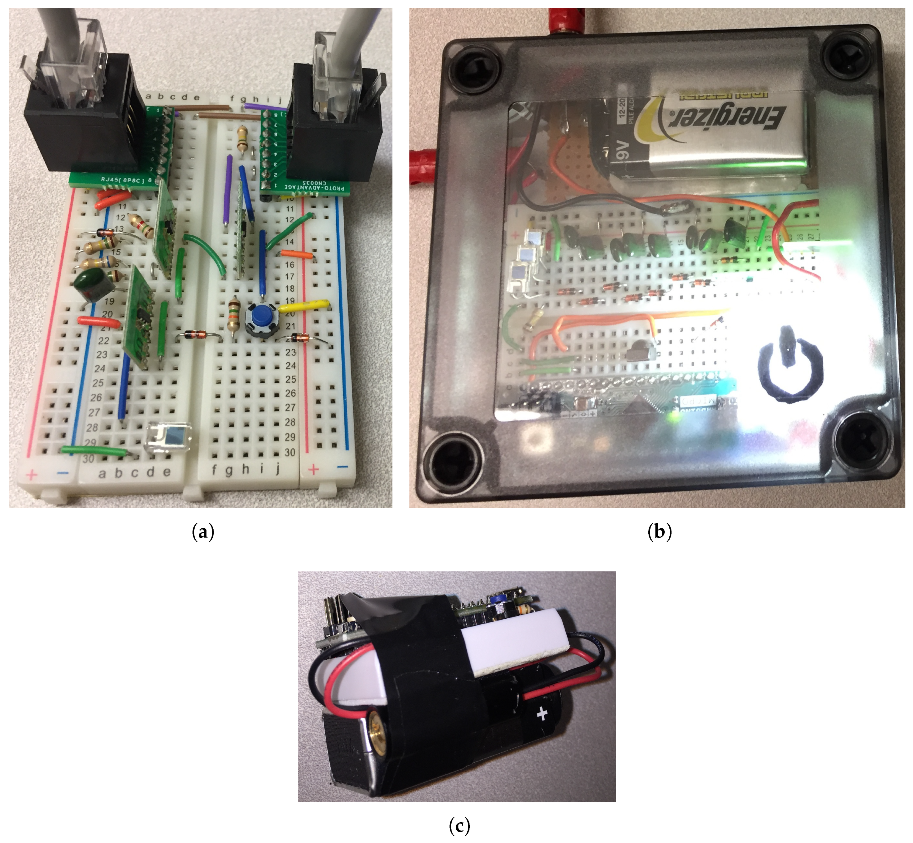
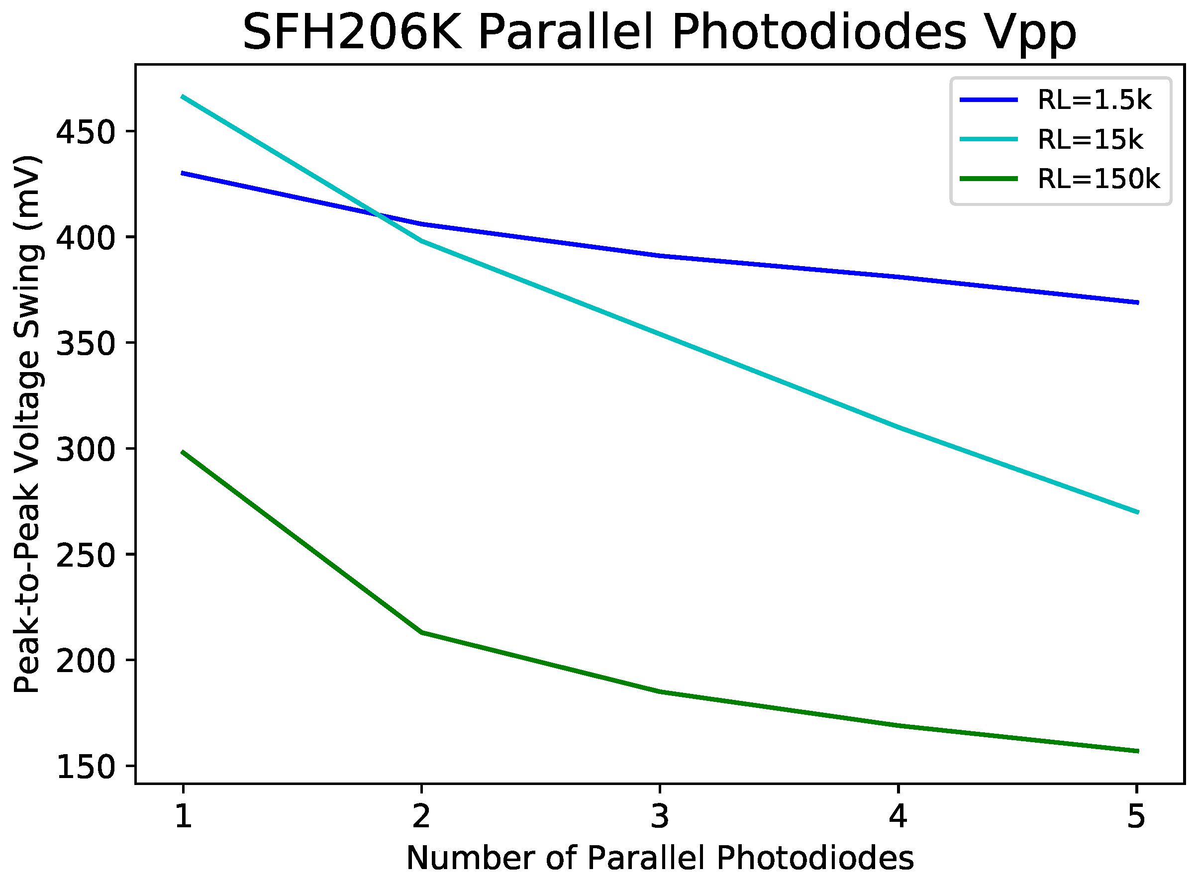
4.1. Prototypes and Results

The prototypes, shown in Figure 9, were constructed from COTS parts, including the MOSFETs in Table 3. The transmitter in Figure 9c uses a conventional 5 mW laser pointer, which can optionally be pulsed at 1 kHz. The two receivers showcase different applications of the laser-based solution. In Figure 9a, the cascoded method is used to connect PoE to a 48 V DC fan. The prototype in Figure 9b uses a charge pump and photodiode array to eliminate standby consumption in a battery-powered lamp.
Both prototypes demonstrate the intended functionality. Table 4 shows the maximum activation distance of the prototypes in various configurations. The cascoded method has the lowest range at 7 m, which is still greater than most previous works [7,8,9,10,11]. Increasing the number of charge pump stages and photodiodes yields a range of 25 m. At such distances, the laser’s beam width becomes noticeable, which helps with aiming but dilutes the incident light energy on each photodiode. Greater activation range is possible with a proper balance between these two factors. On a human interaction time scale, both prototypes activate instantaneously. On a finer time scale, the charge pump is several milliseconds slower, depending on the number of stages. Both prototypes achieve practically zero standby consumption, although the cascode’s standby consumption is technically nonzero (<1 μ W) due to the biasing circuit.

4.2. Discussion of Laser-Based Standby Methods

An important result of this work is to compare the two laser-based zero standby methods, and the prototypes assist in studying the practical advantages and disadvantages of each. The cascode’s main advantage is that it requires a fixed number of components, all of which can be easily integrated on chip if desired. In contrast, the charge pump may require many components to activate an NMOS with a relatively high Vg,th. In addition, the cascode can be activated by a common household laser pointer, whereas the charge pump requires a special pulsed transmission. The main disadvantage of the cascode is that there is little margin of error between the photodiode’s maximum open circuit voltage of 492 mV (Figure 4) and the NMOS Vg,th of 450 mV (M1 in Figure 6). Consequently, diffused or angled illumination may fail to activate the device. In addition, the beam’s divergence limits the range to 7 m as shown in Table 4. Another disadvantage of this topology is that a poor gate-biasing circuit may draw significant standby power.
The charge pump also has its own list of attractive qualities. First, the charge pump requires several cycles of pulsed input, which makes it fairly resistant to accidental activation by ambient light. If desired, a filter can ensure activation only occurs with a 1 kHz input. Another benefit of the charge pump is that its output can be much higher than Vg,th, making the circuit fairly reliable. The main disadvantage of the charge pump is from the 0.2 V Schottky diode drop. With R L = 15 kΩ, the photodiode can output up to 487 mV at 1 kHz (Figure 5a). However, as a result of the diode drop, only 287 mV gets transferred to each stage in the charge pump, making the circuit unexpectedly inefficient in low-voltage applications. In addition, Schottky diodes are unavailable on many integrated processes.
A combination of the two methods may well be the best solution. This combination would utilize a charge pump as the front end to a cascoded header switch. The charge pump would increase the circuit’s reliability and make it resistant to accidental activation by ambient light. The cascoded header would reduce the requisite number of charge pump stages. As shown in Table 4, designers can vary the number of stages based on specifications for range, reliability, size, and cost.

5. Conclusions

This work introduces a laser-based optical wake-up solution for zero-standby plug loads. In order to utilize commercial off-the-shelf parts to wake devices at typical plug voltages, this work develops two circuit methods. The first uses a cascoded header switch, and the second uses a Dickson charge pump to activate a footer switch. Each method has its advantages, and it is possible that a combination of methods is the optimal solution. Zero standby solutions will be very important in reducing consumption in future plug-load electronics. The wide diversity of electronics necessitates a portfolio of solutions, each of which have a specific application. The laser-based solutions introduced in this work are easy to implement, and can greatly reduce the consumption in devices that expect a remote line-of-sight wake-up signal. Future work may add a simultaneous information and power capability and extend the application space to fiber optics.

Author Contributions

The authors had the following contributions: conceptualization, A.M. and D.G.; methodology, D.G. and R.H.; software, D.G.; validation, D.G.; formal analysis, D.G.; investigation, D.G.; resources, A.M.; data curation, D.G.; writing—original draft preparation, D.G.; writing—review and editing, A.M., R.H., and R.L.; visualization, A.M. and D.G.; supervision, A.M.; project administration, A.M.; funding acquisition, A.M.

Funding

This research was funded by the California Energy Commissions EPIC Project grant number EPC-15-024.

Acknowledgments

Special thanks to the reviewers, editors, and industry collaborators in Power Integrations, Delta Electronics, and Belkin.

Conflicts of Interest

The authors declare no conflict of interest.

Appendix A. Array of Photodiodes

Laser-based zero standby devices can benefit from incorporating an array of photodiodes. The array effectively increases the light-sensitive area, making it easier to aim the laser pointer at long distances. Photovoltaic arrays for solar generation are commonly configured as parallel strings of series panels. Series or parallel connections each have their advantages and disadvantages under various types of shading conditions [39,40,41]. For laser harvesting, only a single cell of the array will be illuminated, and the other cells can be considered as fully shaded. However, the laser-based zero standby solutions are mostly indifferent to the array’s output power, and only require a high-output voltage. As such, the design considerations are somewhat different than for photovoltaic generation.
Photodiodes can be stacked in series, with the output voltage as the total voltage across the stack. The illumination of a single photodiode would still cause that photodiode to output its open-circuit voltage, and increase the total stack voltage by that amount. While the cascoded solution (Section 3.1) could use a series array, it is not recommended because the stack voltage in ambient light can easily exceed the gate threshold Vg,th of the footer switch. A series array works well in the charge pump solution (Section 3.2), although this solution strictly requires that a load resistor R L be placed across each photodiode in the stack. Nonetheless, if this requirement is met, the peak-to-peak voltage swing of the entire stack is identical to that of the illuminated photodiode.
Photodiodes can also be aligned in parallel. The array’s output voltage is heavily influenced by the additional parasitics of the non-illuminated photodiodes. First, the open-circuit voltage of the entire array is limited by the photodiode with the lowest diode drop. Second, the diffusion capacitance C d is effectively multiplied by the array size, adding some complication to the design of the charge pump solution. As shown in Figure A1, the peak-to-peak voltage of a single photodiode is greatest with a 15 kΩ load resistance. However, an array of photodiodes requires a lower load resistance in order to drain the combined diffusion capacitance.
Overall, the best solution may well be a series string of parallel cells. Such an array would lower the number of parallel photodiodes per cell, while also reducing the number of required load resistors. Photodiode arrays of this sort could be etched as a single component, but would differ from standard photovoltaic panels in that they would have a smaller cell area and more series connections.
Figure A1. Peak-to-peak voltage swing of an array of parallel SFH206K photodiodes, in which only one of them is illuminated by a 5 mW laser at 2 cm switching at 1 kHz. Adding photodiodes generally increases the parallel capacitance and the fall time. With two or more photodiodes, a lower load resistance (1.5 kΩ) is necessary to quickly drain the combined parasitic capacitances.
Electronics 07 00292 g0a1

References

  1. Ore, D. More Data, Less Energy Making Network Standby More Efficient in Billions of Connected Devices; International Energy Agency: Paris, France, 2014. [Google Scholar]
  2. Comstock, O.; Jarzomski, K. Consumption and saturation trends of residential miscellaneous end-use loads. In Proceedings of the 2012 ACEEE Summer Study Energy Efficiency Buildings, Pacific Grove, CA, USA, 14 August 2012. [Google Scholar]
  3. Ellis, M.; Siderius, H.P.; Lane, K. Closing the Gap towards Net Zero Energy Appliances. In Proceedings of the ECEEE 2015 Summer Study, Toulon, France, 1–6 June 2015. [Google Scholar]
  4. Meier, A.; Siderius, H.P. Should The Next Standby Power Target Be 0-Watt? 2017. Available online: https://escholarship.org/uc/item/566951pn (accessed on 24 September 2018).
  5. Fukuoka, K.; Maeda, N.; Nii, K.; Fujigaya, M.; Sakamoto, N.; Koike, T.; Irita, T.; Wakahara, K.; Matsuyama, T.; Hasegawa, K.; et al. Power-Management Features of R-Mobile U2, an Integrated Application Processor and Baseband Processor. IEEE Micro 2013, 33, 26–36. [Google Scholar] [CrossRef]
  6. Chao, B.; Harrison, L. Re-Designing Normally-on Load Switches with Zero-Power MOSFETs Reduces Power Consumption. Advanced Linear Devices White Paper. 2008. Available online: https://www.aldinc.com/pdf/ZeroPowerNormallyONSwitch.pdf (accessed on 24 September 2018).
  7. Yamawaki, A.; Serikawa, S. An extending method of operable distance for infrared remote controlled power switch with zero stand-by power. In Proceedings of the 2015 International Conference on Informatics, Electronics & Vision (ICIEV), Fukuoka, Japan, 15–18 June 2015; pp. 1–5. [Google Scholar]
  8. Yamawaki, A.; Serikawa, S. Power supply circuit with zero standby power consumption on infrared remote controlled product by using energy harvesting. In Proceedings of the 2015 International MultiConference of Engineers and Computer Scientists, Hong Kong, China, 18–20 March 2015. [Google Scholar]
  9. Kang, S.; Park, K.; Shin, S.; Chang, K.; Kim, H. Zero standby power remote control system using light power transmission. IEEE Trans. Consum. Electron. 2011, 57, 1622–1627. [Google Scholar] [CrossRef]
  10. Rosa, R.L.; Aiello, N.; Zoppi, G. An Innovative System Capable to Turn on Any Turned Off electrical appliance by means of an efficient optical energy transfer. In Proceedings of the International Exhibition and Conference for Power Electronics, Intelligent Motion, Renewable Energy and Energy Management (PCIM Europe 2014), Nuremberg, Germany, 20–22 May 2014; pp. 1–8. [Google Scholar]
  11. Utsunomiya, F.; Tanaka, A.; Douseki, T. A self-powered photosensor switch detects only rising edge of infrared-light pulse for wireless zero-standby-power wake-up receiver. In Proceedings of the 2013 IEEE SENSORS, Baltimore, MD, USA, 3–6 November 2013; pp. 1–4. [Google Scholar] [CrossRef]
  12. Haydaroglu, I.; Mutlu, S. Optical power delivery and data transmission in a wireless and batteryless microsystem using a single light emitting diode. J. Microelectromech. Syst. 2015, 24, 155–165. [Google Scholar] [CrossRef]
  13. Ferro, E.; Illade-Quinteiro, J.; Brea, V.; López, P.; Cabello, D.; Doménech-Asensi, G. The Dickson charge pump as voltage booster for light energy harvesting on CMOS vision chips. In Proceedings of the 2014 14th International Workshop on Cellular Nanoscale Networks and their Applications (CNNA), Notre Dame, IN, USA, 29–31 July 2014; pp. 1–2. [Google Scholar]
  14. Qian, Z.; Kang, S.; Rajaram, V.; Cassella, C.; McGruer, N.E.; Rinaldi, M. Zero-power light-actuated micromechanical relay. In Proceedings of the 2017 IEEE 30th International Conference on Micro Electro Mechanical Systems (MEMS), Las Vegas, NV, USA, 22–26 January 2017; pp. 940–941. [Google Scholar]
  15. Mathews, J.; Barnes, M.; Young, A.; Arvind, D. Low power wake-up in wireless sensor networks using free space optical communications. In Proceedings of the 2010 Fourth International Conference on Sensor Technologies and Applications (SENSORCOMM), Venice, Italy, 18–25 July 2010; pp. 256–261. [Google Scholar]
  16. Kim, G.; Lee, Y.; Bang, S.; Lee, I.; Kim, Y.; Sylvester, D.; Blaauw, D. A 695 pW standby power optical wake-up receiver for wireless sensor nodes. In Proceedings of the Custom Integrated Circuits Conference (CICC), San Jose, CA, USA, 9–12 September 2012; pp. 1–4. [Google Scholar]
  17. Lim, W.; Jang, T.; Lee, I.; Kim, H.S.; Sylvester, D.; Blaauw, D. A 380pW dual mode optical wake-up receiver with ambient noise cancellation. In Proceedings of the 2016 IEEE Symposium on VLSI Circuits (VLSI-Circuits), Honolulu, HI, USA, 15–17 June 2016; pp. 1–2. [Google Scholar]
  18. OSI OptoElectronics. Photodiode Characteristics and Applications. Available online: http://www.osioptoelectronics.com/application-notes/AN-Photodiode-Parameters-and-Characteristics.pdf (accessed on 24 September 2018).
  19. Cubas, J.; Pindado, S.; de Manuel, C. Explicit expressions for solar panel equivalent circuit parameters based on analytical formulation and the Lambert W-function. Energies 2014, 7, 4098–4115. [Google Scholar] [CrossRef]
  20. Park, H.; Kim, H. PV cell modeling on single-diode equivalent circuit. In Proceedings of the IECON 2013-39th Annual Conference of the IEEE Industrial Electronics Society, Vienna, Austria, 10–13 November 2013; pp. 1845–1849. [Google Scholar]
  21. Schwarzburg, K.; Willig, F. Diffusion impedance and space charge capacitance in the nanoporous dye-sensitized electrochemical solar cell. J. Phys. Chem. B 2003, 107, 3552–3555. [Google Scholar] [CrossRef]
  22. Hu, C. Modern Semiconductor Devices for Integrated Circuits; Prentice Hall: Upper Saddle River, NJ, USA, 2010; Volume 1. [Google Scholar]
  23. Schlosser, V.; Ghitas, A. Measurement of silicon solar cells AC parameters. In Proceedings of the Arab Regional Solar Energy Conference, Zallaq, Bahrain, 5–7 November 2006. [Google Scholar]
  24. Yamamoto, Y. Fundamentals of Noise Processes; Cambridge University Press: Cambridge, UK, 2017. [Google Scholar]
  25. Özden, S.; Bayhan, H.; Dönmez, A.; Bayhan, M. Measurement and comparison of silicon PIN-photodiodes with AC impedance at different voltages. Semiconductors 2008, 42, 834–837. [Google Scholar] [CrossRef]
  26. Kumar, R.; Suresh, M.; Nagaraju, J. Silicon (BSFR) solar cell AC parameters at different temperatures. Sol. Energy Mater. Solar Cells 2005, 85, 397–406. [Google Scholar] [CrossRef]
  27. Kumar, R.A.; Suresh, M.; Nagaraju, J. Time domain technique to measure solar cell capacitance. Rev. Sci. Instrum. 2003, 74, 3516–3519. [Google Scholar] [CrossRef]
  28. Brea, V.M.; Suarez, M.; Illade-Quinteiro, J.; López, P.; Cabello, D.; Doménech-Asensi, G. Voltage boosters for on-chip solar cells on focal-plane processors. In Proceedings of the 2013 IEEE 20th International Conference on Electronics, Circuits, and Systems (ICECS), Abu Dhabi, UAE, 8–11 December 2013; pp. 393–396. [Google Scholar]
  29. Çilingiroğlu, U.; Tar, B.; Özmen, Ç. On-chip photovoltaic energy conversion in bulk-CMOS for indoor applications. IEEE Trans. Circuits Syst. I Regul. Pap. 2014, 61, 2491–2504. [Google Scholar] [CrossRef]
  30. Dickson, J.F. On-chip high-voltage generation in MNOS integrated circuits using an improved voltage multiplier technique. IEEE J. Solid-State Circuits 1976, 11, 374–378. [Google Scholar] [CrossRef]
  31. Ki, W.H.; Lu, Y.; Su, F.; Tsui, C.Y. Analysis and design strategy of on-chip charge pumps for micro-power energy harvesting applications. In Proceedings of the IFIP/IEEE International Conference on Very Large Scale Integration-System on a Chip, Hong Kong, China, 3–5 October 2011; Springer: Berlin/Heidelberg, Germany, 2011; pp. 158–186. [Google Scholar]
  32. Tanzawa, T. On-Chip High-Voltage Generator Design; Springer: Berlin/Heidelberg, Germany, 2013. [Google Scholar]
  33. Yan, H.; Montero, J.M.; Akhnoukh, A.; De Vreede, L.C.; Burghartz, J. An integration scheme for RF power harvesting. In Proceedings of the STW Annual Workshop on Semiconductor Advances for Future Electronics and Sensors, Veldhoven, The Netherlands, 17–18 November 2005; pp. 64–66. [Google Scholar]
  34. Marshall, B.R.; Morys, M.M.; Durgin, G.D. Parametric analysis and design guidelines of RF-to-DC Dickson charge pumps for RFID energy harvesting. In Proceedings of the 2015 IEEE International Conference on RFID (RFID), San Diego, CA, USA, 15–17 April 2015; pp. 32–39. [Google Scholar]
  35. Muramatsu, M.; Koizumi, H. An experimental result using RF energy harvesting circuit with Dickson charge pump. In Proceedings of the 2010 IEEE International Conference on Sustainable Energy Technologies (ICSET), Kandy, Sri Lanka, 6–9 December 2010; pp. 1–4. [Google Scholar]
  36. Schemmel, D. A Wireless Energy Harvesting System with Beamforming Capabilities. Ph.D. Thesis, Colorado School of Mines, Golden, CO, USA, 2017. [Google Scholar]
  37. De Vita, G.; Iannaccone, G. Design criteria for the RF section of UHF and microwave passive RFID transponders. IEEE Trans. Microw. Theory Tech. 2005, 53, 2978–2990. [Google Scholar] [CrossRef]
  38. Seeman, M.D.; Sanders, S.R. Analysis and optimization of switched-capacitor DC–DC converters. IEEE Trans. Power Electron. 2008, 23, 841–851. [Google Scholar] [CrossRef]
  39. Gao, L.; Dougal, R.A.; Liu, S.; Iotova, A.P. Parallel-Connected Solar PV System to Address Partial and Rapidly Fluctuating Shadow Conditions. IEEE Trans. Ind. Electron. 2009, 56, 1548–1556. [Google Scholar] [CrossRef] [Green Version]
  40. Chatterjee, A.; Keyhani, A.; Kapoor, D. Identification of photovoltaic source models. IEEE Trans. Energy Convers. 2011, 26, 883–889. [Google Scholar] [CrossRef]
  41. Mäki, A.; Valkealahti, S. Power losses in long string and parallel-connected short strings of series-connected silicon-based photovoltaic modules due to partial shading conditions. IEEE Trans. Energy Convers. 2012, 27, 173–183. [Google Scholar] [CrossRef]
Figure 1. (a) The footer switch requires a wake-up signal to connect the device ground to supply ground. The main device can then latch the gate of the footer switch to remain powered. (b) The header switch uses a P-type MOSFET (PMOS) to disconnect the device VDD from supply power.
Electronics 07 00292 g001
Figure 2. Infrared (IR)-based zero standby solution proposed in Reference [7,8]. (a) A high-power IR signal is transmitted to wake the device. (b) Once the device is awake, ordinary low-power IR signals can be used for all other functions (e.g., changing the channel).
Electronics 07 00292 g002
Figure 3. The photodiode equivalent circuit. The current source I p v outputs relative to the luminous intensity. The parasitics include the series resistance R s , shunt resistance R p , junction capacitance C j , and diffusion capacitance C d . R L and C L represents the load resistance and capacitance, respectively.
Electronics 07 00292 g003
Figure 4. Measured DC curves of a SFH206K photodiode illuminated by a 5 mW laser at 2 cm. (a) The current-voltage relationship, with the maximum power point at the knee of the curve. (b) The relationship between output voltage and load resistance R L , which is relevant for driving the gate of a footer switch above its threshold.
Electronics 07 00292 g004
Figure 5. Measured AC response of a SFH206K photodiode illuminated by a 5 mW laser at 2 cm. (a) The peak-to-peak voltage swing varies with both frequency and load resistance. In this data, 1 kHz switching and 15 kΩ load resistance yields the highest peak-to-peak swing. (b) The laser input (red on top), and the photodiode output voltage transient (yellow on bottom) with 15 kΩ. The falling edge is relatively slow because it takes a long time to drain the diffusion capacitance through the load resistor.
Electronics 07 00292 g005
Figure 6. Laser standby solution with a cascoded header switch. M1 is a low Vg,th device that can just barely activate with the photodiode’s open circuit voltage applied to the gate. M2 is a high Vds,max device that withstand a large voltage drop and protect M1. The gate of M2 should be biased well below the Vds,max of M1 with a low-loss biasing circuit or resistor divider. M3 is a PMOS with high Vds,max and low on-resistance. In the pull-up network, RP1 converts the small branch current into a voltage at the gate of M3. The Zener diode functions to protect the gate of M3 from over-voltage, and RP2 protects the Zener diode.
Electronics 07 00292 g006
Figure 7. Two-stage Dickson charge pump. In phase 1, Vin = 1 V charges C1 to 1 V through D1. In phase 2, Vin = 1 V stacks with C1 to charge C2 to 2 V.
Electronics 07 00292 g007
Figure 8. Laser standby solution with a four-stage Dickson charge pump attached to an NMOS footer switch M1. This design differs in several minor ways from the traditional passive Dickson design in Figure 7. The photodiode output does not swing negative, which necessitates a diode at the positive input. In addition, the gate of M1 is attached to a flying capacitor to avoid an unnecessary diode drop. This technique will only work if the main device can latch the gate of M1 quicker than 1 ms.
Electronics 07 00292 g008
Figure 9. Prototypes of the laser-based zero standby solution. (a) The cascoded solution used for a 48 V DC power over Ethernet (PoE) fan. This prototype uses a simple latching/unlatching scheme consisting of a 15 kΩ resistor, diode, 2 V Zener diode, and button. (b) The Dickson charge pump solution used for a battery-powered lamp. The footer switch is latched via a microcontroller, and unlatched with a coded IR signal. This prototype uses an array of three photodiodes. (c) The transmitter pulses a 5 mW laser pointer with a 1 kHz waveform generated by a microcontroller.
Electronics 07 00292 g009
Table 1. Applications of various PV modes and operation frequency.
DCHigh Frequency
Photovoltaic Mode
(Forward Biased)
Solar PanelsThis Work
Photoconductive Mode
(Reverse Biased)
Optical Sensing and Communication
Table 2. Estimated SFH206K parasitics.
NameSymbolValue
Series Resistance R s 680 Ω
Shunt (Parallel) Resistance R p 5 G
Maximum Junction Capacitance C j , m a x 72 pF
Maximum Diffusion Capacitance C d , m a x 7.3 nF
Table 3. Commercial off-the-shelf MOSFETs.
ComponentTypeVds,maxVg,thFigure 6
Si3460DVN20 V0.45 VM1
RYC002N05N50 V0.8 VM2
SSM3J351RP60 V2.0 VM3
Table 4. Maximum activation distance of various prototype configurations.
Front-End ConfigurationCharge Pump DiodesMax Activation Distance
Cascoded (Figure 9a)07 m
Two-stage Dickson, Cascoded210 m
Six-stage Dickson, Cascoded625 m
Three photodiodes, Eight-stage Dickson (Figure 9b)825 m

