Article

A Piecewise Control Strategy for a Bidirectional Series Resonant Converter

1
Faculty of Information Technology, Macau University of Science and Technology, Macau 999078, China
2
School of Electric and Automatic Engineering, Changshu Institute of Technology, Changshu 215500, China
*
Author to whom correspondence should be addressed.
Electronics 2018, 7(12), 374; https://doi.org/10.3390/electronics7120374
Submission received: 28 October 2018 / Revised: 26 November 2018 / Accepted: 27 November 2018 / Published: 2 December 2018
(This article belongs to the Section Power Electronics)

Abstract

:
An energy storage system (ESS) plays an important part in a renewable energy generation system for stable and efficient power harvesting. To realize the function of an ESS, a bidirectional DC/DC converter with high power density and high efficiency is highly desired. In this paper, a high-frequency (HF) isolated dual-bridge series resonant converter (DBSRC) with a piecewise control strategy is proposed for an application with a wide variation of voltage gain. The proposed control strategy is based on dual-phase-shift modulation for a balance between complexity and flexibility. With this proposed control strategy, zero-voltage switching is kept for all switches on the low-voltage side and half of switches on the high-voltage side. Besides, there is no circulation energy on the low-voltage high-current side for full load operation. A step-by-step design procedure is also included to calculate the converter components and control parameters. Verification of the analysis and design are performed successfully through simulation and n experimental test. Comparisons with some existing control methods are also made experimentally, which highlights that the proposed control strategy is able to achieve comparable performance as the reported optimal current control with simpler calculation and implementation.

1. Introduction

To deal with the greenhouse effect due to fossil fuel use and the potential energy crisis in the future, renewable energy generation techniques have drawn much attention from not only industrial/academic researchers, but policy-makers from governments around the world [1,2,3,4,5,6,7,8]. In Figure 1, a DC-linked hybrid renewable energy generation system is shown [9,10,11]. To accommodate the fluctuating nature of renewable energies, an energy storage system (ESS) including a bidirectional DC/DC converter and energy storage units (rechargeable battery stacks or super-capacitors) becomes an essential part of the hybrid system. The ESS will absorb excess power when the total amount of available renewable energy is high and the power demand is low. If the total amount of available renewable energy is low and the power demand is high, the energy storage units could release power to keep the DC bus voltage stable. While the DC bus has a relatively stable and high voltage, the energy storage units normally have a lower voltage with a large variation. For example, a typical single LiFePO 4 battery cell with a rated voltage at 3.2 V has a voltage range of 2.5–3.65 V. The voltage range of a Maxwell 48 V super-capacitor module is between 28 V and 45 V.
In the literature, both the dual-active-bridge converter (DAB) and dual-bridge series resonant converter (DBSRC) are discussed extensively for high power density high efficiency applications [10,11,12,13,14,15,16,17,18,19,20,21,22,23,24,25,26,27,28,29,30,31,32]. If single-phase-shift control (SPS) is applied, both DAB and DBSRC suffer from a limited zero-voltage switching (ZVS) range with the variation of non-unity converter gain and high circulation current. At the cost of more control parameters, different advanced modulations have been proposed for those two dual-bridge converters in order to extend ZVS range [11,12,13], eliminate circulation current [19], and minimize conduction loss [22,23,24,33]. A minimum current control was proposed in [24] based on triple-phase-shift (TPS) control to realize the minimum current trajectory (MCT). The MCT strategy is complicated since a total of three controllable phase-shift angles is used. Furthermore, no information about a customized design procedure is given for a specified application. In this paper, two phase-shift angles will be used to control a DBSRC for a balance of complexity and flexibility. The steady-state performance of the DBSRC with dual-phase-shift angles (DPS) is evaluated first in Section 2. In Section 3, a piecewise dual-phase-shift control strategy (PW-DPS) is presented for the DBSRC to deal with variable low-voltage side voltage and variable load levels. Verification of the control strategy with simulation and experimental results is included in Section 4. The main features of the proposed PW-DPS control can be concluded as: no circulation energy on the low-voltage side at full load for any voltage gain, ZVS operation of six switches, and high efficiency at partial load. A comparative study with the DBSRC under SPS control and MCT control is also presented. The proposed PW-DPS strategy is proven to be more advantageous over the SPS control in terms of efficiency and soft-switching operation. Besides, the proposed PW-DPS strategy shows quite similar competitive performance compared with the MCT control, which tends to achieve an overall minimized rms current operation through complicated optimization calculation of three phase-shifts.

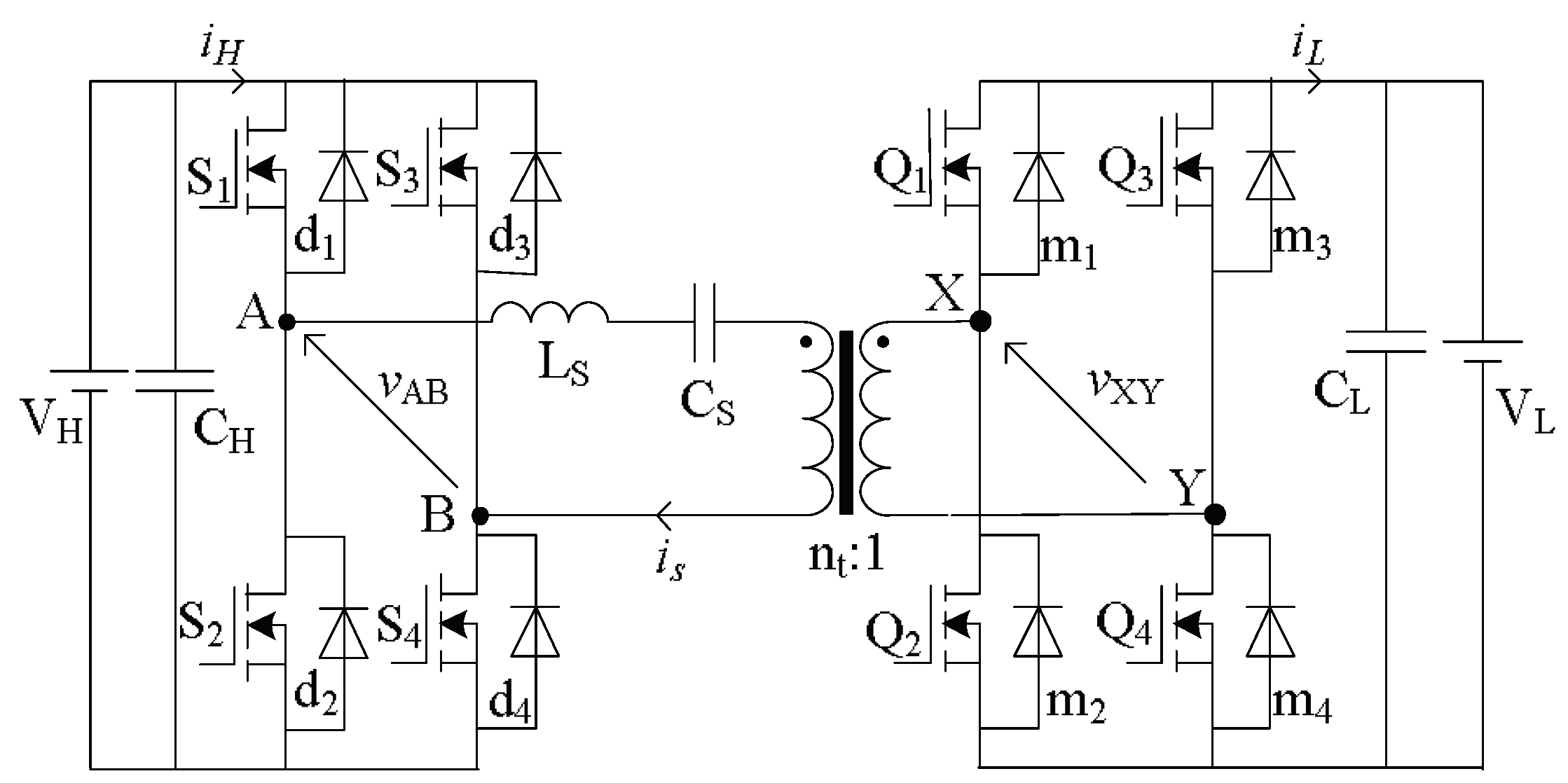
2. Steady-State Analysis for DBSRC with DPS Control

As shown in Figure 2, a dual-bridge series resonant converter consists of two full-bridges, which are linked by a series LC-type resonant tank and a high-frequency (HF) isolation transformer. The two voltage sources V H and V L are high-voltage (HV) side voltage and low-voltage (LV) side voltage, respectively. S 1 S 4 and Q 1 Q 4 are eight MOSFET switches with body diodes. C H and C L are filter capacitors on the HV side and LV side, respectively.
In Figure 3, steady-state waveforms of the DBSRC with DPS modulation for two directional power transfers are presented. The power transfer from the HV side to the LV side is defined as a positive power. All switches in each bridge arm are operating alternatively at almost 50% duty cycle with necessary deadband. The bidirectional power is a function of two phase-shift angles. The inner-bridge angle α 1 is defined as the phase-shift by which the gating signal of S 4 leads to that of S 1 , which is in the range of [0, π ]. The inter-bridge angle α 2 is defined as the phase-shift by which the gating signal of S 1 leads to that of Q 1 . The range of α 2 depends on the polarity of power and the value of α 1 . Consequently, the HF AC voltage on the HV side v A B is a quasi-square wave voltage with a variable pulse width ( π α 1 2 ), while the LV side HF AC voltage v X Y is a square wave voltage. The angle by which the fundamental component of v A B leads to the fundamental component of v X Y is defined as ϕ , which is always equal to ( α 1 / 2 + α 2 ) regardless of power transfer direction. β is the angle by which the fundamental component of v A B leads to the fundamental component of resonant current i s .
In this work, the fundamental harmonics approximation (FHA) approach is utilized for the steady-state analysis as the converter is designed to work nearly at the resonance state. The obtained results can be used for a quick initial design. In this paper, the LV side voltage V L is assumed in the range of V L m i n V L m a x and the HV side voltage V H is fixed. For the purpose of simplicity, all quantities refer to the HV side (marked by a superscript “ ” if the quantity is on the LV side actually) and normalized by the following base values:
V B = V H , Z B = n t 2 V L m a x 2 P F , I B = V B Z B , f B = 1 2 π L s C s
where f B is the resonance frequency, P F is the rated full-load power, and n t is the HV-to-LV turn ratio of the HF transformer.
The voltage gain of the bidirectional converter is defined as:
M = n t V L V H
All normalized reactance can be expressed as:
X L s , p u = Q F ; X C s , p u = Q / F ; X s , p u = X L s , p u + X C s , p u = Q ( F 1 / F )
where the quality factor Q is defined as Q = 2 π f B L s Z B = 1 2 π f B C s Z B , normalized switching frequency F is F = f s / f B , and f s is the switching frequency.
The equivalent circuit of a DBSRC in steady-state is given in Figure 4. According to the waveforms of v A B and v X Y shown in Figure 3, the normalized fundamental components of the two voltage sources can be calculated as:
v A B , 1 p u ( ω s t ) = 4 π cos ( α 1 2 ) sin ( ω s t )
v X Y , 1 p u ( ω s t ) = 4 M π sin ( ω s t ϕ )
By using the principle of superposition, the normalized fundamental resonant current i s , pu can be found easily as:
i s , p u ( ω s t ) = 4 [ M cos ( ω s t ϕ ) cos ( α 1 2 ) cos ω s t ] π X s , p u
The normalized peak current I s p , p u is given as:
I s p , p u = 4 M 2 2 M L cos ( ϕ ) cos α 1 2 + cos 2 α 1 2 π X s , p u
The necessary conditions of ZVS operation for all switches require that the anti-parallel diodes be turned on prior to the switch channel. These conditions could be checked by evaluating the resonant current at three special time points, which are the turn-on moment of S 1 , the turn-on moment of S 3 , and the turn-on moment of Q 1 , Q 4 , respectively. The three instantaneous values of resonant current should satisfy the following inequality:
i s , p u ( α 1 2 ) = 4 [ M cos α 2 cos 2 ( α 1 2 ) ] π X s , p u < 0
i s , p u ( π α 1 2 ) = 4 [ cos 2 ( α 1 2 ) M cos ( α 1 + α 2 ) ] π X s , p u > 0
i s , p u ( α 1 2 + α 2 ) = 4 ( M cos α 1 2 cos ϕ ) π X s , p u < 0
After simplification, the following results are obtained.
M cos α 2 < cos 2 α 1 2
M cos ( α 1 + α 2 ) < cos 2 α 1 2
M > cos α 1 2 cos ϕ
The three inequality expressions are necessary ZVS conditions for S 1 , S 2 , ( S 3 , S 4 ), and ( Q 1 Q 4 ), respectively. The statements above are valid for both positive and negative power.
According to the discussion above, the relationship between the soft-switching conditions and the voltage gain of the converter are illustrated in Figure 5a–c. In each figure, the two straight solid lines indicate the boundary of α 2 . The ZCSoperation region is enclosed by the curves, whose area depends on the voltage gain.
The average power transferred between the two DC sources can be evaluated as:
P o , p u = 8 M π 2 Q ( F 1 F ) cos α 1 2 sin ( α 1 2 + α 2 )
Apparently, the polarity of transferred average power relies on the polarity of sin ( α 1 2 + α 2 ) . Therefore, if the power is positive, α 2 is in the range of [ α 1 2 , π α 1 2 ] . If the power is negative, α 2 is in the range of [ π α 1 2 , α 1 2 ] . The normalized power can also be expressed as:
P o , p u = P V B 2 / Z B = P P F ( n t V L m a x V B ) 2 = G M m a x 2
where G = P P F [ 0 1 ] is the percentage of the power level and M m a x = n t V L m a x V H is the maximum voltage gain. Substituting (15) into (14) yields:
M m a x 2 M = 8 π 2 G Q ( F 1 F ) cos α 1 2 sin ( α 1 2 + α 2 )
This equation above describes the relationship among the power level (G) and the varying voltage gain M in a DBSRC under DPS modulation. If either or both of the two quantities ( G , M ) changes, the two phase-shift angles shall be adjusted appropriately to keep the balance in (16).

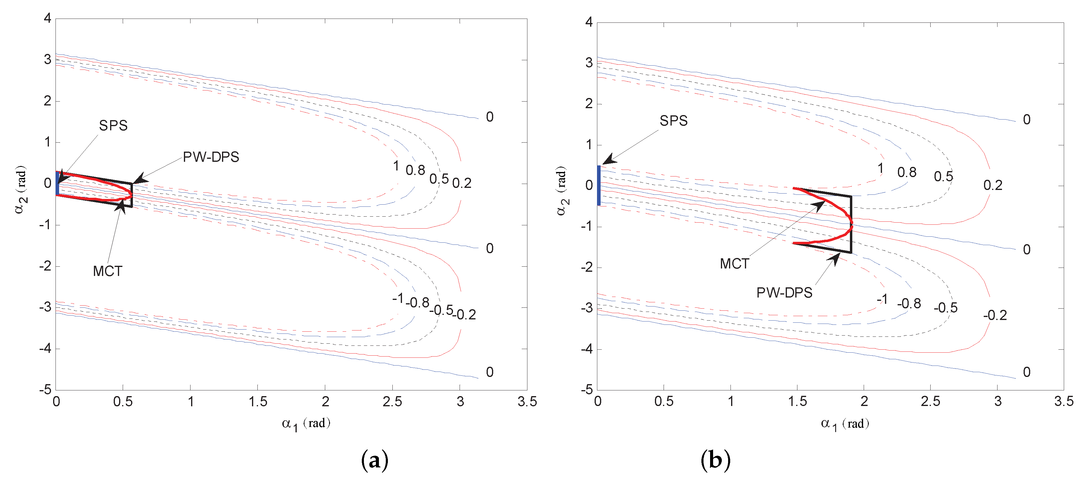
3. The Proposed Piecewise Control Strategy

3.1. Design Approach

According to (14) and (16), there are infinite combinations of α 1 and α 2 that are able to achieve a particular voltage gain at a particular power, in theory. In this work, the top priority for selecting a suitable control strategy is to reduce circulation energy and, meanwhile, to maintain a wide ZVS operation range with the variation of both the load and the converter gain. Inspired by the fact that a unity converter gain M is the optimal situation for ZVS operation when SPS control is adopted, a piecewise control strategy based on DPS is proposed.
At first, the principles of the piecewise control strategy can be summarized as:
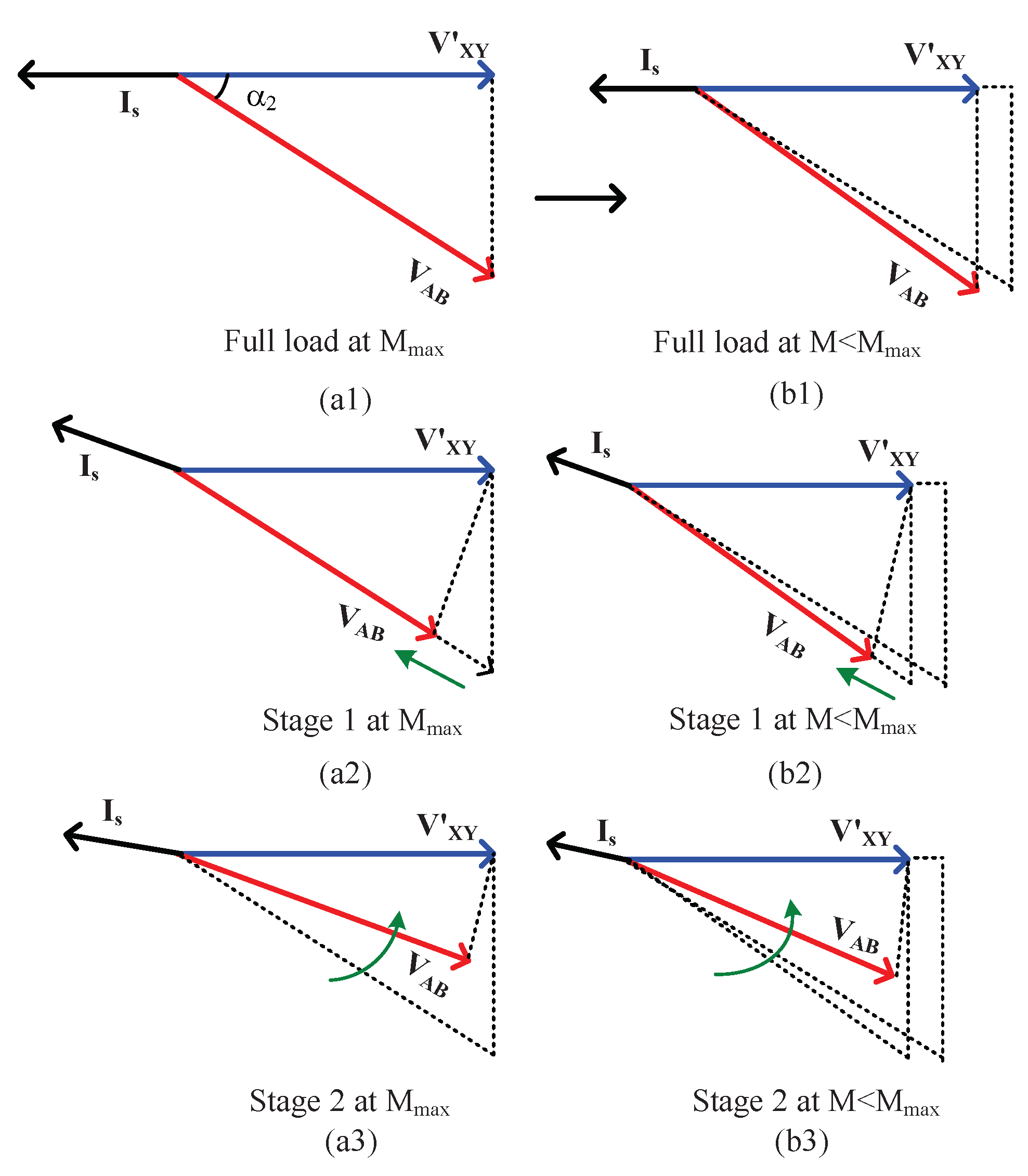
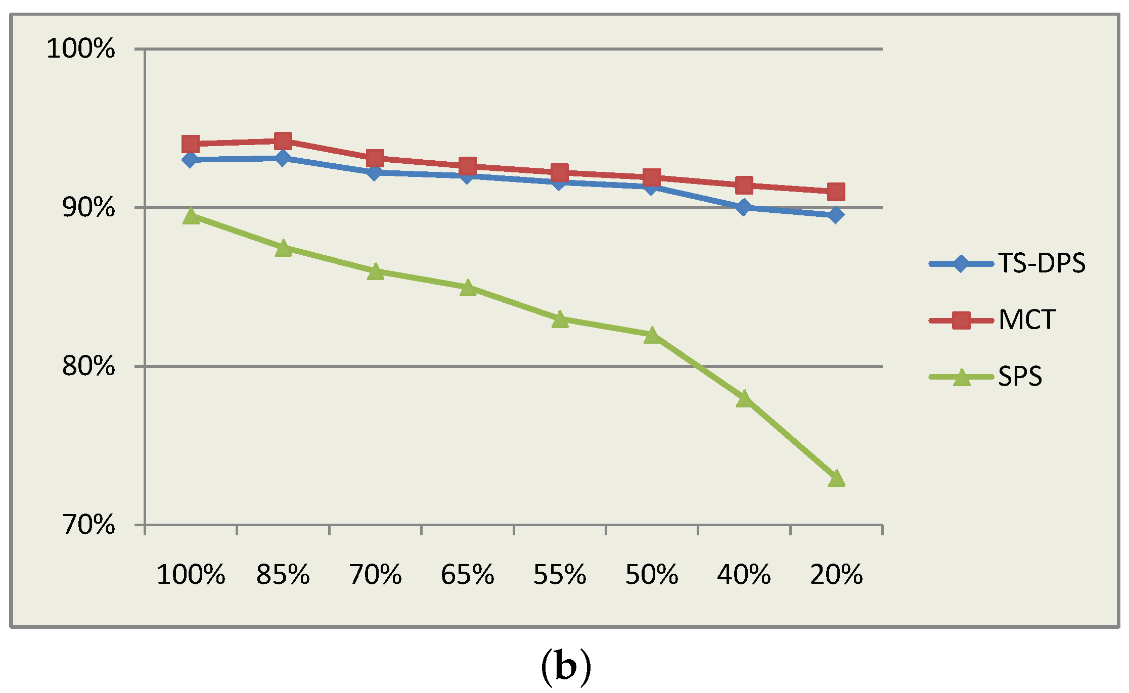
  • The high circulation current would induce high rms current and hence result in high conduction loss, especially on low-voltage high-current side at heavy load. Therefore, the LV-side voltage and current are manipulated to be in phase (i.e., zero circulation energy) at full load regardless of the converter gain and the polarity of power. At this moment, the power factor on the LV side is unity, and the power factor on the HV side has the minimum value.
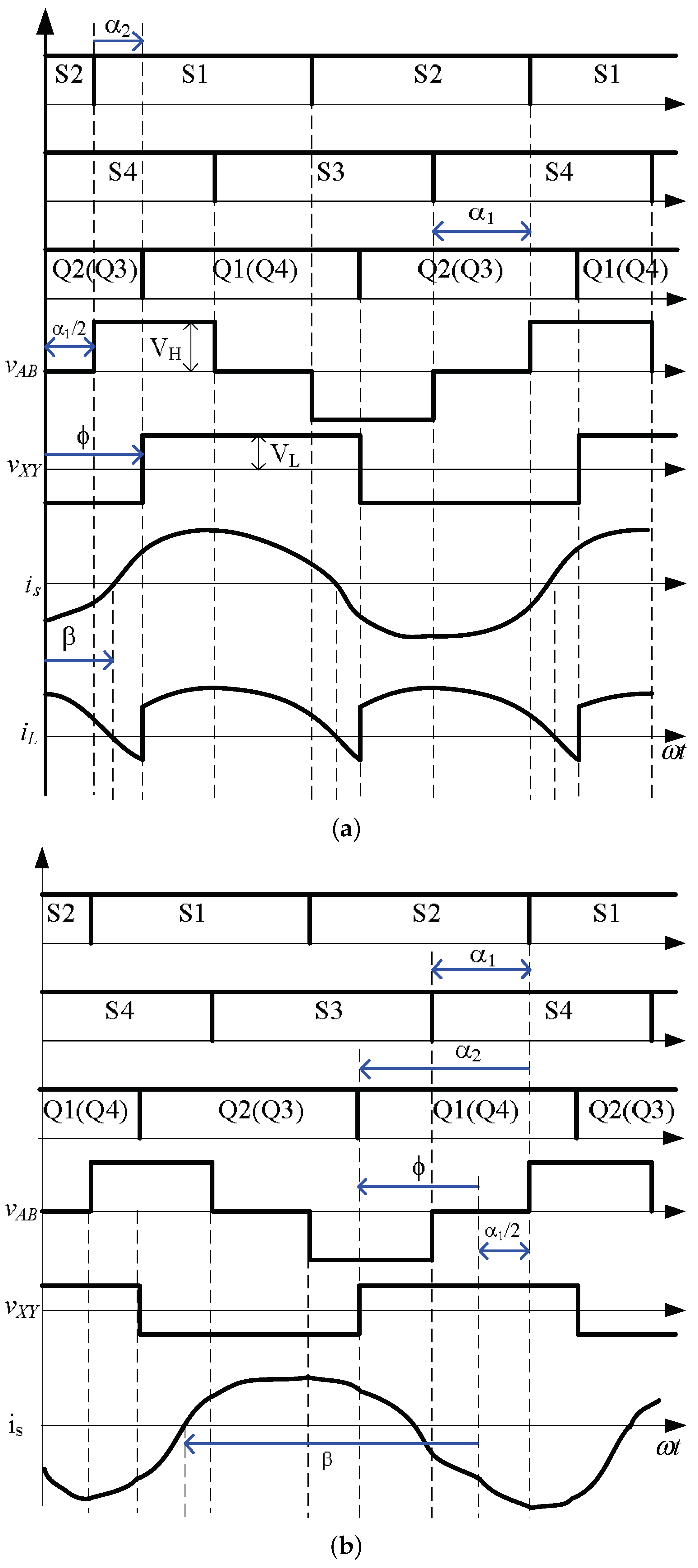
  • Phase I, heavy load: At a reduced load level, the pulse-width of the HV-side HF AC voltage ( v A B ) is reduced until the length of effective HV-side AC voltage vector V AB has the same length as that of the LV-side HF AC voltage vector V XY . In Phase I, the power factor on the LV side decreases and the power factor on the HV side increases.
  • Phase II, light load: To achieve even a low load level, the angle between two isometric voltage vectors ( V AB and V XY ) is reduced, which is actually analogous to the unity gain operation of DAB or DBSRC with SPS control. In Phase II, the power factor on both sides increases.
Based on the principle, the converter operation under the piecewise control strategy will be explained in detail for the case of positive power transfer. To make the explanation understandable, the phasor diagrams to illustrate key operation conditions for positive power are presented in Figure 6.

3.2. Full Load Operation

3.2.1. Full Load Operation at M = M m a x

This special operation situation is used for the converter design with maximum power P F and the maximum voltage gain M m a x (i.e., V L = V L m a x ). At the design point shown in Figure 6a1, α 1 is equal to zero to let v A B have a maximum pulse width to make full use of the input. α 2 is chosen so that the resonant current vector I s is in phase with the phasor V XY , which means zero circulation current on the LV side. The two phase-shift angles at the design point are:
α 1 = 0 α 2 = arccos ( M m a x ) = ϕ o
where ϕ o is the inter-bridge phase-shift at the design point.
With above resonance operation ( F > 1 ), there is a certain amount of circulation current existing on the HV side at the design point. On the one hand, a small amount of circulation current is helpful to realize ZVS operation for the HV side bridge. On the other hand, a large amount of circulation current will increase rms current and bring up more conduction loss. Fortunately, the induced conduction loss is low since the current on the HV-side is relatively low. Furthermore, the loss can be reduced by a proper selection of M m a x .

3.2.2. Full Load Operation at
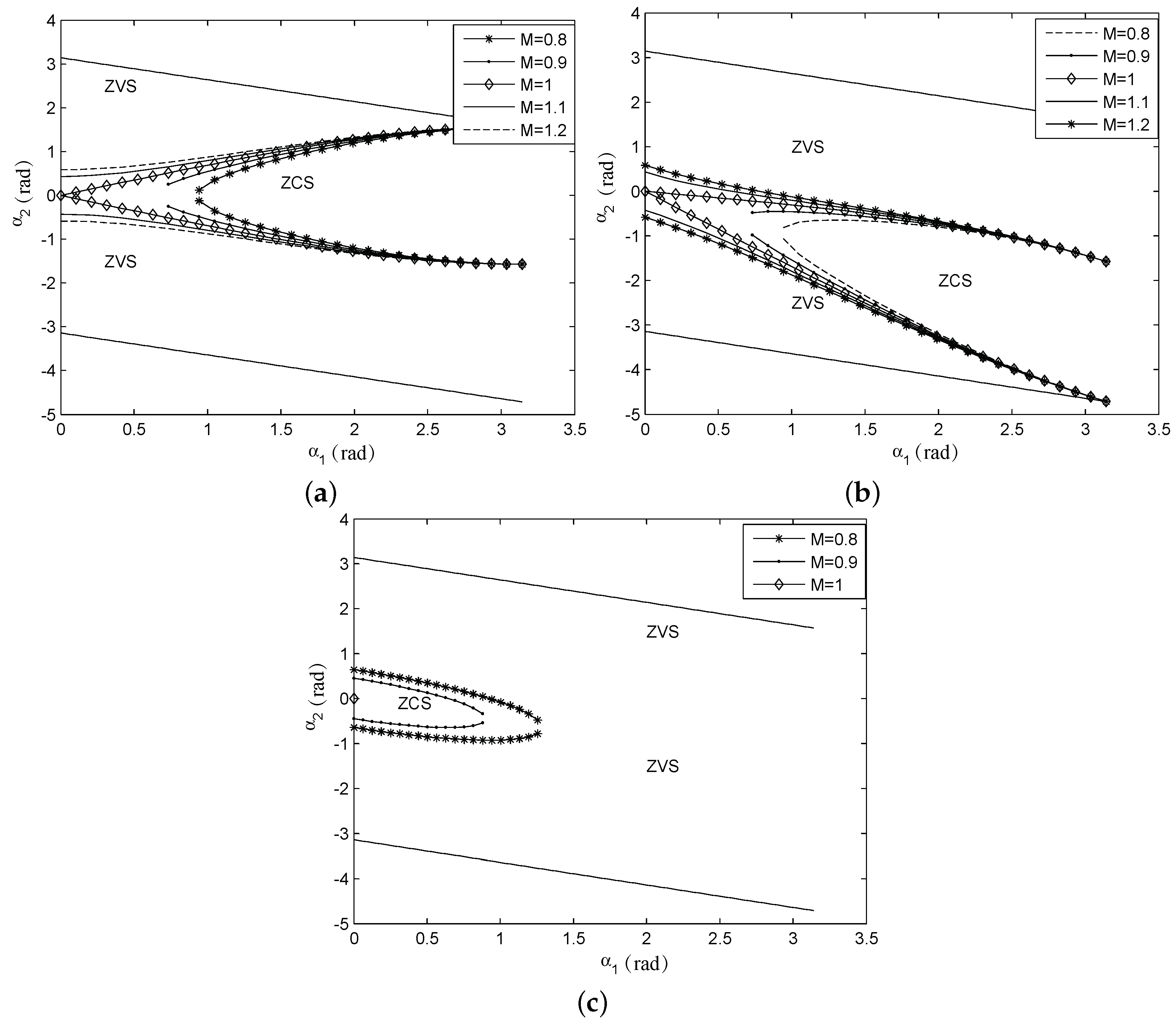
 M < M m a x

At full load operation with M < M m a x , a similar right-angle phasor triangle could be constructed to make the resonant current I s be in phase with V XY . Both α 1 and ( α 1 / 2 + α 2 ) have to be adjusted properly compared with the case at the design point. With a lower V L , the load current is higher than before at full load, i.e., the length of V XY is shorter and the length of I s (which is proportional to V AB V XY ) is longer compared with the case in Figure 6a1. At the full load condition with M < M max (Figure 6b1), the two phase-shift angles can be solved geometrically:
ϕ o * = arccos M 2 M 4 M max 4 + M max 2 α 1 = 2 arccos M 4 M max 4 + M max 2 M α 2 = ϕ o * α 1 2

3.3. Phase I

As shown in Figure 6b2, in order to regulate the output power in Phase I, α 1 is increased and α 2 is decreased, while the sum ( α 1 / 2 + α 2 ) is fixed at ϕ o * . The results in the phasor diagram are that the length of phasor V AB is shortened and the angle between the two voltage phasors is still equal to ϕ o . During the procedure, the circulation current on the HV side decreases and the circulation current on the LV side increases. Furthermore, the length of the resonant current phasor I s decreases.
α 1 = 2 arccos G M 4 M max 4 + M max 2 M α 2 = ϕ o * α 1 / 2
Phase I ends when the lengths of two voltage phasors are equal. At the boundary point, the power level is:
G b = cos ϕ o * = M 2 M 4 M max 4 + M max 2
and the two phase-shift angles are:
α 1 = 2 arccos M α 2 = ϕ o * α 1 / 2

3.4. Phase II

As shown in Figure 6b3, only α 2 is decreased to manipulate output voltage in Phase II. This is an imitation of DAB or DBRC with SPS at unity gain. The length of the resonant current phasor continues to decline, and the circulation current on both the HV side and the LV side decreases.
α 1 = 2 arccos M α 2 = arcsin G M max 1 M max 2 M 2 arccos M
In order to realize the case in Figure 6b1, there is a limit on the range of converter gain. The restriction of converter gain is given as:
M min 2 > 1 M max 2
For a converter with a voltage gain range that does not satisfy (23), it is impossible to achieve zero circulation energy at full load. If the power direction is reversed, the piecewise control strategy can be applied as well. It can be understood easily with the fundamental phasor diagram shown in Figure 7.

3.5. A Design Example

The following specifications are used in the paper to illustrate the design procedure: the HV-side voltage V H is 100 V; the LV-side voltage V L is 28.8–48 V; the rated power P F is 200 W; switching frequency f s is equal to 100 kHz. The design point is selected at the condition with M = M max (i.e., V H = 100 V, V L = 48 V) and the rated power. The approximately optimal parameters for designing a DBSRC can be chosen according to [10], then the voltage gain M and the normalized switching frequency F in this work are chosen as: M m a x = 0.96 , F = 1.1 .
According to the definition of converter gain, the HV-to-LV turn ratio of the HF transformer n t can be calculated:
n t = V B · M max V Lmax = 2 .
The impedance base value Z B is calculated as:
Z B = n t 2 V Lmax 2 P F = 46.08 Ω
At the design point, the load condition is G = 1 . By using (16), the quality factor is calculated as:
Q = 8 · sin α 2 π 2 · M · ( F 1 / F ) = 1.238
Therefore, the values of L s and C s are calculated as:
L s = Q F Z B 2 π f s = 99.87 μ H C s = F 2 π f s Q Z B = 30.69 n F
Results of some particular cases at M = M max and M = M min for both positive power and negative power are listed in Table 1. The calculation of two phase-shift angles can be done similarly with the help of (18)–(22) for other power levels and other voltage gains.
In Figure 8, the relationship between the output power and the phase-shifts for the design example are presented. The contours shown are the levels of normalized bidirectional power. The actual varying paths of the two phase shifts based on the SPS, PW-DPS, and MCT control strategy are all marked for bidirectional power with maximum gain (Figure 8a) and minimum gain (Figure 8b), respectively. Marked in black color, the control path of PW-DPS consists of two line sections. Aligned on the y-axis and marked in blue color, the control path of SPS control is a straight line as well, since α 1 is always kept at zero. Marked in red color, the control paths under MCT control is a piece of smooth curve, which is almost enclosed by the trajectory of PW-DPS. It can be shown that the MCT and PW-DPS share similar changing trends, even though they are not derived from the same approach.

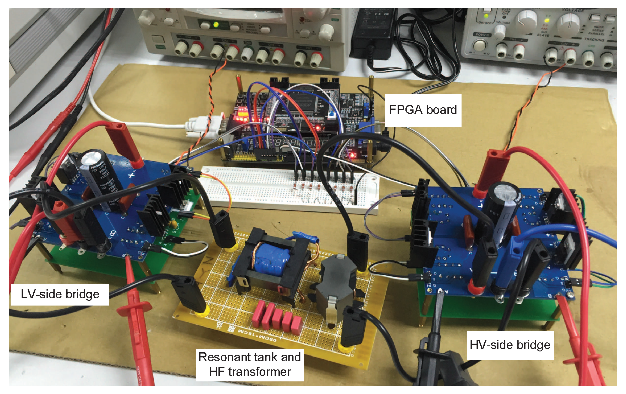
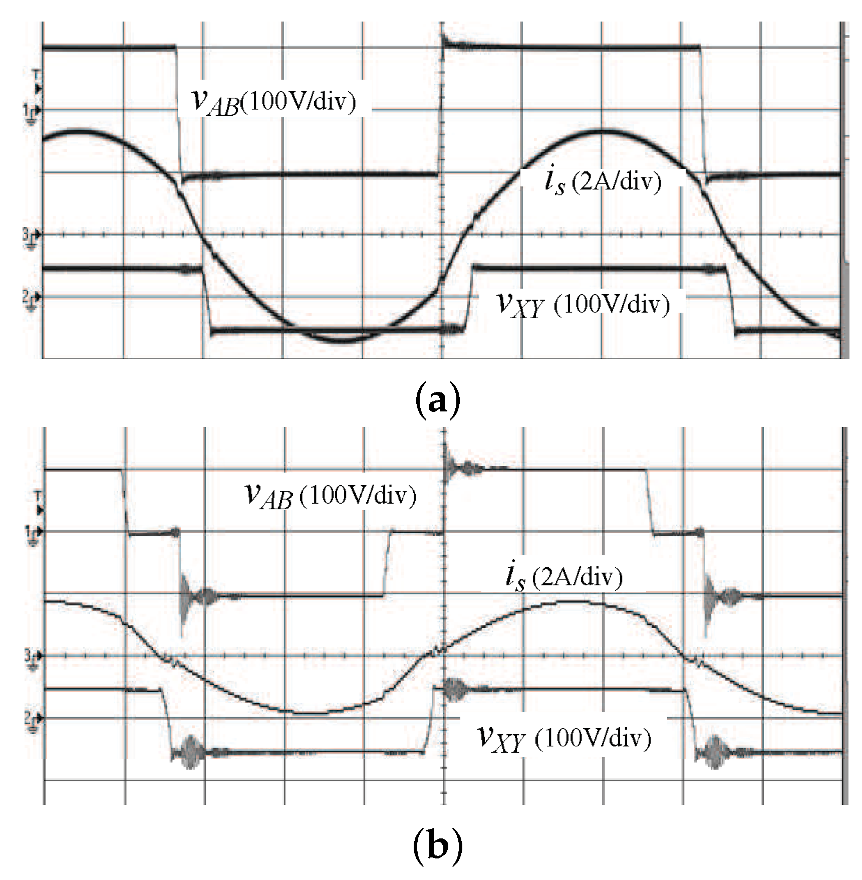
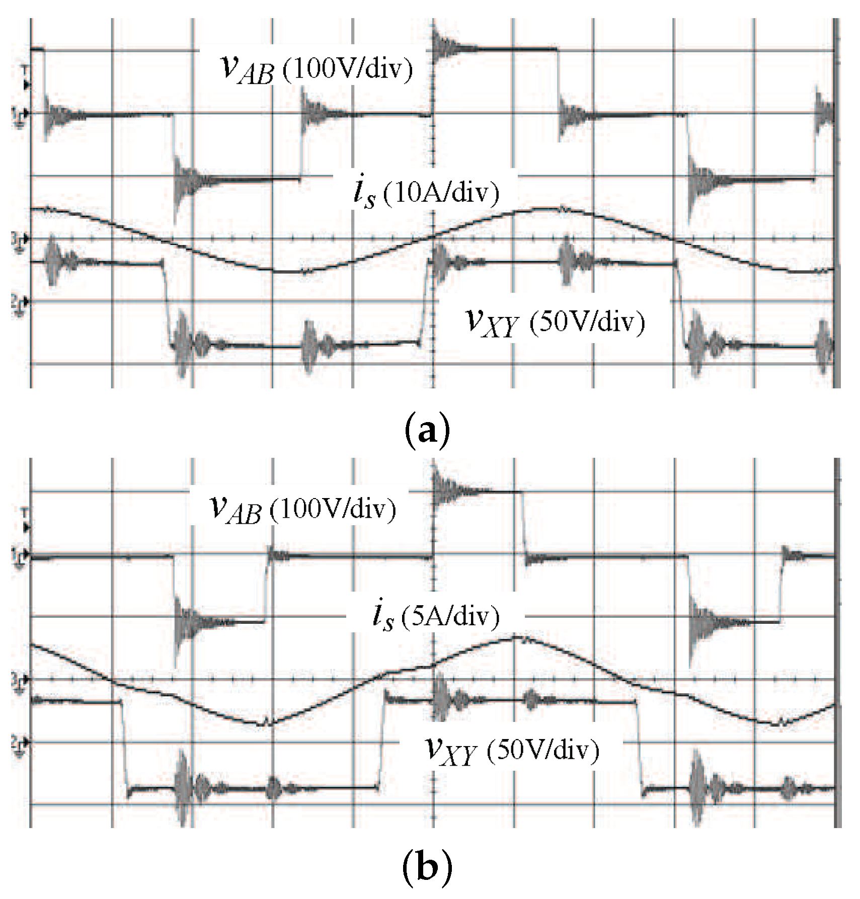
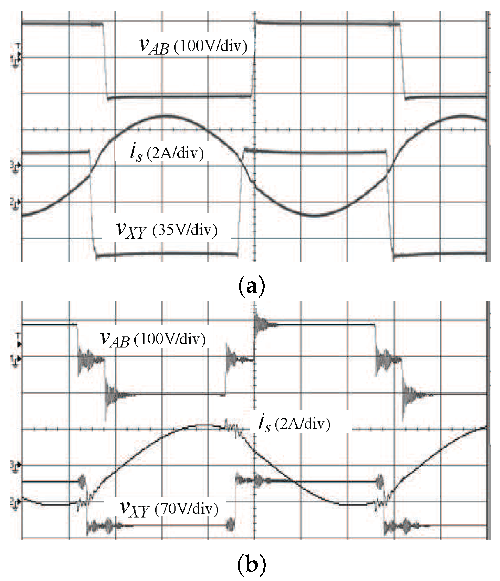
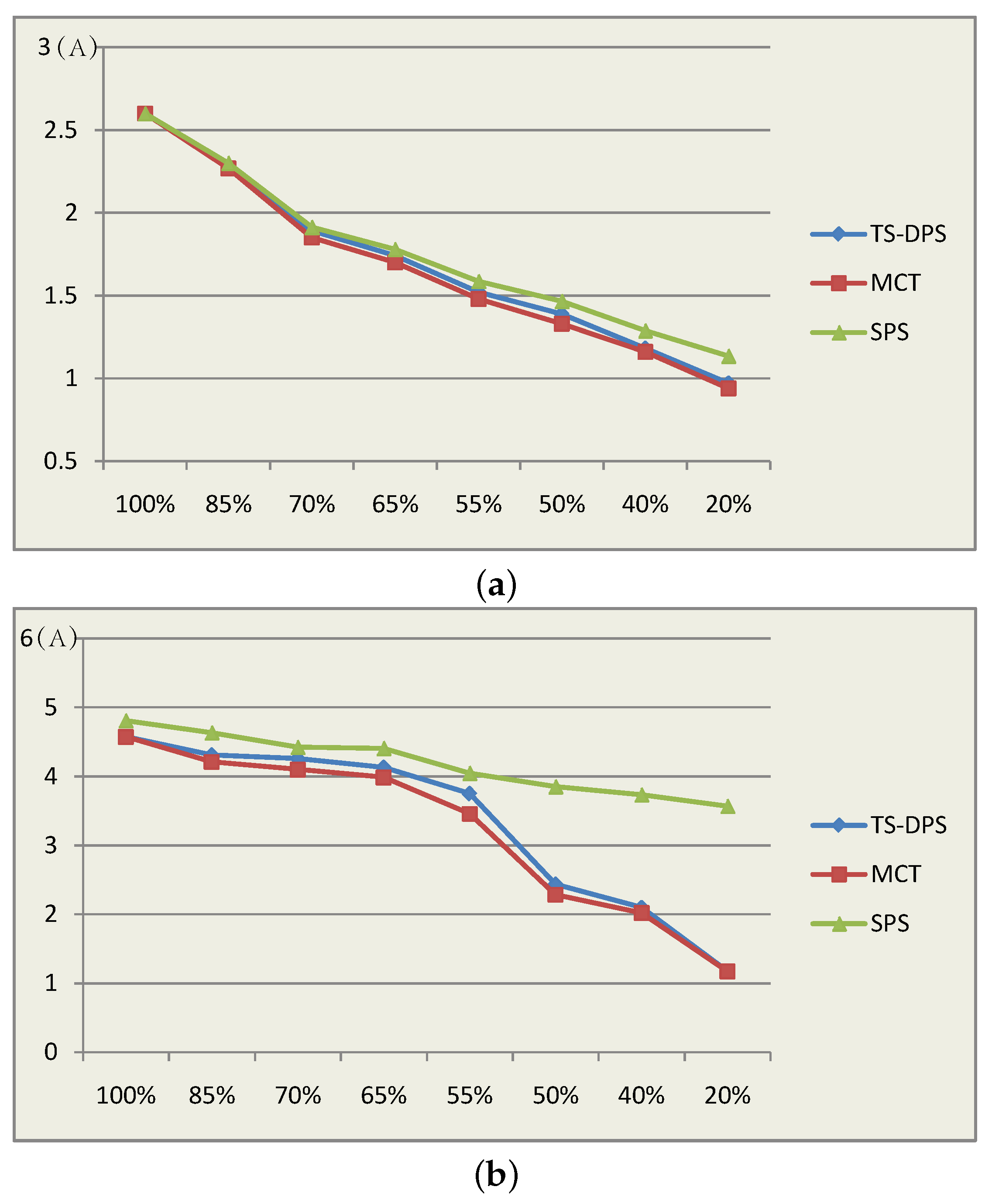
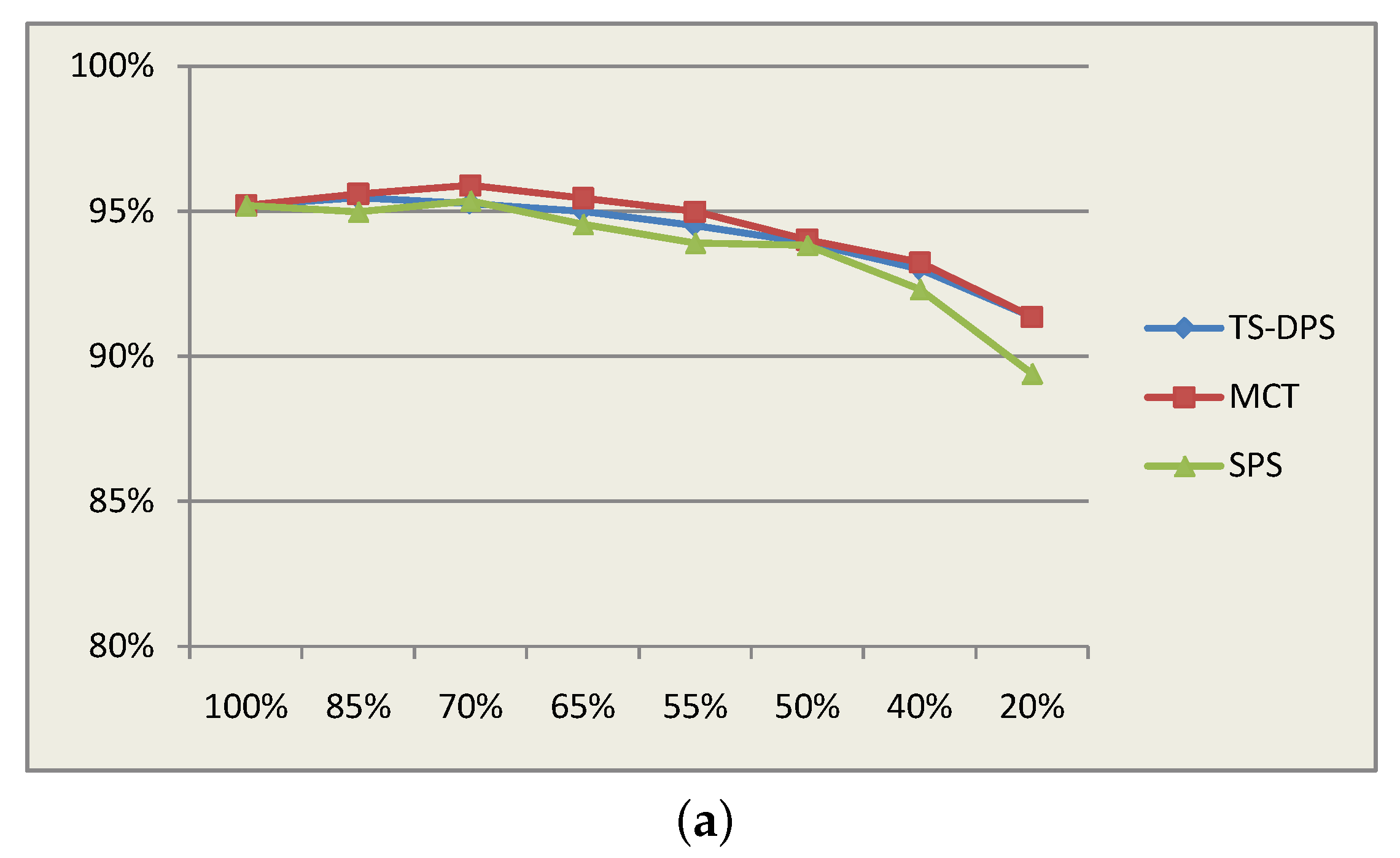
4. Verification with Simulation and Experimental Results

To verify the proposed PW-DPS control strategy, a series of simulations were performed in PSIM. The DBSRC to be tested has the same specification as designed in the last section. In order to get accurate results, the non-ideal parameters are assigned to the components in PSIM. The diode threshold voltage of power MOSFET is set to 1.3 V, and the on-state resistance of MOSFET is set to 0.06 Ω . To show the hard switching losses, the parasitic capacitor is set to 0.2 nF. Figure 9a–d presents some simulation plots, which were tested under the full load and half load operation at M max and M min , respectively, when the net power is positive. The same curves are illustrated for the reverse power flow in Figure 9e–h.
The waveforms recorded in the simulation include: v AB , v XY (two HF AC voltages), i s (the resonant current), i H , i L (the currents on both HV and LV side without filtering), i s 1 (switch current of the lagging arm in the HV-side bridge), i s 3 (switch current of the leading arm in the HV-side bridge), and i Q 1 (switch current in the LV-side bridge). It can be observed from the waveforms of i s and i Q 1 that the circulation current on the LV side is almost zero at full load test and also not significant at half load regardless of the converter gain and power direction, which indicates low conduction losses and high efficiency. The HV side current is discontinuous due to the PWM control except for the operation with full load and maximum converter gain. As for soft-switching conditions, the LV-side switches are able to be turned on/off with zero current under full load condition for both M max and M min . For half-load test conditions, switches in the LV side are turned on with zero voltage, which can be determined from the waveforms of i Q 1 . According to the phase delay between v AB and i s or the waveforms of switch currents for positive power flow, switches in the leading arm of the HV side bridge can maintain ZVS, while switches in the lagging arm of the HV side bridge would lose ZVS at partial load. When the power flow is negative, the conditions are just opposite, i.e., switches in the lagging arm of the HV side bridge can maintain ZVS, while switches in the leading arm of the HV side bridge would lose ZVS at partial load.
A lab prototype of the DBSRC was built and tested, as well. Eight MOSFET IRFS4620 ( R d s = 63.7 m Ω ) were selected as the main switches. The HF transformer had two windings with an 18:9 turn ratio, which were wound on an ETD39 ferrite core (Material N97). The gating signals were generated from an FPGA board and sent to the IR2181-based driver circuit. The resonant inductor was made of an RM12 air-gapped ferrite core (Material 3C95) wound with nine turns of wire. The photo of the experimental setup is given in Figure 10. The oscilloscope used to measure the waveforms was the Agilent DSO-X 3024A. The voltage probe was the Agilent N2791A, 25-MHz differential probe with an attenuation ratio at 100:1. The current probe was the Agilent N2782B.
The signals measured in the experimental test were HF AC voltage v A B , v X Y , and resonant current i s . In general, the experimental waveforms had a good match with the simulation results. Figure 11 shows the operation condition when the load levels were 200 W and 100 W with V L = 48 V. The operation condition when the load levels were 200 W and 100 W with V L = 28.8 V are presented in Figure 12. Figure 13 and Figure 14 show the same conditions except for the reverse power flow. As predicted by theoretical calculation and simulation, the circulation current on the LV side in the experimental plots is quite low from full load to partial load. ZVS transition can be observed from the soft rising/falling edges of v A B and v X Y . In the theoretical calculation, the magnetizing inductance of the HF transformer is neglected. In the actual implementation, the magnetizing inductance may be helpful to maintain ZVS for switches on the LV side, especially at partial load.
For the sake of a fair comparison, the prototype converter was also tested with SPS and MCT control. In Figure 15, the comparisons of the variation of rms resonant current with regards to load level under SPS, MCT, and PW-DPS control are presented for different voltage gains, respectively. It can be seen that there were no significant differences for those three controls when the converter gain was maximum. This can be attributed to the approximated optimal circuit design for maximum converter gain. When the converter gain was away from the designed one, the MCT and PW-DPS still had similar performance, and they showed apparent advantageous over the conventional SPS control, i.e., low rms resonant current, which indicates that the proposed control can provide lower loss and higher efficiency. The measured efficiency of the lab prototype converter under different control schemes is listed in Figure 16 for comparison. It can be shown that both MCT and PW-DPS control were able to maintain relatively high efficiency among a wide range of load levels, while the SPS control had weak performance when the voltage gain was away form the designed value. Being claimed as the minimized current control, MCT control did show better performance over the proposed PW-DPS control; however, the margin was not large. The potential reasons might be: (1) the proposed control happened to be a good piecewise approximation of the MCT, though no minimization calculation was executed; (2) the MCT calculation was also based on the FHA approach, which is known to have limited accuracy, especially at a low load level.

5. Conclusions

To improve the performance of a dual-bridge series resonant converter, a piecewise control strategy based on dual-phase-shift modulation is proposed in this work. This PW-DPS control tends to achieve a compromise between the flexibility and simplicity of control by using only two phase-shift angles. By properly adjusting the two phase-shift angles in two phases, there is no circulation current existing on the low-voltage/high-current side at full load regardless of the power direction and variation of the LV-side voltage. Compared with SPS control, it is found that the proposed control strategy is able to alleviate circulation energy significantly, reduce conduction loss and maintain high efficiency over a wide range of load levels and LV-side voltage. Besides, at least six out of eight switches in the converter can be turned on with ZVS for the whole operation range. Although not derived for the objective to optimize the rms resonant current, the proposed PW-DPS control demonstrates competitive performance compared with the optimized MCT control in terms of rms resonant current and efficiency in a series of experimental tests. The calculation used in PW-DPS control is also simpler than that in MCT control. The number of control variables isless than that of MCT control. Besides, it is not difficult to implement the proposed PW-DPS control in a closed-loop manner. As shown in Equations (18)∼(22), the only parameter that needs to be monitored continuously is the LV-side voltage V L , which can be used to determine the actual voltage gain and the corresponding boundary load level G b according to (20). Through comparison between the load level command and the boundary load level, the control phase can be determined, and then, the appropriate formula (either (19) or (22)) can be selected to find the correct phase-shift angles. The dynamics and implementation of closed-loop control using PW-DPS deserve more efforts in future work. Using a DBSRC with the proposed PW-DPS with a much higher power rating, the performance of low-load operation might be poor due to the loss of ZVS. These drawbacks also need to be investigated further in the future.

Author Contributions

Conceptualization, X.L.; data curation, S.H.; formal analysis, S.-Z.Z.; funding acquisition, X.L.; investigation, S.-Z.Z.; methodology, S.-Z.Z.; project administration, X.L.; software, G.C.; supervision, X.L.; validation, S.-Z.Z. and G.C.; visualization, S.H.; writing, original draft, S.-Z.Z.; writing, review and editing, X.L. and S.H.

Funding

This work was supported by Fundo para o Desenvolvimento das Ci e ^ ncias e da Tecnologia under Grant No. 004/2015/A1.

Conflicts of Interest

The authors declare no conflict of interest.

References

  1. Blaabjerg, F.; Liserre, M.; Ma, K. Power electronics converters for wind turbine systems. IEEE Trans. Ind. Appl. 2012, 4, 708–719. [Google Scholar] [CrossRef]
  2. Bose, B. Global energy scenario and impact of power electronics in 21st century. IEEE Trans. Ind. Electron. 2013, 60, 2638–2651. [Google Scholar] [CrossRef]
  3. Park, J.; Choi, S. Design and control of a bidirectional resonant DC-DC converter for automotive engine/battery hybrid power generators. IEEE Trans. Power Electron. 2014, 29, 3748–3757. [Google Scholar] [CrossRef]
  4. Rathore, A.K.; Devendra, R.P.; Srinivasan, D. Non-isolated Bidirectional Soft-Switching Current-Fed LCL Resonant DC/DC Converter to Interface Energy Storage in DC Microgrid. IEEE Trans. Ind. Appl. 2016, 52, 1711–1722. [Google Scholar] [CrossRef]
  5. Chiu, H.J.; Lin, L.W. A bidirectional DC-DC converter for fuel cell electric vehicle driving system. IEEE Trans. Power Electron. 2006, 21, 950–958. [Google Scholar] [CrossRef]
  6. Rathore, A.K.; Prasanna, U.R. Analysis, design, and experimental results of novel snubberless bidirectional naturally clamped ZCS/ZVS current-fed half-bridge DC/DC converter for fuel cell vehicles. IEEE Trans. Ind. Electron. 2013, 60, 4482–4491. [Google Scholar] [CrossRef]
  7. Bal, S.; Rathore, A.K.; Srinivasan, D. Naturally Clamped Snubberless Soft-Switching Bidirectional Current-Fed Three-Phase Push-Pull DC/DC Converter for DC Microgrid Application. IEEE Trans. Ind. Appl. 2016, 52, 1577–1587. [Google Scholar] [CrossRef]
  8. Pan, X.; Rathore, A.K.; Prasanna, U.R. Novel soft-switching snubberless naturally clamped current-fed full-bridge front-end-converter-based bidirectional inverter for renewables, microgrid, and UPS applications. IEEE Trans. Ind. Appl. 2014, 50, 4132–4141. [Google Scholar]
  9. Jain, M.; Daniele, M.; Jain, P.K. A bidirectional DC-DC converter topology for low power application. IEEE Trans. Power Electron. 2000, 15, 595–606. [Google Scholar] [CrossRef]
  10. Li, X.; Bhat, A.K.S. Analysis and Design of High-Frequency Isolated Dual-Bridge Series Resonant DC/DC Converter. IEEE Trans. Power Electron. 2010, 21, 850–862. [Google Scholar]
  11. Chen, H.; Bhat, A.K.S. Analysis and design of a dual-bridge series resonant DC-to-DC converter for capacitor semi-active battery-ultracapacitor hybrid storage system. In Proceedings of the IEEE 23rd International Symposium on Industrial Electronics (ISIE), Istanbul, Turkey, 1–4 June 2014; pp. 1788–1793. [Google Scholar]
  12. Xiao, H.; Xie, S. A ZVS Bidirectional DC-DC Converter with Phase-Shift Plus PWM Control Scheme. IEEE Trans. Power Electron. 2008, 23, 813–823. [Google Scholar] [CrossRef]
  13. Li, X.; Li, Y.-F. An Optimized Phase-Shift Modulation for Fast Transient Response in a Dual-Active-Bridge Converter. IEEE Trans. Power Electron. 2014, 29, 2661–2665. [Google Scholar] [CrossRef]
  14. Sun, C.; Li, X.; Zhou, S.Z. Transient current control for a step load change in a dual-active-bridge converter. Electron. Lett. 2018, 54, 1290–1292. [Google Scholar] [CrossRef]
  15. De Doncker, R.W.; Divan, D.M.; Kheraluwala, M.H. A three-phase soft-switched high power density DC/DC converter for high power applications. IEEE Trans. Ind. Appl. 1991, 27, 63–73. [Google Scholar] [CrossRef]
  16. Kheraluwala, M.H.; Gascoigne, R.; Divan, D.M.; Baumann, E. Performance characterization of a high power dual active bridge DC-to-DC converter. IEEE Trans. Ind. Appl. 1992, 28, 1294–1301. [Google Scholar] [CrossRef]
  17. Sun, C.; Li, X. Fast transient modulation for a step load change in a dual-active-bridge converter with extended-phase-shift control. Energies 2018, 11, 1569. [Google Scholar] [CrossRef]
  18. Inoue, S.; Akagi, H. A bidirectional isolated DC-DC converter as a core circuit of the next-generation medium-voltage power conversion system. IEEE Trans. Power Electron. 2007, 22, 535–542. [Google Scholar] [CrossRef]
  19. Bai, H.; Mi, C. Eliminate reactive power and increase system efficiency of isolated bidirectional dual-active-bridge DC-DC converters using novel dual-phase-shift Control. IEEE Trans. Power Electron. 2008, 23, 2905–2914. [Google Scholar] [CrossRef]
  20. Zhao, B.; Song, Q.; Liu, W.; Sun, Y. Overview of Dual-Active-Bridge Isolated Bidirectional DC/DC Converter for High-Frequency-Link Power-Conversion System. IEEE Trans. Power Electron. 2014, 29, 4091–4106. [Google Scholar] [CrossRef]
  21. Inoue, S.; Akagi, H. A bidirectional DC-DC converter for an energy storage system with galvanic isolation. IEEE Trans. Power Electron. 2007, 22, 2299–2306. [Google Scholar] [CrossRef]
  22. Oggier, G.G.; Garcia, G.O.; Oliva, A.R. Switching Control Strategy to Minimize Dual Active Bridge Converter Losses. IEEE Trans. Power Electron. 2009, 24, 1826–1838. [Google Scholar] [CrossRef]
  23. Krismer, F.; Kolar, J.W. Closed Form Solution for Minimum Conduction Loss Modulation of DAB Converters. IEEE Trans. Power Electron. 2012, 27, 174–188. [Google Scholar] [CrossRef]
  24. Corradini, L.; Seltzer, D.; Bloomquist, D.; Zane, R.; Maksimovic, D.; Jacobson, B. Minimum current operation of bidirectional dual-bridge series resonant DC/DC converters. IEEE Trans. Power Electron. 2012, 27, 3266–3276. [Google Scholar] [CrossRef]
  25. Zhou, H.; Khambadkone, A.M. Hybrid Modulation for Dual-Active-Bridge Bidirectional Converter with Extended Power Range for Ultracapacitor Application. IEEE Trans. Ind. Appl. 2009, 45, 1434–1442. [Google Scholar] [CrossRef]
  26. Moonem, M.A.; Pechacek, C.L.; Hernandez, R.; Krishnaswami, H. Analysis of a multilevel dual active bridge (ml-dab) DC-DC converter using symmetric modulation. Electronics 2015, 4, 239–260. [Google Scholar] [CrossRef]
  27. Lu, M.; Li, X. Performance Evaluation of a Semi-Dual-Active-Bridge with PPWM Plus SPS Control. Electronics 2018, 7, 184. [Google Scholar] [CrossRef]
  28. Li, X.; Hu, S.; Sun, C.; Zhang, Y.F. Asymmetric-double-sided modulation for fast load transition in a semi-dual-active-bridge converter. IET Power Electron. 2017, 10, 1698–1704. [Google Scholar] [CrossRef]
  29. Qu, P.; Li, Z.; Wang, P.; Li, Y. Soft-switching study of high-frequency isolated dual-active-bridge resonant DC-DC converter considering harmonic components. In Proceedings of the IEEE Transportation Electrification Conference and Expo Asia-Pacific, Beijing, China, 31 August–3 September 2014; pp. 1–5. [Google Scholar]
  30. Li, X. A LLC-Type Dual-Bridge Resonant Converter: Analysis, Design, Simulation, and Experimental Results. IEEE Trans. Power Electron. 2014, 29, 4313–4321. [Google Scholar] [CrossRef]
  31. Malan, W.L.; Vilathgamuwa, D.M.; Walker, G.R. Modeling and control of a resonant dual active bridge with a tuned CLLC network. IEEE Trans. Power Electron. 2016, 31, 7297–7310. [Google Scholar] [CrossRef]
  32. Zhang, Y.; Li, X.; Sun, C.; He, Z. Improved Step Load Response of a Dual-Active-Bridge DC-DC Converter. Electronics 2018, 7, 185. [Google Scholar] [CrossRef]
  33. Hu, S.; Li, X.; Bhat, A.K.S. Operation of a bidirectional series resonant converter with minimized tank current and wide zvs range. IEEE Trans. Power Electron. 2019, 34, 904–915. [Google Scholar] [CrossRef]
Figure 1. A hybrid renewable energy generation system equipped with ESS.
Electronics 07 00374 g001
Figure 2. A dual-bridge series resonant converter.
Electronics 07 00374 g002
Figure 3. Typical steady-state waveforms of a dual-bridge series resonant converter (DBSRC) with dual-phase-shift (DPS) control for (a) positive power and (b) negative power flow.
Electronics 07 00374 g003
Figure 4. Equivalent circuit for steady-state analysis using fundamental harmonics approximation (FHA).
Electronics 07 00374 g004
Figure 5. Soft-switching conditions of switches (a) S 1 , S 2 , (b) S 3 , S 4 , and (c) Q 1 , Q 2 , Q 3 , Q 4 with regards to the two phase-shifts and the voltage gain M. ZVS, zero-voltage switching.
Electronics 07 00374 g005
Figure 6. Phasor diagram of the DBSRC with the piecewise dual-phase-shift (PW-DPS) control strategy for positive power flow.
Electronics 07 00374 g006
Figure 7. Phasor diagram of the DBSRC with the PW-DPS control strategy for negative power flow.
Electronics 07 00374 g007
Figure 8. The normalized bidirectional power with regards to the controlled phase-shift angles under single-phase-shift (SPS), minimum current trajectory (MCT), and PW-DPS control at (a) M = 0.96 and (b) M = 0.576 .
Electronics 07 00374 g008
Figure 9. Simulation plots at V H = 100 V and: (a) V L = 48 V, output power P o = 200 W; (b) V L = 48 V, output power P o = 100 W; (c) V L = 28.8 V, output power P o = 200 W; (d) V L = 28.8 V, output power P o = 100 W; (e) V L = 48 V, output power P o = −200 W; (f) V L = 48 V, output power P o = −100 W; (g) V L = 28.8 V, output power P o = −200 W; (h) V L = 28.8 V, output power P o = −100 W.
Electronics 07 00374 g009
Figure 10. Experimental setup of the DBSRC. HV, high voltage; LV, low voltage.
Electronics 07 00374 g010
Figure 11. Experimental plots at V L = 48 V, output power: (a) P o = 200 W; (b) P o = 100 W. Time scale: 1.52 μ s/div.
Electronics 07 00374 g011
Figure 12. Experimental plots at V L = 28.8 V, output power: (a) P o = 200 W; (b) P o = 100 W. Time scale: 1.52 μ s/div.
Electronics 07 00374 g012
Figure 13. Experimental plots at V L = 48 V, output power: (a) P o = −200 W; (b) P o = −100 W. Time scale: 1.52 μ s/div.
Electronics 07 00374 g013
Figure 14. Experimental plots at V L = 28.8 V, output power: (a) P o = −200 W; (b) P o = −100 W. Time scale: 1.52 μ s/div.
Electronics 07 00374 g014
Figure 15. Comparison of the measured rms resonant current under different load levels under SPS, PW-DPS, and MCT control: (a) M = 0.96 ; (b) M = 0.576 .
Electronics 07 00374 g015
Figure 16. Comparison of the measured efficiency of the DBSRC under different control schemes: (a) M = 0.96 ; (b) M = 0.576 .
Electronics 07 00374 g016aElectronics 07 00374 g016b
Table 1. Phase-shift angles under PW-DPS control for bidirectional power transfer.
Power α 1 α 2
200 W0 16.3 full load @ V L = 48 V
192 W32.6 0 boundary @ V L = 48 V
−200 W0 −16.3 full load @ V L = 48 V
−192 W32.6 −32.6 boundary @ V L = 48 V
200 W84.4 −3.2 full load @ V L = 28.8 V
155 W109.6 −15.8 boundary @ V L = 28.8 V
−200 W84.4 −81.2 full load @ V L = 28.8 V
−155 W109.6 −93.8 boundary @ V L = 28.8 V

