Abstract
As one of the most commonly used devices in microwave systems, bandpass filters (BPFs) directly affect the performance of these systems. Among the processes for manufacturing filters, integrated passive device (IPD) technology provides high practicality and accuracy. Thus, to comply with latest development trends, a resonator-based bandpass filter with a high selectivity and a compact size, fabricated on a gallium arsenide (GaAs) substrate is developed. An embedded capacitor is connected between the ends of two divisions in a circular spiral inductor, which is intertwined to reduce its size to 0.024 λg × 0.013 λg with minimal loss, and along with the capacitor, it generates a center frequency of 1.35 GHz. The strong coupling between the two ports of the filter results in high selectivity, to reduce noise interference. The insertion loss and return loss are 0.26 dB and 25.6 dB, respectively, thus facilitating accurate signal propagation. The filter was tested to verify its high performance in several aspects, and measurement results showed good agreement with the simulation results.
1. Introduction
The development of communication technology has resulted in the creation of many new microwave devices in the past decade, and has attracted public attention. Such devices have greatly improved our lives, and promoted the advancement of society. The widespread urban communication system requires a variety of components to transmit the required amounts of information. Thus, products such as amplifiers, mixers, baluns, and power dividers are being more extensively used. The proper operation of these complex systems demands filters to block unwanted noise and interference within selected frequency ranges. Bandpass filters (BPFs) are among the most essential components for applications on the microwave frequency bands, and their performances affect the operation of complete systems. As an electronic interface unit, the BPF allows the transmission of signals in a specific frequency range to reduce interference. Besides performance requirements, the increasingly complex structure and diverse uses of communication devices demand miniaturization to meet consumer expectations [1].
Different methods of designing BPFs have been proposed to meet diverse requirements. A common method consists of using parallel coupled lines or structures based on this classical prototyping [2,3], and its simplicity prevents high costs and provides devices with wide and flat passbands. Other methods adopt stub-loaded resonators for fabricating BPFs that are capable of controlling the resonant modes, thus easily enabling multiband response and control of the center frequency [4,5,6]. However, the length of the conventional transmission lines limits miniaturization when employing these methods. To overcome this shortcoming, several manufacturing processes have been proposed. Designs based on three-dimensional multilayer structures like liquid-crystalline polymer substrate [7] or low temperature co-fired ceramic technology [8] can greatly optimize the design, but they cannot be applied to mass production, given the high prices and large time consumption. Other designs use complementary metal-oxide-semiconductor transistor (CMOS) technology [9], and although it enables miniaturization, some parameters remain to be improved. For these reasons, integrated passive device (IPD) technology is preferred for designing microwave passive devices. IPD technology is a newly developed manufacturing technology that realizes an ideal integrated packaging system and provides complete module solutions at the same time. This technique can be used not only to process bandpass filters, lowpass filters or other filters, but also to process biosensors [10], power dividers [11], and couplers [12]. IPD technology can provide technical support for the growing chip market, with the help of its wide application in the processing of different devices.
In this study, we developed a compact on-chip BPF with a circular spiral inductor and an embedded capacitor. The filter is fabricated by using a gallium arsenide (GaAs) substrate at a center frequency of 1.35 GHz, and it was simulated by using a three-dimensional electromagnetic simulator for more accurate results. After analysis of the structure, we present the IPD process that is used to fabricate the filter. IPD technology allows for the simultaneous achievement of compact size, low cost, and excellent performance. In fact, the dimensions of the proposed BPF are 1.54 mm × 0.81 mm, which is ideal for the telecom industry, whose devices require a high degree of integration and accuracy. Moreover, we were able to generate circular patterns, which was relatively hard to process before, owing to inadequate processing techniques. Measurement results with an insertion loss of 0.26 dB and a return loss of 25.6 dB are provided and compared with results from similar works.
2. Materials and Methods
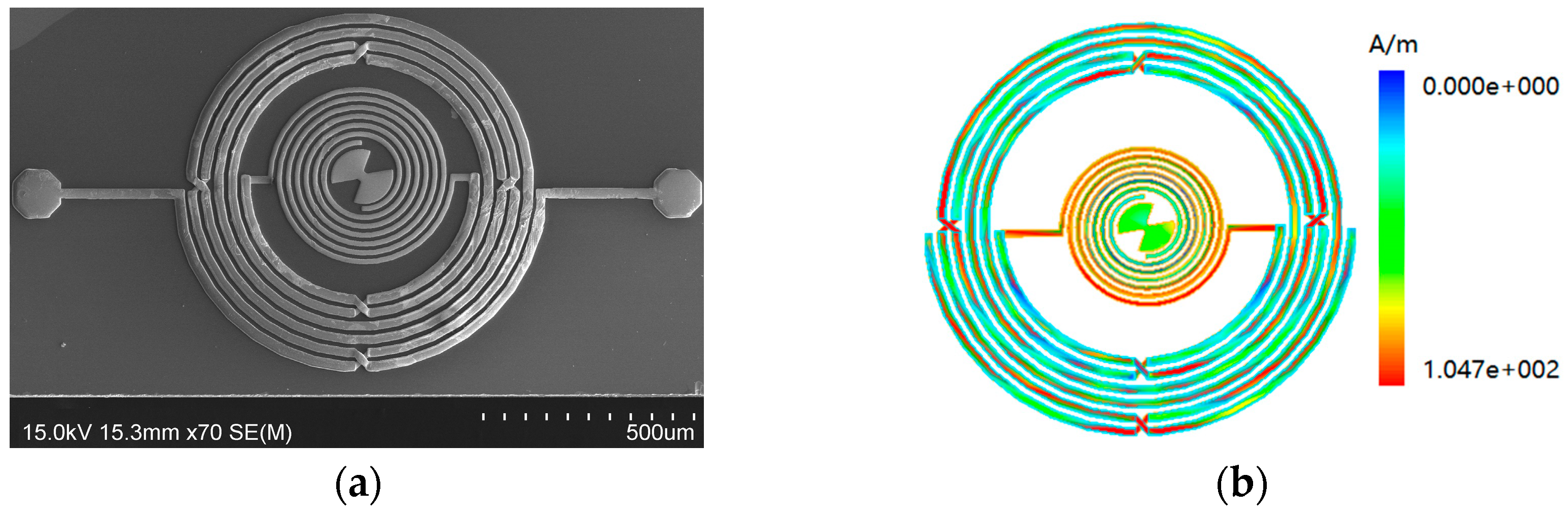
Many approaches are available for designing BPFs, from which the inductor-capacitor (LC) resonant structure employed in this study is easy to implement, compared to other methods, while providing the required effectiveness. The schematic of the proposed BPF is shown in Figure 1a, where the resonant frequency is mostly determined by the inductor and capacitor, which have circular shapes to allow the capacitor to be located exactly in the space between the two divisions of the inductor. The performance of the inductor is enhanced by mutual inductance from the intertwined and overlapped circular lines with air bridges. An air bridge is depicted in the enlarged view at the upper right corner of Figure 1a in four vertical directions. Five similar air-bridge structures are present in the proposed BPF, one at the upper side, two symmetrically located at the left and right sides, and the remaining two at the lower side. As depicted in the enlarged view at the bottom right corner of Figure 1a, r1 and r2 are the radii of the two small circles in the innermost ring of the embedded capacitor. A sector structure with a diameter of 100 µm in the middle can enhance coupling between the different parts. The line width and spacing of the outer ring are 20 µm and 14 µm, respectively, and both the line width and spacing of the inner ring are 10 µm. The combination of the left and right transmission lines can improve matching with the terminal, and current flows without distortion or interference by the elimination of excessive sharp turns that mitigates impedance loss.
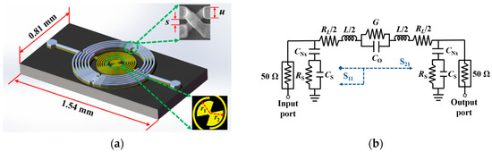
Figure 1.
Proposed bandpass filter (BPF): (a) layout (u = 20 μm, s = 14 μm); (b) equivalent circuit.
The exact realization of an ideal element is difficult. Neglecting some small values of feedthrough capacitance, the equivalent circuit of the proposed LC-type BPF is shown in Figure 1b. The model mainly consists of the inductor, capacitor, and its associated parasitic lumped elements. Variables RL and G denote the loss resistance and impedance in the inductor (L) and capacitor (CO), respectively, and CNx, CS, and RS represent the capacitance and resistance associated with the SiNx layer and the ground. The above parameters can be estimated as [13,14]:
where ρ is the resistance coefficient, l is the length of the circle, w is the metal width, δ is the skin depth in the conductor, t is the thickness of the conductor line, Csub and Gsub are the capacitance and conductivity per unit area of the GaAs substrate, respectively, and εNx and tNx are the dielectric constant and thickness of the SiNx layer for passivation, respectively. Although many factors affect the performance of the BPF, the center frequency is mainly determined by the circular spiral inductor and capacitor in the proposed design. The inductance of the circular inductor can be derived as in [15]:
with:
where μ is the magnetic permeability, n is the number of turns of the inductor, dA = 862 μm is the average diameter of the outer and inner ring of the inductor, and the value of η is approximately 0.22. The linear function between the capacitance of the concentric pattern and radius of the innermost circle can be used to obtain the capacitance. The capacitance value is solely determined by the material properties for a fixed width of the annular ring and the spacing between two adjacent rings [16,17]. Thus, a capacitor model that should be optimized through a simulation can be designed, because a capacitive effect exists between the metal layers and the ground.
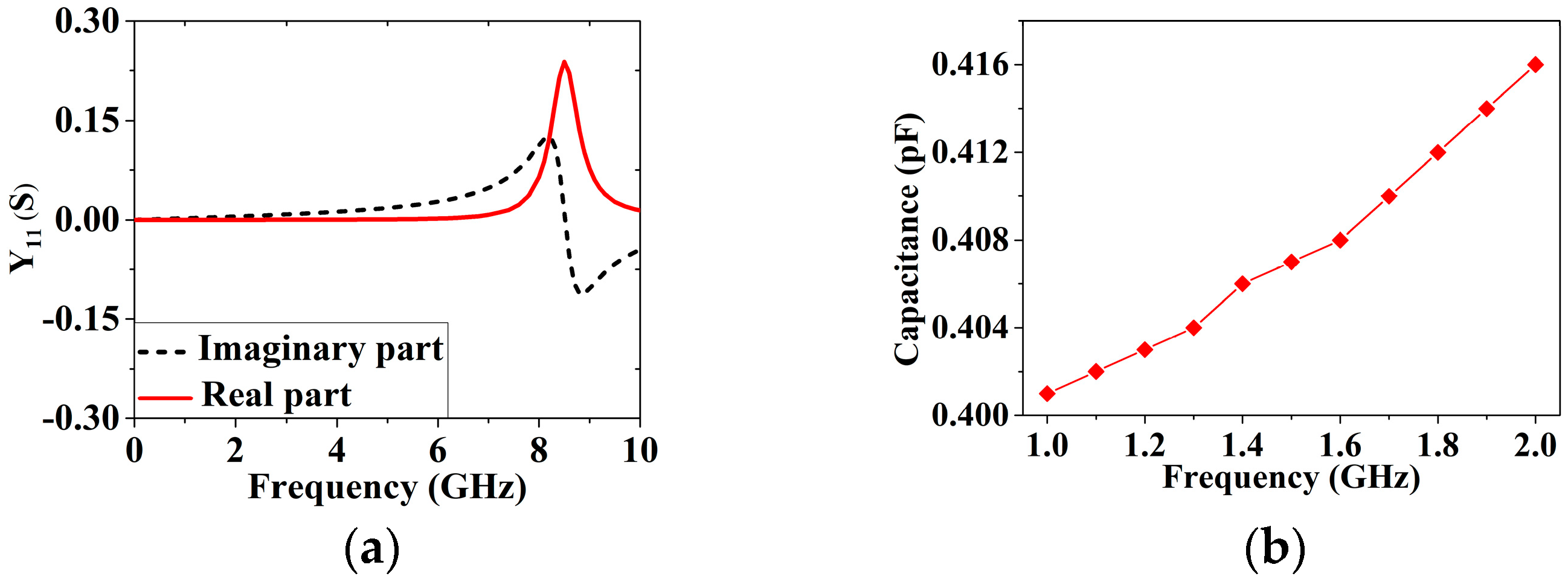
The simulations and optimization were performed on the Agilent Advanced Design System Momentum version 2016.01 (Keysight Technologies, Inc., Santa Rosa, CA, USA) to confirm and support the results and theoretical analysis in this study. The simulated Y parameter of the inner spiral line is depicted in Figure 2a. From this curve, a value of 0.405 pF at a resonant frequency of 1.35 GHz was calculated as in [18]:
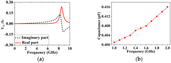
Figure 2.
Simulation results of capacitance for optimization. (a) Y parameter of the inner spiral line; (b) Calculated capacitance value.
As shown in Figure 2b, in the L band, where most of the satellite communication systems operate, the capacitance value is stable as only minor differences can be observed. The inductor and capacitor are connected in series, and the center frequency related to the total inductance and capacitance can be expressed as in [18]:
the error between the calculated and designed resonant frequencies does not exceed 2.3%.
A representative cross-section of the technology used for the proposed design is illustrated in Figure 3a, where the dimensions are not to scale. The structure is mainly composed of a GaAs substrate and metal layers. Only three metal surfaces, which are the Leads layer, Text layer, and Bond layer from top to bottom, are presented to make the design and processing more concise. The relatively inexpensive copper/gold metal is preferred for slowing down oxidation. The seed metal is selectively added to increase adhesion. A thin SiNx layer is deposited on the 200 μm thick GaAs substrate, to form a flat surface, and top metal for long-term protection, with a thickness of 100 nm [19,20,21]. The dielectric constant (εr) of GaAs is 12.85, with a loss tangent of 0.006. The finest line width can be processed to 10 μm, with a thickness of 1.8 μm as a middle metal layer. Small gaps between the two metal layers can be used to build an air bridge. More details on the processing are detailed in Figure 3b. After cleaning, plasma-enhanced chemical vapor deposition is used to deposit the SiNx layer on the substrate. The thickness of Cu/Au is 4.5/0.5 μm, as the bottom metal and the top metal. A plasma etcher (SF6:O2 = 45:5 sccm) is adopted after depositing a dielectric layer to remove the unnecessary parts of SiNx. A 100 nm thick Ti/Au seed metal deposition is followed by etching to avoid shorting, and another mask can be selectively used on the protective film of the top metal to form the specific area of the final SiNx layer.
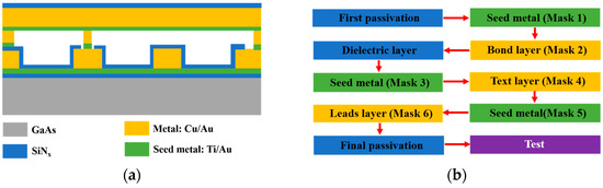
Figure 3.
Employed advanced integrated passive device (IPD) technology. (a) Stack-up of device on GaAs substrate; (b) Flowchart of the IPD fabrication process.
3. Results
For testing, the signal from the chip was directed outside through the gold leads on both sides, as shown in Figure 4a, and the chip was attached to a sub-board, as shown in Figure 4b. Figure 4c shows a cubic aluminum block with edges of 2 cm, placed on the bottom of the printed circuit board. The aluminum block provides a flat measuring environment and noise reduction. Figure 4d shows the Agilent 8719ES vector network analyzer that was used to perform measurements on the fabricated BPF.
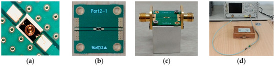
Figure 4.
Measurement setup. (a) Enlarged view of on-chip BPF with Au wire bonding; (b) Packaged device on a printed circuit board; (c) Side view of the final product with connectors; (d) Test setup.
The total size of the proposed BPF is 1.54 mm × 0.81 mm, which corresponds to a size of (2.4 × 10−2 × 1.3 × 10−2)∙λg, where λg denotes the guided wavelength at a center frequency of 1.35 GHz. Figure 5a shows the scanning electron microscopy image that is used to verify whether the processing is defective or not, as this would be difficult to observe with the naked eye. The simulated current density around the resonant frequency is shown in Figure 5b, which indicates the current flowing through the center of the filter, and reflects the internal workings of the central region of the filter at resonance. The Q-factor represents the amount of energy that is lost on the filter, with higher values indicating greater loss. The Q-factor of the BPF can be calculated as:
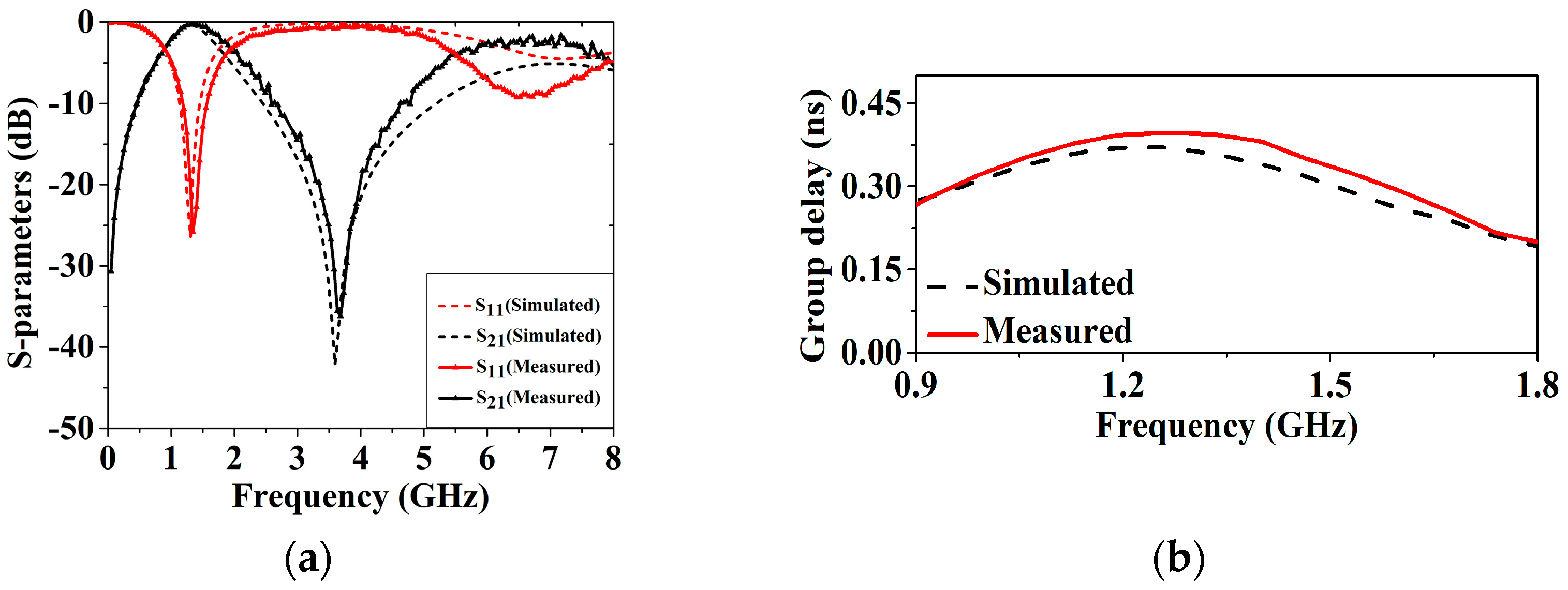
where fH and fL are passband-edge frequencies in the upper and lower bands, respectively. As shown in Figure 6a, a 10 dB fractional impedance bandwidth of 29% was achieved, the fractional bandwidth is calculated by (fH − fL)/fc [18]. The insertion loss is as low as 0.26 dB, and the return loss is above 25.6 dB within the passband. A transmission zero is designed to locate at 3.7 GHz, where the admittance parameter Y21 equals zero, with a magnitude of S21 to be 36 dB in the rejection band. The location of transmission zero can be slightly changed with the dimension; however, it should be noted that it may affect the variations of other parameters, such as bandwidth and selectivity [18,21]. A sharp roll-off is obtained both in the lower and upper bands, from 20 dB to 3 dB attenuation points, which confirms the good skirt performance. A relatively constant group delay over the entire passband is plotted in Figure 6b, indicating the small distortion of the BPF. The negligible differences between the measurement and simulation results may be due to losses in the measuring instruments.
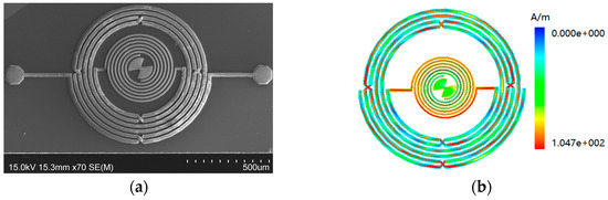
Figure 5.
Final processed on-chip BPF. (a) Scanning electron microscopy image of proposed BPF; (b) Simulated current density over proposed BPF.
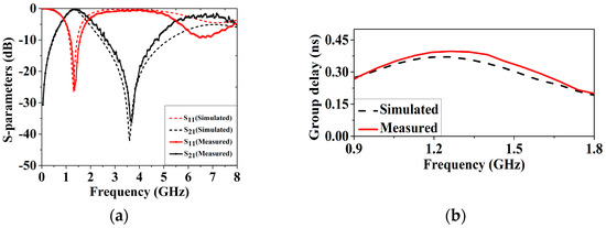
Figure 6.
Simulation and measurement results: (a) Parameters S11 and S21; (b) Group delay.
4. Discussion
Research on BPFs mainly aims for their application to wired and wireless communication systems. In addition, IPD technology is used to meet the high demands of modern communication equipment regarding micromachining. Moreover, GaAs, a high mobility material, is usually applied as a substrate because its process is more mature than most other processes, and there is no excess passivation film on the GaAs surface. Long transmission lines designed in the pattern improve processing precision, which further ensures the stability of the filter. In this study, a simple inductor–capacitor series equivalent circuit is used for analysis. Problems can be found in time in low-order circuit and be modified easily. Then, after repeated simulations and measurements, loss was reduced and a wide bandwidth was achieved. Finally, fabricated BPF was checked to confirm that there is no problem through the scanning electron microscopy images.
Many studies have been focused on improving the performance of BPFs in recent years. Table 1 compares on-chip filters based on different processes with the proposed BPF, which provides higher performance with fewer metal layers than a low temperature co-fired ceramic BPF [8] or a glass IPD BPF [22]. The return loss above 20 dB of the proposed BPF indicates that almost no reflected signal occurs at the center frequency, and the best insertion loss was obtained among the compared BPFs [8,21,22,23,24,25]. GaAs can provide better insulation and less signal loss than silicon substrate; in addition, the working power of GaAs is higher than glass [26]. A circular spiral pattern is used in series with the inductor, and the stability of the capacitance value is ensured by the simple structure in a limited space. A relatively high self-resonant frequency of the capacitor, which is approximately equal to 8.1 GHz, enables the capacitor to work over a wide frequency range. The overall size of fabricated chip is small, especially the circular structure that makes the short side more compact.

Table 1.
Comparison of this study to similar works.
5. Conclusions
We propose a simple design of an IPD-based BPF for L-band applications. A circular spiral inductor with an embedded capacitor is used to reduce the chip size to 1.25 mm2. High performance in terms of return loss and insertion loss with values of 25.6 dB and 0.26 dB, respectively, were measured throughout the passband. The theoretically predicted values are in good agreement with the actual measured values. By fabrication on a GaAs substrate, it is possible to perform a relatively high Q-factor and a compact spiral circular pattern. Additionally, fabrication costs and time can be saved with this simple IPD processing technology, by using three layers of metal. IPDs can effectively combine plenty of passive components together to save more space and achieve more features than discrete passive devices.
IPD technology whose substrate possesses good insulation properties and high electron mobility in a high frequency range will have broad application prospects in medical, lighting, and wireless communication markets. In our future work, the chip will be packaged to prevent damage and overheating by adopting a SOT-6 packaging process, which also provides waterproofing and easy handling. Considering these advantages along with its high selectivity, the proposed BPF seems promising for applications in wireless communication systems.
Author Contributions
Conceptualization, C.-H.Q.; Methodology, C.-H.Q.; Software, Z.-J.W.; Validation, J.-C.L.; Formal analysis, C.-H.Q.; Investigation, C.-H.Q.; Resources, E.-S.K.; Data curation, Z.-J.W.; Writing—original draft, C.-H.Q.; Writing—review and editing, J.-C.L. and N.-Y.K.; Visualization, Z.-J.W.; Supervision, N.-Y.K.
Funding
This work was supported by the National Research Foundation of Korea (NRF) grant funded by the Korea government (Ministry of Science and ICT) (No.2016R1D1A1B03935640).
Conflicts of Interest
The authors declare no conflict of interest.
References
- Huang, C.H.; Chen, C.H.; Horng, T.S. Compact Bandpass Filter Using Novel Transformer-Based Coupled Resonators on Integrated Passive Device Glass Substrate. Microw. Opt. Technol. Lett. 2012, 54, 3–7. [Google Scholar] [CrossRef]
- Lalbakhsh, A.; Karimi, G.; Sabaghi, F. Triple Mode Spiral Wideband Bandpass Filter Using Symmetric Dual-Line Coupling. Electron. Lett. 2017, 53, 795–797. [Google Scholar] [CrossRef]
- Huang, F.; Wang, J.; Li, J.; Wu, W. Compact Microstrip Wideband Bandpass Filter with High Selectivity. Electron. Lett. 2016, 52, 626–628. [Google Scholar] [CrossRef]
- Gao, L.; Zhang, X.Y.; Hu, B.J.; Xue, Q. Novel Multi-Stub Loaded Resonators and Their Applications to Various Bandpass Filters. IEEE Trans. Microw. Theory Tech. 2014, 62, 1162–1172. [Google Scholar] [CrossRef]
- Lan, S.W.; Weng, M.H.; Chang, S.J.; Hung, C.Y.; Liu, S.K. A Tri-Band Bandpass Filter with Wide Stopband Using Asymmetric Stub-Loaded Resonators. IEEE Microw. Wirel. Compon. Lett. 2015, 25, 19–21. [Google Scholar] [CrossRef]
- Xu, J.; Zhu, Y. Compact Semi-Lumped Dual- and Tri-Wideband Bandpass Filters. IET Microw. Antennas Propag. 2017, 11, 53–58. [Google Scholar] [CrossRef]
- Mukherjee, S.; Mutnury, B.; Dalmia, S.; Swaminathan, M. Layout-Level Synthesis of RF Inductors and Filters in LCP Substrates for Wi-Fi Applications. IEEE Trans. Microw. Theory Tech. 2005, 53, 2196–2210. [Google Scholar] [CrossRef]
- Arabi, E.; Lahti, M.; Vähä-Heikkilä, T.; Shamim, A. A 3-D Miniaturized High Selectivity Bandpass Filter in LTCC Technology. IEEE Microw. Wirel. Compon. Lett. 2014, 24, 8–10. [Google Scholar] [CrossRef]
- Yang, Y.; Liu, H.; Hou, Z.J.; Zhu, X.; Dutkiewicz, E.; Xue, Q. Compact On-Chip Bandpass Filter with Improved In-Band Flatness and Stopband Attenuation in 0.13-μm (Bi)-CMOS Technology. IEEE Electron. Device Lett. 2017, 38, 1359–1362. [Google Scholar] [CrossRef]
- Adhikari, K.K.; Kim, N.Y. Ultrahigh-Sensitivity Mediator-Free Biosensor Based on a Microfabricated Microwave Resonator for the Detection of Micromolar Glucose Concentrations. IEEE Trans. Microw. Theory Tech. 2016, 64, 319–327. [Google Scholar] [CrossRef]
- Qiang, T.; Wang, C.; Kim, N.Y. A Compact High-Reliability High-Performance 900-MHz WPD Using GaAs-IPD Technology. IEEE Microw. Wirel. Compon. Lett. 2016, 26, 498–500. [Google Scholar] [CrossRef]
- Jung, J.W.; Nae, K.K.; Kim, J.; Park, J.S. RF-IPD Directional Coupler for Mobile RFID Handset Applications. Electron. Lett. 2007, 53, 719–720. [Google Scholar] [CrossRef]
- Aryan, N.P. Design and Modeling of Inductors, Capacitors and Coplanar Waveguide at Tens of GHz Frequencies, 1st ed.; Springer: New York, NY, USA, 2014; pp. 19–34. ISBN 978-3-319-10187-3. [Google Scholar]
- Haobijam, G.; Palathinkal, R.P. Design and Analysis of Spiral Inductors, 1st ed.; Springer: New York, NY, USA, 2013; pp. 37–38. ISBN 978-81-322-1514-1. [Google Scholar]
- Mohan, S.S.; del Mar Hershenson, M.; Boyd, S.P.; Lee, T.H. Simple Accurate Expressions for Planar Spiral Inductances. IEEE J. Solid-State Circuits 1999, 34, 1419–1424. [Google Scholar] [CrossRef]
- Chen, T.; Bowler, N. Design of Interdigital Spiral and Concentric Capacitive Sensors for Materials Evaluation. AIP Conf. Proc. 2013, 1511, 1593–1600. [Google Scholar] [CrossRef]
- Chen, T.; Bowler, N. Analysis of a Concentric Coplanar Capacitive Sensor for Nondestructive Evaluation of Multi-Layered Dielectric Structures. IEEE Trans. Dielectr. Electr. Insul. 2010, 17, 1307–1318. [Google Scholar] [CrossRef]
- Hong, J.S. Microstrip Filters for RF/Microwave Applications, 2nd ed.; John Wiley & Sons: Hoboken, NJ, USA, 2011; pp. 203–263. ISBN 978-0-470-40877-3. [Google Scholar]
- Qiang, T.; Wang, C.; Kim, N.Y. High-Performance and High-Reliability SOT-6 Packaged Diplexer Based on Advanced IPD Fabrication Techniques. Solid-State Electron. 2017, 134, 9–18. [Google Scholar] [CrossRef]
- Lai, C.H.; Zhou, G.T.; Ma, T.G. On-Chip Miniaturized Diplexer Using Jointed Dual-Mode Right-/Left-Handed Synthesized Coplanar Waveguides on GIPD Process. IEEE Microw. Wirel. Compon. Lett. 2014, 24, 245–247. [Google Scholar] [CrossRef]
- Wang, Z.J.; Kim, E.S.; Liang, J.G.; Qiang, T.; Kim, N.Y. A High-Frequency-Compatible Miniaturized Bandpass Filter with Air-Bridge Structures Using GaAs-Based Integrated Passive Device Technology. Micromachines 2018, 9, 463. [Google Scholar] [CrossRef] [PubMed]
- Sitaraman, S.; Sukumaran, V.; Pulugurtha, M.R.; Wu, Z.; Suzuki, Y.; Kim, Y.; Sundaram, V.; Kim, J.; Tummala, R.R. Miniaturized Bandpass Filters as Ultrathin 3-D IPDs and Embedded Thinfilms in 3-D Glass Modules. IEEE Trans. Compon. Packag. Manuf. Technol. 2017, 7, 1410–1418. [Google Scholar] [CrossRef]
- Wong, K.W.; Mansour, R.R.; Weale, G. Reconfigurable Bandstop and Bandpass Filters with Wideband Balun Using IPD Technology for Frequency Agile Applications. IEEE Trans. Compon. Packag. Manuf. Technol. 2017, 7, 610–620. [Google Scholar] [CrossRef]
- Chuluunbaatar, Z.; Adhikari, K.K.; Wang, C.; Kim, N.Y. Micro-Fabricated Bandpass Filter Using Intertwined Spiral Inductor and Interdigital Capacitor. Electron. Lett. 2014, 50, 1296–1297. [Google Scholar] [CrossRef]
- Lee, K.H.; Kim, E.S.; Liang, J.G.; Kim, N.Y. Design and Realization of a Compact High-Frequency Band-Pass Filter with Low Insertion Loss Based on a Combination of a Circular-Shaped Spiral Inductor, Spiral Capacitor and Interdigital Capacitor. Electronics 2018, 7, 195. [Google Scholar] [CrossRef]
- Kim, N.Y.; Wang, C.; Li, Y. Introduction to Integrated Passive Device Technology, 1st ed.; LAP LAMBERT Academic Publishing: Riga, Latvia, 2016; p. 44. ISBN 978-3-659-82363-3. [Google Scholar]


© 2019 by the authors. Licensee MDPI, Basel, Switzerland. This article is an open access article distributed under the terms and conditions of the Creative Commons Attribution (CC BY) license (http://creativecommons.org/licenses/by/4.0/).