Article

Neoteric Fuzzy Control Stratagem and Design of Chopper fed Multilevel Inverter for Enhanced Voltage Output Involving Plug-In Electric Vehicle (PEV) Applications

by
Suvetha Poyyamani Sunddararaj
1,*,
Shriram S. Rangarajan
2,*,† and
Swaminathan Gopalan
1
1
Department of Electrical and Electronics Engineering, SASTRA Deemed University, Tamil Nadu 613401, India
2
Department of Electrical and Computer Engineering, Clemson University, Clemson, SC 29634, USA
*
Authors to whom correspondence should be addressed.
Current Affiliation: Department of Electrical and Electronics Engineering, SASTRA Deemed University, Tamil Nadu 613404, India.
Electronics 2019, 8(10), 1092; https://doi.org/10.3390/electronics8101092
Submission received: 31 August 2019 / Revised: 24 September 2019 / Accepted: 25 September 2019 / Published: 26 September 2019
(This article belongs to the Section Power Electronics)

Abstract

:
The utilization of plug-in electric vehicles (PEV) has started to garner more attention worldwide considering the environmental and economic benefits. This has led to the invention of new technologies and motifs associated with batteries, bidirectional converters and inverters for Electric Vehicle applications. In this paper, a novel design and control of chopper circuit is proposed and configured with the series and parallel connection of the power electronic based switches for two-way operation of the converter. The bidirectional action of the proposed converter makes it suitable for plug-in electric vehicle applications as the grid is becoming smarter. The DC–DC converter is further interfaced with the designed multilevel inverter (MLI). The reduced switches associated with the novel design of MLI have overcome the cons associated with the conventional inverters in terms of enhanced performance in the proposed design. Further, novel control strategies have been proposed for the DC–DC converter based on Proportional Integral (PI) and Fuzzy based control logic. For the first time, the performance of the entire system is evaluated based on the comparison of proposed PI, fuzzy, and hybrid controllers. New rules have been formulated for the Fuzzy based controllers that are associated with the Converter design. This has further facilitated the interface of bidirectional DC–DC converter with the proposed MLI for an enhanced output voltage. The results indicate that the proposed hybrid controller provides better performance in terms of voltage gain, ripple, efficiency and overall aspects of power quality that forms the crux for PEV applications. The novelty of the design and control of the overall topology has been manifested based on simulation using MATLAB/SIMULINK.

1. Introduction

Plug-in electric vehicles (PEV)-based technology has gained a lot of interest considering the environmental concerns to reduce pollutant emissions and its contribution towards green energy. The recent development in the concepts of smart grid and microgrid, smart meters, and smart homes anticipates PEVs to emerge as a smart solution for transportation [1,2,3,4,5].
It could be seen from Figure 1 that the Smart Grid comprises of several domains. One such domain of IEEE 2030 Interoperability Standard is the effective interaction of renewable energy resources and PEVs with the power system network [6]. The electric vehicle systems are mainly battery-based and plug-in topologies. Usually, a battery is incorporated for absorbing the regenerative breaking and to achieve good transient performance. In order to interface the PEV’s with the grid, converters and inverters are required. The performance of EV’s are enhanced in terms of power quality and efficiency when they are fed with a controlled high gain converter topologies. The high gain (step-up) and isolation between source and load segments in DC–DC converters can be easily achieved by using high frequency isolated topologies. But the drawbacks associated with these kinds of topologies are numerous. To overcome the limitations, non-isolated converters are implemented [7]. These types of converters utilize mutually coupled inductors instead of heavy and highly rated transformers which lead to losses. The coupled inductor configurations have less input current ripple and possess better internal characteristics. Apart from this, many research works are being carried out involving DC–DC converters, such as bidirectional circuits, dual active bridge, and voltage-doubler cell that provide better output performance [8,9,10]. The controlled converters are more beneficial in terms of gain, ripple and fast operations. Papers in literature have implemented converters based on conventional controllers like PID [11,12]. Multilevel inverter (MLI) topologies have gained more attention due to its advantages such as high efficiency, reduced harmonics (enhanced power quality), and better electromagnetic interference (EMI). MLIs are classified into many types based on the connection and devices used in the configuration [13].
In this paper, there are several contributions in the form of research. Several new controllers based on PI and Fuzzy controllers are proposed for the DC–DC converter. Further, a hybrid controller has also been proposed for the DC–DC converter. The DC–DC converter is further fed to a newly developed MLI with a single voltage source and reduced power electronic switches. The enhanced performance in terms of power quality and output voltage from the proposed design and controllers forms the quintessence of PEV applications before being interfaced with the grid. So far, none of the research work in literature have discussed about developing new controllers for PEV applications towards enhanced performance of the converter output. The enhanced performance in the output voltage plays a vital role in the synchronization of PEVs with the smart grid. For the first time, the performance comparison of the entire converter system with the novel proposed PI, fuzzy and hybrid controllers are manifested in this paper. New rules have been devised for the Fuzzy based controllers. Research outcome of this paper in the form of simulation using MATLAB/SIMULINK clearly depicts that the proposed novel controllers for novel converter design provides better performance in terms of voltage gain, ripple, efficiency and overall aspects of power quality.

2. Chopper Configuration

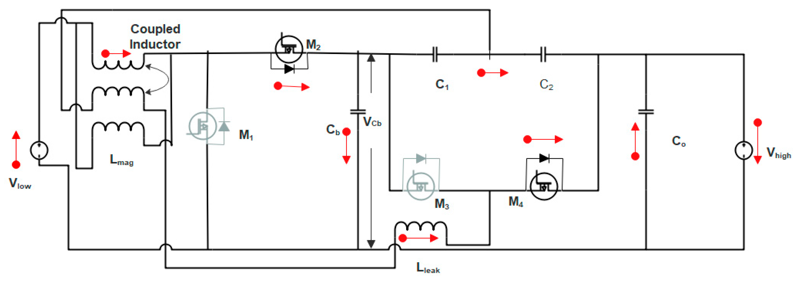
The circuit topology of the proposed converter comprises of a DC source input voltage Vs, the power MOSFET switches M1-M4, capacitors Cb, C1, and C2, and the coupled inductor with primary and secondary winding, Np and Ns respectively. The model of the coupled inductor bidirectional DC–DC converter also has a magnetizing inductor Lmag and a leakage inductor Lleak. The coupled inductor configuration provides high voltage gain and the reduced current ripple. The high conversion gain (boost mode) can be achieved by voltage doubler cell mechanism [14] based on the capacitor Cb. The proposed chopper circuit is shown in Figure 2.
The voltage conversion is improved by inserting the secondary winding of coupled inductor into the voltage doubler cell. The primary winding along with the magnetizing inductor i.e, Lmag acts as a filter for the converter. The switches M1, M2, M3, and M4 are connected in series and form a switch bridge between the high voltage side Vh and battery voltage Vb. The two bridges are divided by a common capacitor Cb. The segment of Vh and Cb is the conventional buck-boost bidirectional converter and the latter is a dual active half bridge (DAHB) bidirectional converter. Due to the minimization of circulating current and soft switching mechanism of switches, highest efficiency can be perceived. The voltage matching can be made easily with this proposed configuration. Since the output voltage of Vcb is fed to the input terminal of DAHB bidirectional converter (BDC), the voltage control on the two windings of coupled inductor is achieved. It can be mathematically denoted as follows:
V c b ( V h V c b ) =   N 1 N 2 =   1 n
The significance of the converter circuit used in this work is listed below:
  • Since, the voltage on the two segments of the converter are matched with that of the turns ratio of coupled inductor, the current circulating across the switches are reduced and soft switching is also accomplished.
  • High voltage conversion is achieved with the transformer less configuration.
  • High power density is attained due to the winding of inductors on the same core.

2.1. Operating Modes

The proposed bidirectional DC–DC converter has two operating modes, i.e., step-down mode and step-up mode based on whether the PEV is charging or discharging respectively. The switching states are as follows.

2.1.1. Mode I (t0 < t < t1)

Due to the negative currents ib and iLleak the switch M2 and M4 is turned ON. The switch M2 gets turned off at t0 and the parasitic diode of M1 is ON due to the negative current of ib. The equivalent circuit for mode I is shown in Figure 3.

2.1.2. Mode II (t1 < t < t2)

During mode 1 [t0, t1] and mode 2 [t1, t2], the magnetizing and leakage currents increases linearly due to the positive voltage on the corresponding inductors. The equivalent circuit for mode II is shown in Figure 4.

2.1.3. Mode III (t2 < t < t3)

In this mode, M4 is turned off at t2, the parasitic diode of M3 is ON due to the positive value of leakage current. The equivalent circuit for mode III is shown in Figure 5.

2.1.4. Mode IV (t3 < t < t4)

During mode 3 [t2, t3] and mode 4 [t3, t4], the battery is discharged and supplies power to the load. So, the magnetizing inductor is charged by Vb, and iLmag keeps increasing linearly. In this stage the battery power is supplied to the high voltage side, and Cb is charged while Co is discharged. The equivalent circuit for mode IV is shown in Figure 6.

2.1.5. Mode V (t4 < t < t5)

In this mode M1 is turned off at t4, and the parasitic diode of M2 is ON due to the positive values of magnetizing and leakage currents. The equivalent circuit for mode VII is shown in Figure 7.

2.1.6. Mode VI (t5 < t < t6)

During mode 5 [t4, t5] and mode 6 [t5, t6], both magnetizing and leakage currents decreases linearly. Both the battery and the energy stored in Lmag are discharged and supply power to the capacitor C1. The equivalent circuit for mode VI is shown in Figure 8.

2.1.7. Mode VII (t6 < t < t7)

At t6, M3 is turned off and the parasitic diode of M4 conducts because of the negative value of leakage current. The equivalent circuit for mode VII is shown in Figure 9.

2.1.8. Mode VIII (t7 < t < t8)

In mode 7 [t6, t7] and mode 8 [t7, t8], the battery is discharged and supply power to the high-voltage side, and C2 is discharged while Co is charged. The equivalent circuit for mode VIII is shown in Figure 10.

2.2. Voltage Equations

2.2.1. Voltage Conversion Ratio

The Voltage conversion ratio is given by the following equation,
G   =   Vh Vb =   ( n + 1 ) ( 1 D )
where,
G—Voltage gain
Vh—High voltage
Vb—Battery voltage
n—Turns ratio
D—Duty ratio

2.2.2. Voltage across Capacitance

The voltage across various capacitances is,
Vc b =   V b ( 1 D )
Vc 1 =   ( 1 D ) ( V h V c b ) = n V b
Vc 2 = D ( V h V c b ) = D ( 1 D ) n V b
where,
Vcb—Voltage across capacitor Cb
Vc1—Voltage across capacitor C1
Vc2—Voltage across capacitor C2
D—Duty ratio
n—Turns ratio

3. Multilevel Inverter

The proposed nine level inverter consists of two circuits, one is a developed SC circuit (DSCC) at the frontend of the inverter and another circuit is a conventional H-bridge circuit. The H-bridge circuit connected at the backend of the inverter is used for producing the negative voltage levels of the output [15,16,17]. The circuit configuration of multilevel inverter is shown in Figure 11.
The hybrid multilevel inverter can be operated based on the following switching sequence and it can produce nine level output. The switching sequences are given in Table 1.
  • To acquire the voltage level of +2Vdc the switches S1, S4 of the H-bridge circuit and the switches S5, S6, and S7 of the DSCC circuit is held High.
  • To acquire the voltage level of +3Vdc/2 the switches S1, S4 of the H-bridge circuit and the switches S5, S6, and S9 of the DSCC circuit is held High.
  • The voltage level of +Vdc is achieved by holding the switches S1 and S4 of the H-bridge circuit and the switches S5 and S8 of the DSCC circuit at High position.
  • To obtain the next level of multilevel output i.e., +Vdc/2, the switches S1 and S4 of the H-bridge circuit and the switches S8 and S9 of the DSCC circuit is held High.
  • The zero level voltage is obtained by holding the switches S2 and S4 of the H-bridge circuit and the switches S8 and S9 of the DSCC circuit at High position.
  • To achieve the voltage level of –Vdc/2, the switches S2 and S3 of the H-bridge circuit and the switches S8 and S9 of the DSCC circuit is held High.
  • The negative cycle of Vdc (i.e., –Vdc) is achieved by holding the switches S2 and S3 of the H-bridge circuit and the switches S5 and S8 of the DSCC circuit is held High.
  • To obtain the voltage level of –3Vdc/2, the switches S2 and S3 of the H-bridge circuit and the switches S5, S6, and S9 of the DSCC circuit is held High.
  • To acquire the voltage level of –2Vdc the switches S2 and S3 of the H-bridge circuit and the switches S5, S6, and S7 of the DSCC circuit is held High.

4. Controller Circuit

4.1. PI Controller

The PI controller is one of the familiar techniques used for controlling a system. It is mainly used to eliminate the steady state error. This type of controller produces an output signal containing two terms, one proportional to the operating signal and the other proportional to its integral [18]. The block diagram of the proposed system with PI controller for both voltage and current control is shown in Figure 12.
The closed loop system shown in above Figure 12, regulates the voltage and current by comparing the actual value with the desired value. In this system, the high voltage (Vh) is compared with a reference voltage and an error is generated. This error signal is given to the controller block where the control process is carried out and a steady state value is generated. Similarly, the control of current block is carried out. Some of the drawbacks of this system are high rise time and settling time, less speed of the response. To overcome this, fuzzy logic control is introduced because of its simplicity, ease of design and ease of implementation. The above mentioned drawbacks are comparatively less in a fuzzy based system. The designed values for PI controller is given in Table 2.

4.2. Proposed Fuzzy Logic Based Controller

Fuzzy logic control (FLC) is a technique to epitomize human-like thinking into a control system. It works based on the concept of human deductive thinking to infer conclusions from the past experience and is designed to emulate the former. The typical control system is usually modeled with a physical reality whereas the fuzzy controller incorporates equivocal human logic into programs [19,20,21,22]. This fuzzy logic is applicable for systems which is difficult to represent by mathematical models. The basic block diagram of fuzzy logic controller is shown in Figure 13.

4.2.1. Rule 1

In the first rule, two input variables such as ‘error (e)’ and ‘change in error (ce)’ are taken along with an output variable ‘Output1’. Triangular membership function is used for all the variables in the given fuzzy set. For input 1 and input 2 (i.e.) error and change in error, the linguistic variables Negative (N), Zero (Z), and Positive (P) are assumed. For output, the variables are taken as Low (L), Medium (M) and High (H). The proposed rule is given in Table 3.
The input and output membership functions for the above-mentioned rule is given below in Figure 14 a–c respectively.
The overall rule viewer is shown in Figure 15.
The surface view of rule 1 is shown in Figure 16.
Figure 16, shows the 3D view of the proposed fuzzy rule. In this plot, the error and change in error are taken along the x and y-axis whereas the output is taken along the z-axis.

4.2.2. Rule 2

In this rule, two input variables such as ‘error (e)’ and ‘change in error (ce)’ are taken along with an output variable ‘Output1’. In this case, combinations of two different membership functions are used i.e., Trapezoidal MF for Input 1 and Gauss MF for Input 2. The output membership function is given by Triangular MF. For input 1 and input 2 (i.e.) error and change in error, the linguistic variables Negative Big (NB), Negative Small (NS), Zero (Z), Positive Small (PS), and Positive Big (PB) are assumed. For output, the variables are taken as Very Large (VL), Large (L), Medium (M), High (H), and Very High (VH). The proposed rule is given in Table 4.
The input and output membership functions for the above-mentioned rule is given below in Figure 17.
The overall rule viewer is shown in Figure 18.
The surface view of rule 2 is shown in Figure 19.
Figure 19, shows the 3D view of the proposed fuzzy rule. In this plot, the error and change in error are taken along the x and y-axis whereas the output is taken along the z-axis.

4.2.3. Rule 3

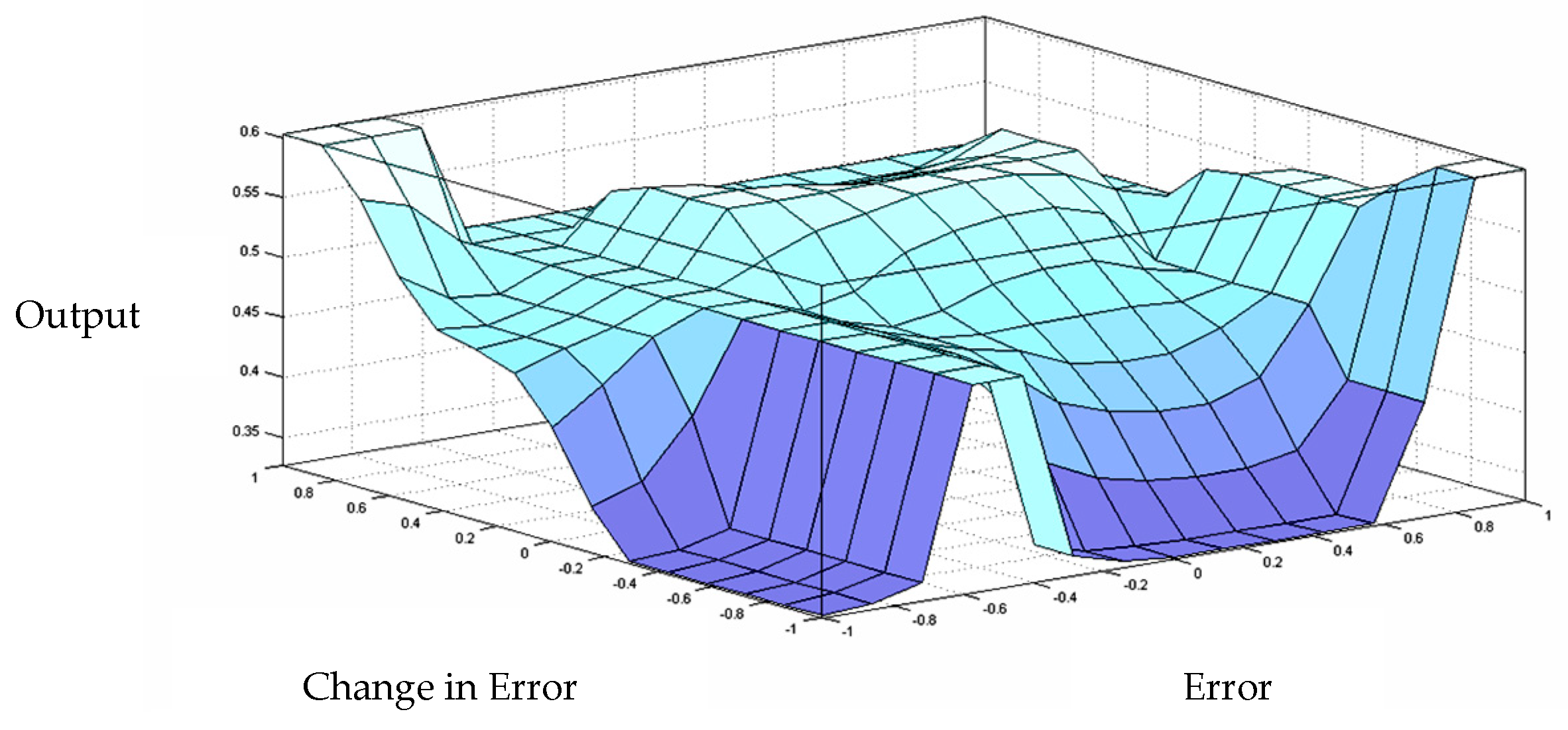
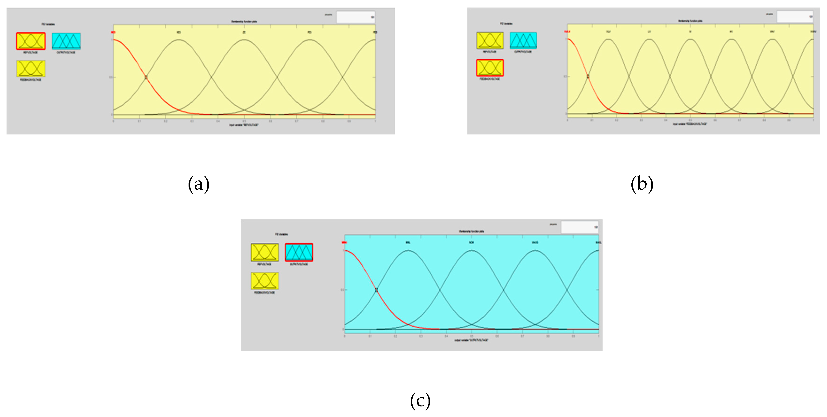
In this rule, two input variables such as ‘error (e) (Reference Voltage) ’ and ‘change in error (ce) (Feedback Voltage)’ are taken along with an output variable ‘Output1’. Here Gauss MF is used for all the three cases. For input 1 and input 2 (i.e.) error and change in error, the linguistic variables Negative Error Big (NE-B), Negative Error Small (NE-S), Zero Error (ZE), Positive Error Small (PE-S) and Positive Error Big (PE-B) are assumed. For output, the variables are taken as Very Very Low Voltage (VVLV), Very Low Voltage (VLV), Low Voltage (LV), Medium (M), High Voltage (HV), Very High Voltage (VHV) and Very Very High Voltage (VVHV). The proposed rule is given in Table 5.
The input and output membership functions for the above-mentioned rule is given below in Figure 20.
The overall rule viewer is shown in Figure 21.
The surface view of rule 3 is given in Figure 22.
Figure 22, shows the 3D view of the proposed fuzzy rule. In this plot, the error (reference voltage) and change in error (feedback voltage) are taken along the x-axis and y-axis whereas the output voltage is taken along the z-axis.

4.2.4. Rule 4

In this rule, two input variables such as ‘error (e) (Reference Current)’ and ‘change in error (ce) (Feedback Current)’ are taken along with an output variable ‘Output1’. In this case, combinations of two different membership functions are used i.e., Trapezoidal MF for Input 1 and Gauss MF for Input 2. The output membership function is given by g-bell MF. For input 1 and input 2 (i.e) error and change in error, the linguistic variables such as −2.5, −1.5, 0, 1.5, 2.5 are assumed. For output, the variables are taken as −1.01, −0.31, −0.01, 0.29, 0.99. The proposed rule is given in Table 6.
The input and output membership functions for the above mentioned rule is given below in Figure 23.
The overall rule viewer plot is shown in Figure 24.
The surface plot for rule 4 is given in Figure 25.
Figure 25 shows the 3D view of the proposed fuzzy rule. In this plot, the error (reference current) and change in error (feedback current) are taken along the x and y-axis whereas the output is taken along the z-axis.
The schematic of proposed fuzzy logic controller is shown in Figure 26.
Individual controllers for voltage and current are designed using fuzzy technique. The reference value is compared with the feedback value and an error is generated. This error is fed to the fuzzy inference engine along with the change in error value for fuzzification process. Finally, the fuzzified value is generated and is converted to crisp set by defuzzification process before feeding it to the converter system.

4.3. Novel Hybrid Controller

The hybrid controller is the combination of PI and Fuzzy Logic Controller. In this paper, the four different configurations of hybrid controllers are proposed:

4.3.1. Proposed Hybrid Controller-1

In this configuration, the voltage control of the converter is done with a hybrid controller made up of Fuzzy and PI controller. The block diagram of hybrid controller-1 is shown in Figure 27.
The reference voltage is compared with a feedback voltage and an error signal is generated. The generated error signal and change in error signal is fed to the fuzzy controller. Both the signals are fuzzified based on the proposed rule base and the defuzzified output is given to the PI controller. The signal generated by the PI controller is given to the MOSFET switches.
The current control is done using a PI controller and the diagram is shown in Figure 28.

4.3.2. Proposed Hybrid Controller-2

In hybrid controller-2, Individual Fuzzy controllers are used for error and change in error signals. The fuzzifiedoutput is converted into a crisp value by taking a product of the output signal and the error. The same process is carried out for the change in error signal and both the signals are compared and fed to a PI controller for further accuracy. The block diagram for voltage control is shown in Figure 29.
The current is controlled with the help of a PI controller. The control process is depicted in below Figure 30.

4.3.3. Proposed Hybrid Controller-3

The third configuration of hybrid controller implements fuzzy logic for both the voltage and current control. The block diagram of both the voltage and current control is shown in Figure 31, respectively.
Figure 32 shows the control block for the current using fuzzy logic technique.

4.3.4. Proposed Hybrid Controller-4

This configuration is similar to that of type-2 hybrid controller. In voltage control, the fuzzified output of both error and change in error signals are converted into a crisp value by taking a product of the output signal and the input error signals. These signals are compared and fed to a PI controller for further accuracy. Here, the current is also controlled by fuzzy based system. The block diagram for each control technique is shown in Figure 33 and Figure 34 respectively.

5. Simulation Result

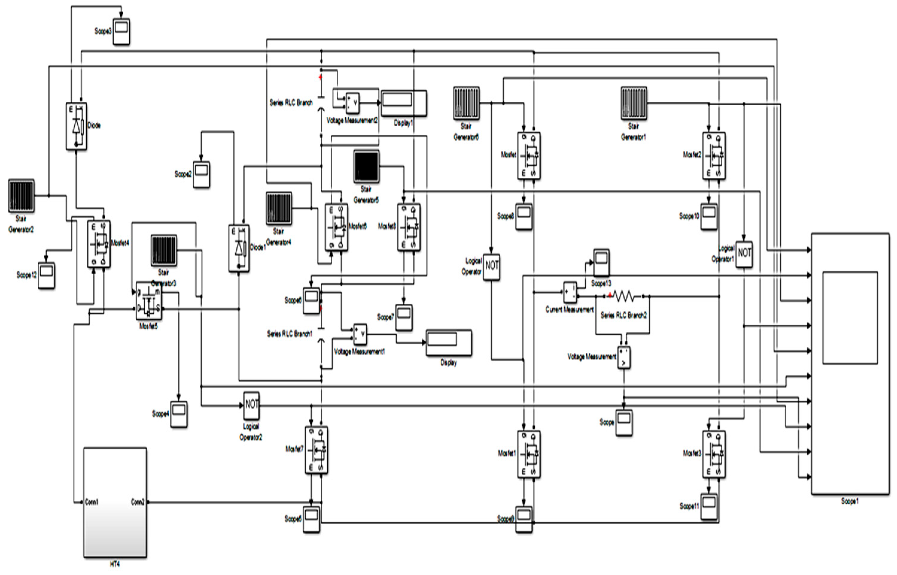
The proposed chopper and inverter circuit is tested with different proposed controllers based on PI and Fuzzy techniques under a simulation environment using MATLAB/SIMULINK. The simulation parameters are shown in Table 7.
Using the above values, the simulation of converter circuit is done in MATLAB/SIMULINK and it is shown in Figure 35.
Similarly, the multilevel inverter is also designed in MATLAB environment and is shown in Figure 36.

5.1. Bidirectional Converter and Multilevel Inverter with PI Controller

The output voltage and ripple waveforms for DC–DC converter with PI control are shown in Figure 37 and Figure 38 respectively.
From Figure 37, it is clear that the output voltage is maintained constant at a value of 279.8 V and has nominal output voltage ripple.
Figure 38, clearly shows that the ripple of output voltage is within the permissible limit. It is measured to be 4 V
The nine level output voltage waveform for multilevel inverter interfaced with the PI controlled bidirectional dc/dc converter is shown in Figure 39.
Figure 39 shows a nine level stepped output with a voltage of 551.2 V. It could be clearly witnessed that the inverter has a stable output thereby manifesting the efficacy of the proposed controller.

5.2. Bidirectional Converter and Multilevel Inverter with Fuzzy Controller

The converter provides a better voltage profile when is operated with the proposed fuzzy logic controller. The corresponding result is shown in Figure 40.
The fuzzy based BDC gives an output voltage of 283.4 V and it is also stable for a given time period. It also has reduced ripple voltage around 3.5 V which is lesser than the nominal value. The ripple waveform is shown in Figure 41.
From Figure 42, it is clear that fuzzy based controller gives better voltage profile compared to conventional controllers.

5.3. Bidirectional Converter and Multilevel Inverter with Hybrid Controller-1

This novel controller comprises of both PI and Fuzzy together to form a hybrid configuration. The reference voltage and the actual voltage is compared, and an error signal is generated. The generated error signal along with the change in error signal is given to the fuzzy controller in order to reduce the ripple and enhance the output voltage. The enhanced output from fuzzy block set is further controlled using a PI controller to achieve a better output voltage.
The voltage waveform for Hybrid controller-1 is shown in Figure 43. It gives and enhanced output voltage at a range of 297.7 V with reduced ripple content.
Figure 44 shows a ripple waveform of hybrid controller topology with a value of 3.3 V.
Figure 45 indicates that the output voltage of MLI is high when compared to the above investigated control circuits. It is in the range of 587.17 V.

5.4. Bidirectional Converter and Multilevel Inverter with Hybrid Controller-2

The output voltage waveform for bidirectional DC–DC converter with Hybrid controller-4 shown in Figure 46 provides an output voltage of 300.3 V.
Figure 47 clearly indicates that the voltage ripple at the output side of the converter is maintained low at a range of 2.9 V.
The Figure 48 shows an output voltage graph at a range of 574.5 V. The proposed hybrid controller-2 gives better results when compared to conventional PI and basic Fuzzy topologies.

5.5. Bidirectional Converter and Multilevel Inverter with Hybrid Controller-3

This type of controller gives better performance in terms of high voltage and ripple reduction when compared to the above-mentioned configurations. The voltage waveform is shown in Figure 49.
Figure 49 clearly depicts that this type gives a higher voltage of 303.4 V with very low ripple content. The ripple is calculated to be 2.5 V, which is very low when compared to the other proposed controller outputs. It is shown in Figure 50.
Figure 51 clearly shows that, the hybrid controller 3 gives a very good gain in the voltage level of the output signal. It is measured to be 592.8 V and it is maintained stable.

5.6. Bidirectional Converter and Multilevel Inverter with Hybrid Controller-4

Figure 52 shows the output voltage waveform for bidirectional DC–DC converter with hybrid controller-4 with an output voltage of 301.9 V.
Figure 53 shows that the output voltage ripple is at nominal range and it is measured to be 2.8 V.
Figure 54 shows an output voltage waveform for multilevel inverter interfaced with hybrid controller-4-based BDC. In this type, a maximum voltage of 578.3 V is achieved.

6. Discussion

The performance of converter is analyzed with different controller circuits and the results are compared. From the results, it is understood that the proposed Hybrid controller circuits operates in a better way when connected to a converter circuit. This controlled converter is also tested with multilevel inverter and the output voltages are measured and tabulated. A comparison is made among all the controllers and the results are tabulated in Table 8.
From the above table, it is clear that the Hybrid controller (Type III) produces a voltage of 303.4 V which is higher when compared to the conventional controllers. The voltage ripple is also reduced to very low level. The output of the multilevel inverter has also gained a huge variation and it is measured to be 592.8 V.
The output performance characteristics of converter based on PI and fuzzy in terms of time domain are given in Table 9.

7. Conclusions

In this work, a novel MLI fed with a controlled bidirectional chopper circuit is designed. The converter employed in this system gives an enhanced output with the help of a voltage doubler mechanism. The converter output is further controlled, and a signal is generated with reduced ripple. For the first time, the performance of the entire system is evaluated based on the comparison of proposed PI, fuzzy, and hybrid controllers based on new rules devised for the fuzzy controllers. It could be well witnessed from the results that the proposed hybrid controller provides better performance in terms of voltage gain, ripple, efficiency, and overall aspects of power quality that forms the crux for PEV applications.

8. Future Scope

The research work presented in this paper will not only serve as a reference for several researchers working in the smart grid domain but will serve as a benchmark for employing hybrid based smart/intelligent controllers for ancillary services provided by smart inverters in the form of future work.

Author Contributions

S.P.S., S.S.R. and S.G. conceived and designed the experiments; S.P.S. performed the experiments under their guidance; All three authors analyzed the data; contributed reagents/materials/analysis tools and S.P.S. wrote the paper under the guidance, supervision of S.S.R. and suggestions from S.G.

Conflicts of Interest

The authors declare no conflict of interest.

References

  1. Vasiladiotis, M.; Rufer, A. Transformer with Integrated Split Battery Energy Storage for Versatile Ultrafast EV Charging Stations. IEEE Trans. Ind. Electron. 2015, 62, 3213–3222. [Google Scholar] [CrossRef]
  2. Rathore, A.K.; Prasanna, U.R. Analysis, Design, and Experimental Results of Novel Snubberless Bidirectional Naturally Clamped Converter for Fuel Cell Vehicles. IEEE Trans. Ind. Electron. 2013, 60, 4482–4491. [Google Scholar] [CrossRef]
  3. Rangarajan, S.S.; Collins, E.R.; Fox, J.C. Efficacy of a Smart Photovoltaic inverter as a virtual detuner for mitigating Network Harmonic Resonance in Distribution Systems. Electr. Power Syst. Res. 2019, 171, 175–184. [Google Scholar] [CrossRef]
  4. Rangarajan, S.S.; Collins, E.R.; Fox, J.C. Smart PV and Smart Park inverters as suppressors of TOV phenomenon in distribution systems. IET Gener. Transm. Distrib. 2018, 12, 5909–5917. [Google Scholar] [CrossRef]
  5. Rangarajan, S.S.; Collins, E.R.; Fox, J.C. Harmonic Resonance Repercussions of PV and Associated Distributed Generators on Distribution Systems. In Proceedings of the North American Power Symposium NAPS, Morgantown, WV, USA, 17–19 September 2017. [Google Scholar]
  6. Basso, T.R.D. IEEE Smart Grid Series of Standards IEEE 2030 (Interoperability) and IEEE 1547 (Interconnection) Status; Preprint Thomas Basso and Richard De Blasio; National Renewable Energy Laboratory, NREL: Golden, CO, USA, 2016.
  7. Pan, X.; Rathore, A.K.S. Novel Bidirectional Snubberless Naturally Isolated DC/DC Converter for Fuel Cell Vehicles. IEEE Trans. Ind. Electron. 2014, 61, 2307–2315. [Google Scholar] [CrossRef]
  8. Das, P.S.; Mousavi, S.A.; Moschopoulos, G.S. Analysis and Design of a Nonisolated Bidirectional ZVS-PWMDC—DC Converter with Coupled Inductors. IEEE Trans. Power Electron. 2010, 25, 2630–2641. [Google Scholar] [CrossRef]
  9. Singh, B.L.; Dubey, S.P.; Singh, S.P. Design and analysis of coupled inductor bidirectional DC—DC converter for high-voltage diversity applications. IET Power Electron. 2012, 5, 998–1007. [Google Scholar]
  10. Rodr, A.; Aitor, V.; Lamar, D.G.; Hernando, M.M.; Sebasti, J. Different Purpose Design Strategies and Techniques to Improve the Performance of a Dual Active Bridge with Phase-Shift Control. IEEE Trans. Power Electron. 2015, 30, 790–804. [Google Scholar]
  11. Khawla, E.M.; Chariag, D.E. A Control Strategy for a Three-Phase Grid Connected PV System under Grid Faults. Electronics 2019, 8, 906. [Google Scholar] [CrossRef]
  12. Estévez-Bén, A.A.; Carlos López Tapia, H.J.; Carrillo-Serrano, R.V.; Rodríguez-Reséndiz, J.; Vázquez Nava, N. A New Predictive Control Strategy for Multilevel Current-Source Inverter Grid-Connected. Electronics 2019, 8, 902. [Google Scholar] [Green Version]
  13. Rodríguez, J.; Lai, J. Multilevel Inverters: A Survey of Topologies, Controls, and Applications. IEEE Trans. Ind. Electron. 2002, 49, 724–738. [Google Scholar] [CrossRef]
  14. Hiltunen, J.; Vesa, V. Variable- Frequency Phase Shift Modulation of a Dual Active Bridge Converter. IEEE Trans. Power Electron. 2015, 30, 7138–7148. [Google Scholar] [CrossRef]
  15. Liu, J.; Wu, J.; Zeng, J.; Guo, H. A Novel Nine-Level Inverter Employing One Voltage Source and Reduced Components as High Frequency AC Power Source. IEEE Trans. Power Electron. 2016, 8993, 1–9. [Google Scholar] [CrossRef]
  16. Babaei, E.; Gowgani, S.S. Hybrid multilevel inverter using switched capacitor units. IEEE Trans. Ind. Electron. 2014, 61, 4614–4621. [Google Scholar] [CrossRef]
  17. Hemachandu, P.; Reddy, V.C.V.; Reddy, V.C.J.M.; Reddy, V.U. A PV/FC Co-Generation Based Micro-Grid System Using Compact Integrated 7-Level Inverter. In Proceedings of the Conference on Power, Control, Communication and Computational Technologies for Sustainable Growth (PCCCTSG), Kurnool, India, 11–12 December 2015; pp. 252–258. [Google Scholar]
  18. Davis, R. Unit control systems engineering. In Proceedings of the Western Computer Conference: Trends in Computers: Automatic Control and Data Processing (AIEE-IRE), Philadelphia, PA, USA, 11–12 February 1954; pp. 89–95. [Google Scholar]
  19. Kickert, W.J.M.; Mamdani, E.H. Analysis of a fuzzy logic controller. Fuzzy Sets Syst. 1978, 1, 29–44. [Google Scholar] [CrossRef]
  20. Kosko, B. Fuzzy Systems as Universal Approximators. IEEE Trans. Comput. 1994, 43, 1329–1333. [Google Scholar] [CrossRef]
  21. Zadeh, L.A. Fuzzy logic=computingwithwords. IEEE Trans. Fuzzy Syst. 1996, 4, 103–111. [Google Scholar] [CrossRef]
  22. Bhandari, K.S. A Resource Oriented Route Selection Framework Using Contextual Information Based on Fuzzy Logic. Electronics 2019, 8, 1023. [Google Scholar] [CrossRef]
Figure 1. Schematic of Smart Grid Interoperability Standard.
Electronics 08 01092 g001
Figure 2. Circuit diagram for bidirectional DC–DC converter.
Electronics 08 01092 g002
Figure 3. Equivalent circuit for mode I.
Electronics 08 01092 g003
Figure 4. Equivalent circuit for mode II.
Electronics 08 01092 g004
Figure 5. Equivalent circuit for mode III.
Electronics 08 01092 g005
Figure 6. Equivalent circuit for mode IV.
Electronics 08 01092 g006
Figure 7. Equivalent circuit for mode V.
Electronics 08 01092 g007
Figure 8. Equivalent circuit for mode VI.
Electronics 08 01092 g008
Figure 9. Equivalent circuit for mode VII.
Electronics 08 01092 g009
Figure 10. Equivalent circuit for mode VIII.
Electronics 08 01092 g010
Figure 11. Circuit diagram for multilevel inverter.
Electronics 08 01092 g011
Figure 12. Block diagram of PI controller: (a) Voltage control; (b) current control.
Electronics 08 01092 g012
Figure 13. Basic block set for fuzzy logic controller (FLC).
Electronics 08 01092 g013
Figure 14. Membership Functions of fuzzy sets: (a) Input 1(error); (b) input 2 (change in error); (c) output.
Electronics 08 01092 g014
Figure 15. Rule viewer plot for Rule 1.
Electronics 08 01092 g015
Figure 16. Surface view of Rule 1.
Electronics 08 01092 g016
Figure 17. Membership Functions for Rule 2: (a) Input 1(error); (b) input 2 (change in error); (c) output.
Electronics 08 01092 g017
Figure 18. Rule viewer plot for Rule 2.
Electronics 08 01092 g018
Figure 19. Surface plot for Rule 2.
Electronics 08 01092 g019
Figure 20. Membership Functions for Fuzzy sets: (a) Input 1(error); (b) input 2 (change in error); (c) output.
Electronics 08 01092 g020
Figure 21. Rule viewer plot for Rule 3.
Electronics 08 01092 g021
Figure 22. Surface plot for Rule 3.
Electronics 08 01092 g022
Figure 23. Membership Functions for Rule 4: (a) Input 1(error); (b) Input 2 (change in error); (c) output.
Electronics 08 01092 g023
Figure 24. Rule viewer plot for Rule 4.
Electronics 08 01092 g024
Figure 25. Surface view of Rule 4.
Electronics 08 01092 g025
Figure 26. Proposed Fuzzy control block: (a) Voltage; (b) current control.
Electronics 08 01092 g026
Figure 27. Voltage control block using proposed hybrid technique.
Electronics 08 01092 g027
Figure 28. Current control block using PI controller.
Electronics 08 01092 g028
Figure 29. Voltage control block for proposed hybrid controller-2.
Electronics 08 01092 g029
Figure 30. Current controller using PI.
Electronics 08 01092 g030
Figure 31. Voltage control block for hybrid controller-3.
Electronics 08 01092 g031
Figure 32. Current control block using fuzzy logic.
Electronics 08 01092 g032
Figure 33. Voltage control block for type 4 hybrid controller.
Electronics 08 01092 g033
Figure 34. Current control for type 4 hybrid controller.
Electronics 08 01092 g034
Figure 35. Simulation diagram of bidirectional DC–DC converter with proposed controller.
Electronics 08 01092 g035
Figure 36. Simulation diagram of multilevel inverter interfaced with controlled chopper circuit.
Electronics 08 01092 g036
Figure 37. Output voltage waveform for PI-controlled bidirectional converter (BDC).
Electronics 08 01092 g037
Figure 38. Ripple waveform for output voltage of PI-based BDC.
Electronics 08 01092 g038
Figure 39. Nine level output voltage waveform for MLI interfaced with PI based BDC.
Electronics 08 01092 g039
Figure 40. Output voltage waveform for fuzzy-based BDC.
Electronics 08 01092 g040
Figure 41. Ripple voltage waveform for fuzzy-based BDC.
Electronics 08 01092 g041
Figure 42. Stepped voltage waveform for fuzzy-based BDC.
Electronics 08 01092 g042
Figure 43. Voltage profile for proposed hybrid controller-1.
Electronics 08 01092 g043
Figure 44. Ripple voltage waveform for hybrid controller-1.
Electronics 08 01092 g044
Figure 45. Output voltage for MLI with hybrid controller circuit-based BDC.
Electronics 08 01092 g045
Figure 46. Output voltage waveform for hybrid controller-2-based BDC.
Electronics 08 01092 g046
Figure 47. Output voltage ripple waveform for hybrid controller-2-based BDC.
Electronics 08 01092 g047
Figure 48. Stepped voltage waveform for MLI interfaced with hybrid controller-2-based BDC.
Electronics 08 01092 g048
Figure 49. Output voltage waveform for hybrid controller-3-based BDC.
Electronics 08 01092 g049
Figure 50. Output voltage ripple for hybrid controller-3-based BDC.
Electronics 08 01092 g050
Figure 51. Multilevel output voltage waveform for MLI interfaced with hybrid controller-3-based BDC.
Electronics 08 01092 g051
Figure 52. Output voltage waveform for hybrid controller-4-based BDC.
Electronics 08 01092 g052
Figure 53. Output voltage ripple waveform for hybrid controller-4-based BDC.
Electronics 08 01092 g053
Figure 54. Output voltage waveform for multilevel inverter interfaced with hybrid controller-4-based BDC.
Electronics 08 01092 g054
Table 1. Switching combinations for multilevel inverter (MLI).
VoS1S2S3S4S5S6S7S8S9
2VdcHighLowHighHighHighHighHighLowLow
3Vdc/2HighLowLowHighHighHighLowLowHigh
VdcHighLowLowHighHighLowLowHighLow
Vdc/2HighLowLowHighLowLowLowHighHigh
0LowHighLowHighLowLowLowHighHigh
–Vdc/2LowHighHighLowLowLowLowHighHigh
–VdcLowHighHighLowHighLowLowHighLow
–3Vdc/2LowHighHighLowHighHighLowLowHigh
2VdcLowHighHighLowHighHighHighLowLow
Table 2. Design parameters for PI controller.
ParameterKpKi
Range1.51
Table 3. Rules for fuzzy—Rule 1.
eNZP
ce
NLLM
ZLMH
PMHH
Table 4. Rules for fuzzy—Rule 2.
eNBNSZPSPB
ce
NBVLVLLMM
NSVLVLLMM
ZLLMMVH
PSMMHVHVH
PBMMHVHVH
Table 5. Rules for fuzzy—Rule 3.
R.VNE-BNE-SZEPE-SPE-B
F.V
VVLVMINLMINLMINLMINSMINS
VLVMINLMINLMINSMINSNOM
LVMINLMINLMINSNOMMINS
MMINSMINSNOMMAXSMAXS
HVMINSNOMMAXSMAXSMAXL
VHVNOMMAXSMAXSMAXLMAXL
VVHVMAXSMAXSMAXLMAXLMAXL
Table 6. Rules for fuzzy—Rule 4.
RC−2.5−1.501.52.5
FC
−2.5−1.01−1.01−1.01−0.31−0.01
−1.5−1.01−1.01−0.31−0.010.29
0−1.01−0.31−0.010.290.99
1.5−0.31−0.010.290.990.99
2.5−0.010.290.990.990.99
Table 7. Simulation parameters.
Specifications
Input Voltage (Vb)40 V
Output Voltage (Vh)300 V
Duty ratio (D)0.4–0.6
Turns Ratio (n)3
Leakage Inductance (Lleak)25 µH
Magnetising Inductance (Lmag)20 µH
Ca1,Ca210 µF
Ch470 µF
Cb2.5 µF
Table 8. Comparison of proposed controller circuits for BDC interfaced with MLI.
PARAMETERSPI Based BDC with MLIFuzzy Based BDC with MLIHybrid Controller for BDC interfaced with MLI
Type IType IIType IIIType IV
Output Voltage (BDC)
(in Volts)
279.9282.6297.7300.3303.4301.9
Ripple Voltage(BDC)
(in Volts)
43.53.32.92.52.8
Output voltage for MLI
(in Volts)
551.2556.4589.17574.5592.8578.4
Table 9. Performance parameters.
ParameterPI Based ConverterFuzzy Based Converter
Rise Time0.01 s0.001 s
Settling Time0.6 s0.3 s
Peak Time0.06 s0.04 s