Article

Investigation on Temperature Dependency of Recessed-Channel Reconfigurable Field-Effect Transistor

1
Inter-university Semiconductor Research Center, Department of Electrical and with the Department of Computer Engineering, Seoul National University, Seoul 08826, Korea
2
Department of Electrical and Computer Engineering, Ajou University, Suwon 16499, Korea
*
Author to whom correspondence should be addressed.
Electronics 2019, 8(10), 1124; https://doi.org/10.3390/electronics8101124
Submission received: 11 September 2019 / Revised: 29 September 2019 / Accepted: 1 October 2019 / Published: 6 October 2019
(This article belongs to the Special Issue New CMOS Devices and Their Applications)

Abstract

:
Current-voltage (I-V) characteristics of a recessed-channel reconfigurable field-effect transistor (RC-RFET) is discussed, herein, depending on the variation of temperature (T) to understand the operation mechanisms, in depth. Assuming that RC-RFET can be simply modeled as a channel resistance (RCH) and a Schottky contact resistance (RSC) connected in series, the validity has been examined by a technology computer-aided design (TCAD) simulation with different Schottky barrier heights (SBHs) and carrier mobilities (μ). As a result, it was clearly determined that the drain current (ID) of RC-RFET is dominated by the bigger component, since RCH and RSC have an opposite correlation with T.

1. Introduction

Over the past five decades metal-oxide-semiconductor field-effect transistors (MOSFETs) have been aggressively scaled down for a low-power operation with high performance and an enhanced logic functionality with large integration density [1,2]. However, below the 10 nm node, the extension of Moore’s law by aggressive scaling of FETs becomes increasingly difficult due to several technical issues [2]. Therefore, there have been a lot of efforts for an appropriate successor to the conventional complementary MOS (CMOS) technology especially based on novel devices [3]. On the other hand, a reconfigurable FET (RFET) has been regarded as another candidate to address the issues by extending the logic functionality of switching elements [4]. It features dynamically programmable operations which allows an integrated circuit (IC) to reduce the required devices for a similar logic function result in circuit-level scaling down [4,5,6,7,8,9]. Although there are several studies about RFETs, most of them have mainly focused on strategies for improving electrical performance with the help of geometrical device structures, materials, etc. [4,5,6,7,10,11] and there is still a lack of understanding about their operation mechanisms. RFETs are programmable as n- and p-FETs by selecting carrier types injected from Schottky contact at source which depends on the temperature (T), sensitively [12]. Therefore, a rigorous study about the T characteristics of RFETs is an important research topic. In this letter, the T dependent current-voltage (I-V) characteristic is discussed and analyzed by technology computer-aided design (TCAD) simulation [13].

2. Device Structure and Simulation

In this work, a novel recessed-channel RFET (RC-RFET), which was proposed in [11] to improve scalability and short-channel-effect immunity of conventional RFET, was used for the study (Figure 1) [14,15]. The switching mechanism of RC-RFET (thermionic emission) differs from that of conventional RFET (Schottky barrier tunneling). It enables RC-RFET to overcome the fundamental limit of subthreshold swing (S) degradation as a function of gate voltage and promises higher ON–OFF current ratio (ION/IOFF) [11]. The detail parameters used for the TCAD simulation are summarized in Table 1 and the following physical models are used: Shockley–Read–Hall (SRH) recombination, Schottky barrier tunneling (SBT), field-dependent mobility, drift-diffusion, and non-local band-to-band tunneling (BTBT) [13]. In order to exclude the effect of dopants and secure symmetricity for n- and p-FET operations, intrinsic silicon-on-insulator (SOI) is used for channel. The work function (WFN) for both the polarity gate (PG) and control gate (CG) is 4.6 eV, while Schottky barrier height (SBH) for Si/metal contact is 0.56 eV unless otherwise noted. They are analogous to half of the Si band gap.

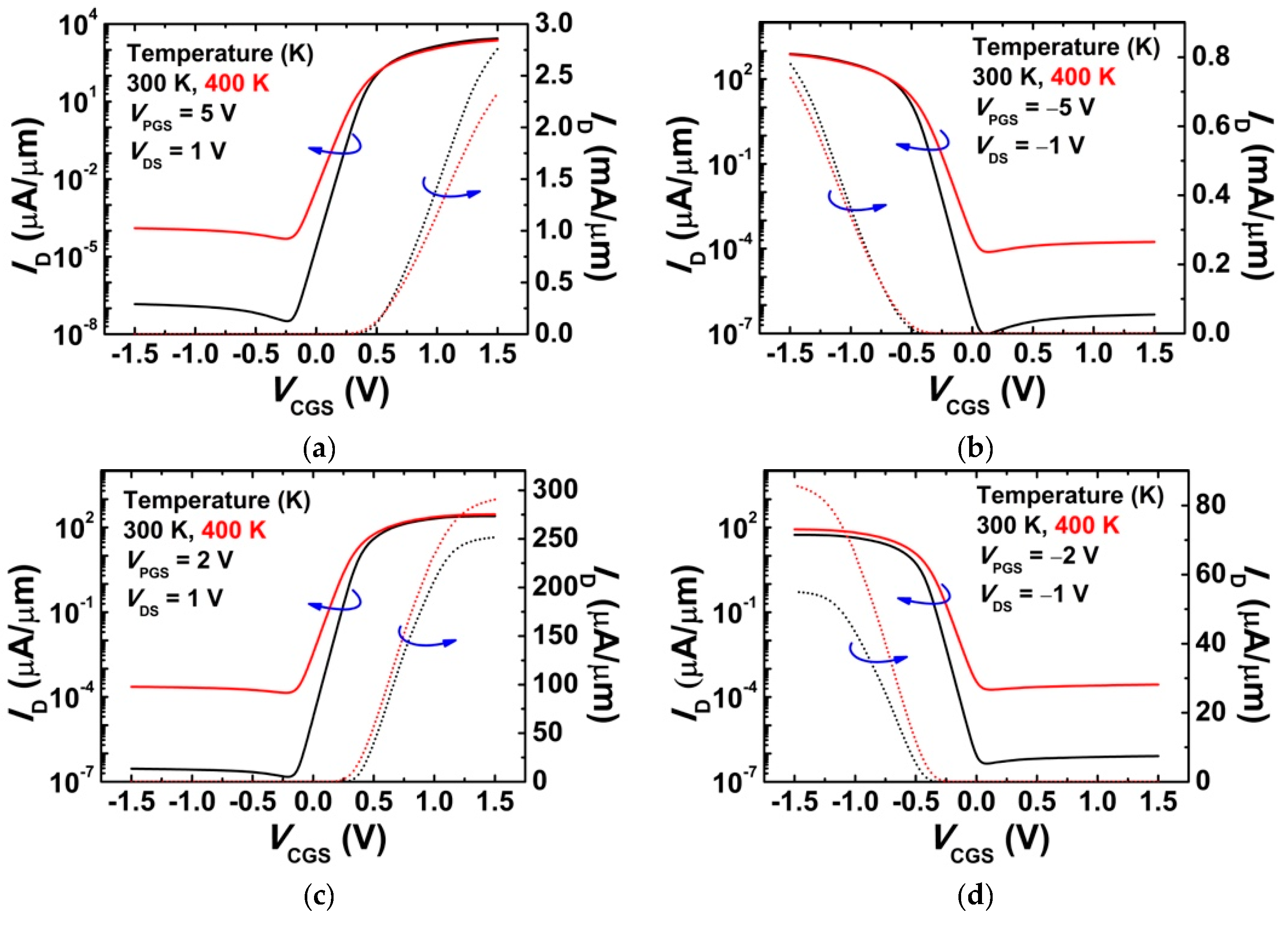
3. Results and Discussion

Figure 2 shows drain current (ID) versus CG bias (VCGS) for n- and p-FET operations as T increases from 300 K to 400 K with different PG bias (VPGS). As shown in Figure 2a,b, the on-current (ION) defined as ID at ±1.5 V-VCGS is decreased for both n- and p-FETs as T increases in accordance with general expectation, since the mobility (μ) is decreased due to phonon scattering as expressed in Equation (1) [16]. The μ at 300 K-T (μ0) and γ are 1417 cm2/V·s and 2.5 for electron, whereas 486 cm2/V·s and 2.2 for hole, respectively [13].
μ = μ 0 ( T 300   K ) γ
The noteworthy points are shown in Figure 2c,d that the ION becomes an increasing function of the T as |VPGS| is decreased from 5 to 2 V.
Figure 3a clearly shows ION has different tendencies on the T depending on the VPGS, regardless of n- or p-FETs. It is not related to the subthreshold characteristics since the extracted S is exactly sitting on the 2.3kB/q-slope (~0.2 mV/K) line similar to the conventional MOSFETs, where kB and q are the Boltzmann constant and elementary charge, respectively (Figure 3b).
In order to analyze these phenomena, the RC-RFET is simply modeled as a channel resistance (RCH) and a Schottky contact resistance (RSC) connected in series, which have an opposite correlation with T. In other words, if T is increased, the RCH is increased due to the increased phonon scattering, whereas the RSC is decreased due to the increased carrier injection ‘over’ and ‘through’ the Schottky barriers at source and drain contacts (Figure 4). Accordingly, the total resistance (RTOT) and ION is dominated by the bigger one. Since RSC is exponentially decreased as a function of band bending, the RTOT can be approximated to RCH and RSC with a small and a large |VPGS|, respectively. From Equation (1), the μ of electron (μe) is more sensitive to T than that of the hole (μh) due to the different coefficient γ. Thus, RCH of n-FET increases faster than that of p-FET as T increase which is well corresponded to the different slopes for 5 V-|VPGS| in Figure 3a. On the other hand, in case of small |VPGS| (= 2V), p-FET is more sensitive than n-FET to the T. This is because the effect of RSC decreasing is cancelled out by the RCH increase with the higher T for n-FET.
In order to confirm the hypothesis, the effects of RSC and RCH on n-FETs’ ION have been examined independently. For that, the change of doping concentration is inappropriate since both factors are affected at the same time. Thus, the RSC and the RCH of n-FET are changed by adjusting SHB and μe, respectively. First, if SBH decreases from 1.06 eV to 0.26 eV, the dominant factor changes from RSC to RCH; ION decreases as T increases as shown in Figure 5. On the other hand, if μe increases several times the default value (1417 cm2/V·s), the RTOT is determined by the RSC (Figure 6). As a result, there is a positive correlation between ION and T. Consequently, the assumption is clearly proven to be reasonable. It has to be mentioned that even if this approach is less practical in terms of device design, it is very meaningful to understand and confirm the operation mechanism and overall physics of RFET which is a milestone for device engineers.

4. Conclusions

The effects of T on the electrical characteristics of RC-RFET have been examined. There is an abnormal phenomenon that the ION decreases as T increases with a small |VPGS|. Based on rigorous study with the help of TCAD simulation, this was attributed to the large RSC which decreases the function of T and dominates the RTOT. This needs to be further addressed for high-performance operation with low-power consumption. In order to decrease SBH for the lower RCH, adopting a narrow band gap material (e.g., SiGe or Ge) at the source/drain and metal contacts could be a promising solution. In future works, the influences of band gap on SBH will be examined and the optimized RC-RFET will be demonstrated.

Author Contributions

Writing (original draft preparation, review, and editing) J.H.K.; supervision, S.K.

Funding

This research was supported in part by the Brain Korea 21 Plus Project, in part by the MOTIE/KSRC under Grant 10080575 (Future Semiconductor Device Technology Development Program), in part by the NRF of Korea funded by the MSIT under Grant NRF-2019M3F3A1A02072091 (Intelligent Semiconductor Technology Development Program) and in part by the MSIT (Ministry of Science and ICT), Korea, under the ITRC (Information Technology Research Center) support program (IITP-2019-2016-0-00309) supervised by the IITP (Institute for Information & communications Technology Planning & Evaluation). The EDA tool was supported by the IC Design Education Center (IDEC), Korea.

Conflicts of Interest

The authors declare no conflicts of interest.

References

  1. Ferain, I.; Colinge, C.A.; Colinge, J.P. Multigate transistors as the future of classical metal-oxide-semiconductor field-effect transistors. Nature 2011, 479, 310–316. [Google Scholar] [CrossRef] [PubMed]
  2. International Roadmap for Devices and Systems (IRDSTM) 2018 Edition. Available online: https://irds.ieee. org/editions/2018 (accessed on 5 October 2019).
  3. Cristoloveanu, S.; Wan, J.; Zaslavsky, A. A review of sharp-switching devices for ultra-low power applications. IEEE J. Electron Devices Soc. 2016, 4, 215–226. [Google Scholar] [CrossRef]
  4. Javey, A.; Tu, R.; Farmer, D.B.; Guo, J.; Gordon, R.G.; Dai, H. High performance n-type carbon nanotube field-effect transistors with chemically doped contacts. Nano Lett. 2005, 5, 345–348. [Google Scholar] [CrossRef] [PubMed]
  5. Trommer, J.; Heinzig, A.; Baldauf, T.; Slesazeck, S.; Mikolajick, T.; Weber, W.M. Functionality-Enhanced Logic Gate Design Enabled by Symmetrical Reconfigurable Silicon Nanowire Transistors. IEEE Trans. Nanotechnol. 2015, 14, 689–698. [Google Scholar] [CrossRef]
  6. Lin, Y.F.; Xu, Y.; Wang, S.T.; Li, S.L.; Yamamoto, M.; Aparecido-Ferreira, A.; Li, W.; Sun, H.; Nakaharai, S.; Jian, W.B.; et al. Ambipolar MoTe2 transistors and their applications in logic circuits. Adv. Mater. 2014, 26, 3263–3269. [Google Scholar] [CrossRef] [PubMed]
  7. Heinzig, A.; Mikolajick, T.; Trommer, J.; Grimm, D.; Weber, W.M. Dually active silicon nanowire transistors and circuits with equal electron and hole transport. Nano Lett. 2013, 13, 4176–4181. [Google Scholar] [CrossRef] [PubMed]
  8. Crupi, G.; Schreurs, D.M.M.P.; Raskin, J.P.; Caddemi, A. A comprehensive review on microwave FinFET modeling for progressing beyond the state of art. Solid. State. Electron. 2013, 80, 81–95. [Google Scholar] [CrossRef]
  9. Crupi, G.; Schreurs, D.M.M.P.; Caddemi, A. Effects of gate-length scaling on microwave mosfet performance. Electronics 2017, 6, 62. [Google Scholar] [CrossRef]
  10. Weber, W.M.; Heinzig, A.; Trommer, J.; Martin, D.; Grube, M.; Mikolajick, T. Reconfigurable nanowire electronics—A review. Solid. State. Electron. 2014, 102, 12–24. [Google Scholar] [CrossRef]
  11. Kim, S.; Kim, S.W. Recessed-channel reconfigurable field-effect transistor. Electron. Lett. 2016, 52, 1640–1642. [Google Scholar] [CrossRef]
  12. Appenzeller, J.; Radosavljević, M.; Knoch, J.; Avouris, P. Tunneling versus thermionic emission in one-dimensional semiconductors. Phys. Rev. Lett. 2004, 92, 4. [Google Scholar] [CrossRef] [PubMed]
  13. Synopsys Inc. Sentaurus Device User Guide-v.K-2015.06; Synopsys Inc.: Mountain View, CA, USA, 2009. [Google Scholar]
  14. Kim, J.Y.; Oh, H.J.; Woo, D.S.; Lee, Y.S.; Kim, D.H.; Kim, S.E.; Ha, G.W.; Kim, H.J.; Kang, N.J.; Park, J.M.; et al. S-RCAT (Sphere-shaped-Recess-Channel-Array Transistor) Technology for 70nm DRAM feature size and beyond. In Proceedings of the Digest of Technical Papers—Symposium on VLSI Technology, Kyoto, Japan, 14–16 June 2005; Volume 2005, pp. 34–35. [Google Scholar]
  15. Park, S.; Seo, H.; Oh, J.; Kim, I.; Hong, H.; Jin, G.; Roh, Y. Roles of residual stress in dynamic refresh failure of a buried-recessed-channel-array transistor (B-CAT) in DRAM. IEEE Electron Device Lett. 2016, 37, 859–861. [Google Scholar] [CrossRef]
  16. Lombardi, C.; Manzini, S.; Saporito, A.; Vanzi, M. A Physically Based Mobility Model for Numerical Simulation of Nonplanar Devices. IEEE Trans. Comput. Des. Integr. Circuits Syst. 1988, 7, 1164–1171. [Google Scholar] [CrossRef]
Figure 1. Schematic structure diagrams for recessed-channel reconfigurable field-effect transistor (RC-RFET). It features the vertically stacked polarity gate (PG) and control gate (CG) separated to each other with an oxide gap.
Electronics 08 01124 g001
Figure 2. Schematic transfer characteristics depending on T with different VPGS. (a) n-FET operations with VPGS = 5 V; (b) p-FET operations with VPGS = −5 V; (c) n-FET operations with VPGS = 2 V; (d) p-FET operations with VPGS = −2 V. The arrows indicate the direction of the graph according to log scale and linear scale.
Electronics 08 01124 g002
Figure 3. Extracted parameters from IDVPGS curves. (a) Normalized ION by ION at 300 K. ION is extracted when VPGS is 1.5 V; (b) subthreshold swing (S). The extracted S is exactly sitting on the 2.3kB/q-slope (~0.2 mV/K) line.
Electronics 08 01124 g003
Figure 4. Energy band diagram and carrier distribution with different T. (a) Low T; (b) high T. The energy band is plotted along the source and channel (Figure 1). The blue-colored areas in the source represent the increased carrier distribution due to the increased T, and blue-colored arrows indicate the increased carriers passing through the Schottky barrier (SB) due to the increased T.
Electronics 08 01124 g004
Figure 5. Normalized ION of n-FET as a function of T with different SBH (Schottky barrier height). The blue arrow shows a decrease in the normalized ID due to SBH reduction.
Electronics 08 01124 g005
Figure 6. Normalized ION of n-FET as a function of T with different μe. The blue arrow shows an increase in the normalized ID due to mobility increasement.
Electronics 08 01124 g006
Table 1. Simulated device parameters.
DefinitionAbbreviationValue
Silicon body thicknessTB20 nm
Gate oxide thickness
Gate length
TOX
LG
1 nm
50 nm
Program gate thickness
Control gate thickness
Oxide thickness between PG and CG
TPG
TCG
TGAP
20 nm
20 nm
10 nm

