Article

Resonant Tunneling Diode (RTD) Terahertz Active Transmission Line Oscillator with Graphene-Plasma Wave and Two Graphene Antennas

1
Department of Microelectronics and Solid-state Electronics, School of Electrical and Information Engineering, Tianjin University, Tianjin 300072, China
2
Department of Microelectronics and Solid-state Electronics, School of Microelectronics, Tianjin University, Tianjin 300072, China
3
Department of Electrical Engineering, Faculty of Engineering, University of Malaya, Kuala Lumpur 50603, Malaysia
4
State Key Laboratory of Precision Measuring Technology and Instruments, Tianjin University, Tianjin 300072, China
*
Author to whom correspondence should be addressed.
Electronics 2019, 8(10), 1164; https://doi.org/10.3390/electronics8101164
Submission received: 14 September 2019 / Revised: 10 October 2019 / Accepted: 11 October 2019 / Published: 14 October 2019
(This article belongs to the Section Microwave and Wireless Communications)

Abstract

:
This study describes the design of a resonant tunneling diode (RTD) oscillator (RTD oscillator) with a RTD-gated-graphene-2DEF (two dimensional electron fluid) and demonstrates the functioning of this RTD oscillator through a transmission line simulation model. Impedance of the RTD oscillator changes periodically when physical dimension of the device is of considerable fraction of the electrical wavelength. As long as impedance matching is achieved, the oscillation frequency is not limited by the size of the device. An RTD oscillator with a graphene film and negative differential resistance (NDR) will produce power amplification. The positive electrode of the DC power supply is modified and designed as an antenna. So, the reflected power can also be radiated to increase RTD oscillator output power. The output analysis shows that through the optimization of the antenna structure, it is possible to increase the RTD oscillator output to 22 mW at 1.9 THz and 20 mW at 6.1 THz respectively. Furthermore, the RTD oscillator has the potential to oscillate at 50 THz with a matching antenna.

1. Introduction

Terahertz (THz) electromagnetic radiation is generally composed of electromagnetic waves with frequencies of 100 GHz–10 THz [1]. The wavelengths of THz waves fall between those of light waves and millimeter waves. They are characterized by strong penetration, high security, and good orientation, and they can be used extensively in medical and exploration applications [2,3]. However, a coherent source with high-power work at room temperature is indispensable for these applications. Terahertz wave sources are classified into optical wave sources and electrical wave sources. Optical THz products have been available commercially [4,5,6,7], but they are expensive and bulky. Resonant tunneling diodes (RTDs) [8,9] are good candidates for electronic THz wave sources from the viewpoint of fabricating resonant tunneling diode oscillator (RTD oscillators). Resonant tunneling diode oscillators are coherent, solid-state, and compact high-power sources with high-power work at room temperature. H. Kanaya et al. [2] reported a 1.42 THz oscillation via a reduction in the RTD intrinsic delay. The same team reported a 1.55 THz oscillation through optimization of the antenna length [10]. A 1.98 THz RTD oscillator was fabricated with the optimum electrode thickness of 2 μm [3]. This is the highest RTD oscillator frequency reported so far. In reference [4], the authors used a conventional lumped-element equivalent circuit to analyze a RTD oscillator. A potential oscillation of 3.0 THz was shown with the RTD and also at 2.8 THz for the integrated device with a slot antenna while the device structure was optimized. However, the theoretical analysis showed that oscillator frequency and RTD size were correlated negatively [4]. By contrary, the device output power and RTD size were correlated positively. Asada, et al. [11] showed in their earlier work, the oscillation frequency increased to 345 GHz with a slot width of 2 mm from a 330 GHz with a slot width of 4 mm. For [3], the oscillation frequency of the RTD Oscillator is already close to 2 THz. At such high frequencies, transmission line theory is more suitable for analyzing RTD Oscillator than the conventional lumped-element equivalent circuit model. Transmission line theory bridges the gap between field analysis and basic circuit theory and therefore is of significant importance in the analysis of microwave even terahertz circuits and devices. The phenomenon of wave propagation on transmission lines can be approached from an extension of circuit theory or from a specialization of Maxwell’s equations [12]. Moreover, the fabrication of high frequency RTD oscillator remains challenging.
In [13], Burke et al. developed the high-frequency transmission line model to describe a metal-gate/insulator/two-dimensional electron fluid (2DEF) structure. Then, the model was used in THz power amplification via plasma wave excitation [14,15], high-electron-mobility transistor (HEMT) with RTD gate [16], and photo-controlled THz amplified modulator [17]. In the previous study, a graphene layer was employed for plasma wave excitation [18,19,20,21]. Optical graphene plasmon resonances were realized spectroscopically with a two-dimensional graphene sheet, and propagating plasmons in real space were resolved directly in experiments.
The study here describes the design of a resonant tunneling diode (RTD) oscillator (RTD oscillator) with a RTD-gated-graphene-two-dimensional electron fluid (2DEF) and demonstrates the functioning of this RTD oscillator through a transmission line model simulation. Firstly, the distributed transmission line model analysis in this study shows that the size of the device is not an indefinite factor affecting the oscillation frequency. The impedance of the device changes periodically when physical dimension of the device is of considerable fraction of the electrical wavelength. As long as impedance matching is achieved, the oscillation frequency is not limited by the size of the device. Therefore, without reducing the frequency, the output power can be greatly increased with the increase of the device size. Secondly, output power increase is not only due to the increase in device size, but also due to a graphene layer which produces RTD-gated-graphene-2DEF and the negative differential resistance (NDR). According to references [14,16,17], two-dimensional electron fluid (2DEF) is required to realize power amplification, which is produced by RTD-gated HEMT with very complicated layered structure. Because the films thickness of the RTD-gated HEMT are very small, only a few nanometers, so the molecular beam epitaxy [19,22,23] or metal–organic chemical vapor deposition [24] is required [25]. They are complex and expensive processes. Due to the graphene plasma phenomenon, two-dimensional electron fluid (2DEF) is generated by a graphene film instead of RTD-gated HEMT, reducing the difficulty of implementing the RTD oscillator. Thirdly, transmission lines model in this study shows that power reflection cannot be completely eliminated, both in theory and in practical applications. This is especially when impedance matching is not satisfied, power reflection and loss would be large. A DC bias is needed to make the device work normally. RTD requires two electrodes and oscillator requires an antenna. Refer to [2,3,10] and [26], it is common to apply a DC bias voltage to the antenna. In this study, the positive electrode of the DC power supply is modified and designed as an antenna. So, the reflected power can also be radiated to increase RTD oscillator output power. In this study, the Authors demonstrated RTD oscillator could output power of 22 mW at 1.9 THz and 20 mW at 6.1 THz respectively.

2. Modeling

A RTD is a semiconductor that exhibits controllable negative difference resistance (NDR) regions. The N-shaped I-V characteristics [27,28] of RTDs provide electrical gain for THz oscillator at room temperature [14]. A RTD is realized via the creation of a double-barrier quantum well (DBQW) structure [26] comprising a narrow-bandgap material sandwiched between two thin slabs of a wide-bandgap material. However, the results of a theoretical analysis show that oscillator frequency and RTD size are negatively correlated [4]. In this study, a graphene layer is fabricated before the sandwich structure, and the graphene layer forms a RTD-gated-graphene-2DEF. The developed RTD oscillator realizes power amplification via a graphene-plasma wave layer [17]. As shown in Figure 1a,b, a RTD oscillator comprises a RTD, RTD-gated-graphene-2DEF and two graphene antennas. As shown in Figure 1b, the length of a transmission line is equal to the channel length L, which includes a RTD and a RTD-gated-graphene-2DEF.As shown in Figure 1b, a distributed circuit model is established to represent the contributions of NDR and 2DEF to a RTD-gated-graphene-2DEF oscillator. The RTD oscillator is biased by the application of dc voltage to the left antenna [29].
Electrical size is key difference between transmission line model and lumped-element equivalent circuit model [12]. It assumes that circuit analysis works when physical dimension of the device is much smaller than the electrical wavelength, while transmission lines model works when physical dimension of the device is a considerable fraction of the electrical wavelength. Electrical wavelength is wavelength of alternating current signals, which is defined as λ = c/f, where c is speed of light, f is frequency of alternating current signal. Electrical size is defined as k = W/λ, where W = 10 µm is the RTD width in this study [12]. The oscillator frequency ranges from 1 THz to 10 THz, 1/30 ≤ k ≤ 1/3. A transmission line model is a network with distributed parameters, where currents and voltages vary in magnitude and phase over its length. Current and voltage of conventional lumped-element equivalent circuit do not vary appreciably over the size of the device.
As shown in Figure 1b,c, transmission line model is represented as a two-wire line since transmission lines always have at least two conductors. The following parameters are used to describe the distributed circuit model of a transmission line: r is series resistance per unit length, for both conductors, in Ω/cm, c is shunt capacitance per unit length, in F/cm, g is shunt conductance per unit length, in S/cm, l is series inductance per unit length, for both conductors, in H/cm.
These parameters are defined as [12,14,16,17]
r = 1 e μ n s W
c = c 0 W
g = g 0 W = W d I d V
l = m e 2 μ n s W
where e is the electronic charge, in 1.6*10−19 C; µ is the electron mobility in the transmission line, in cm2V−1s−1; W the RTD width, in cm; m* is the electron effective mass, in kg; ns is the 2DEF sheet charge density, in cm−2; g0 is the gate conductance per unit area, in S/cm2; and c0 is the gate capacitance per unit area, in F/cm−2. The complex propagation constant γ of the transmission line model is defined as [12]
γ = ( r + j ω l ) ( g + j ω c ) = α + j β
where ω is the angular frequency. The characteristic impedance Z0 is defined as [26]
Z 0 = r + j ω l g + j ω c
Figure 1 Equivalent active transmission line oscillator model shows a length L of a lossy transmission line terminated in a right antenna impedance ZANT. Thus, γ = α + jβ is complex, but Z0 is approximately real when we assume the loss is small. The expressions for current and voltage wave on the lossy line are.
I ( z ) = V 0 + Z 0 [ e γ z Γ e γ z ]
V ( z ) = V 0 + [ e γ z Γ e γ z ]
As shown in Equations (7) and (8), where Γ is the reflection coefficient of the load. At z = 0, V0+ is the incident voltage amplitude. At a distance L from the load, the reflection coefficient is
Γ ( L ) = V 0 e j β L V 0 + e j β L e 2 α L = Γ ( 0 ) e 2 α L e 2 j β L = e 2 γ L
Γ(0) is the reflection coefficient at z = 0, as
Γ ( 0 ) = V 0 V 0 + = Z A N T Z 0 Z A N T + Z 0
According to axis z1, the impedance Zin toward the right of the transmission line model of RTD oscillator is as
Z i n = V ( L ) I ( L ) = Z 0 Z A N T + j Z 0 tanh γ L Z 0 + j Z A N T tanh γ L
The impedance of the left antenna is Z’ANT. According to axis z2, the impedance Z’in toward the left is
Z i n = V ( L ) I ( L ) = Z 0 Z A N T + j Z 0 tanh γ L Z 0 + j Z A N T tanh γ L
In this study, two antennas of the same size were designed. The impedances ZANT and Z’ANT are equal, and the impedances Zin and Z’in are equal.
Z A N T = Z A N T
Z i n = Z i n
To ensure that the oscillator works, Equation (15) must be satisfied as following
R e ( Z i n ) + R e ( Z A N T ) = 0
Re(Zin) is the real part of Zin, and Re(Z’ANT) is the real part of Z’ANT. I-V characteristic of RTD which was simulated by WINGREEN is shown in Figure 1d. This is a N-type NDR, and g is called negative difference conductor (NDC) which is defined as [16]
g = Δ I Δ V = I P I V V P V V
where IP is peak current density, IV is valley current density, VP is peak voltage, VV is valley voltage. As shown in Figure 1d, ∆I = 29 mA/µm2 and ∆V = 0.7 V. The RTD oscillator is biased at 0.7 V at NDR region. According to reference [14,16,17], Equation (3) can be assumed as
g = −rc/l
The load achieves the maximum power transmission when the loaded impedance ZANT and power source internal resistance Z’in for conjugate match in sine stable state electric circuit. To achieve the maximum power transmission, stable oscillation should satisfy the following condition.
Z i n = Z A N T
According to Equations (14)–(18), to achieve the maximum power transmission, Re(Zin) and Re(Z’ANT) must be equal as well. So, Re(Zin) must equals to “zero”, as shown in Figure 2 and Figure 3.
R e ( Z i n ) = R e ( Z A N T ) = 0
GT denotes transducer power gain. Because of the plasma wave in the RTD-gated-graphene-2DEF and the negative differential conductance (NDC) of the RTD, according to the transmission line theory, the oscillator works and amplifies THz waves in the channel [13], as
G T = P L P a v s = | S 22 | 2 ( 1 | Γ S | 2 ) ( 1 | Γ L | 2 ) | 1 Γ S Γ i n | 2 | 1 S 22 Γ L | 2
where PL is the power transmitted to the load, and Pavs is the power available from the source, which is the maximum power that can be supplied to the transmission line. S11 is the return loss, and S21 is the transmission gain. ΓS and ΓL are the source reflection coefficient and the load reflection coefficient, respectively. Assuming no reflection, ΓS = ΓL = 0, and Equation (20) can be simplified as
G T = | S 21 | 2
In Equations (20) and (21), [14]
S 11 = S 22 = ζ sinh ( γ L ) ζ 1 sinh ( γ L ) 2 cosh ( γ L ) + sinh ( γ L ) ( ζ + ζ 1 )
S 12 = S 21 = 2 2 cosh ( γ L ) + sinh ( γ L ) ( ζ + ζ 1 )
ζ = Z A N T Z 0
where the complex quantity ζ is defined as the ratio of the plasma-wave-transmission-line impedance over the source impedance. The angular frequency ω and Equation (5) can be rewritten as
ω = π 2 4 L 2 l c r 2 l 2
γ = r 2 c l ( π 2 4 L 2 l c r 2 l 2 ) c l = π 2 4 L 2 = ± j π 2 L
Therefore, Equation (20) can be rewritten as Equation (27) [14]
G T = 4 | 2 cosh ( γ L ) + sinh ( γ L ) ( ζ + ζ 1 ) | 2 = 4 | ( ζ + ζ 1 ) | 2
NDC is a fundamental factor to provide power gain under these circumstances. By inspecting (5), (6) and (27), in order to ensure at least 6 dB of power gain, 0 < (ωl/r) < (1/3) must be satisfied.
As shown in Figure 2 and Figure 3, Re (Zin) could be zero. However, the real part of ZANT is greater than zero at all times, as shown in Figure 4f. Therefore, the right antenna cannot achieve the maximum power transmission. Consequently, RTD oscillator power is reflected toward the left. The left antenna receives the reflected power and radios it outward. As a result, the proposed RTD oscillator can achieve significantly higher power output than a traditional RTD oscillator.

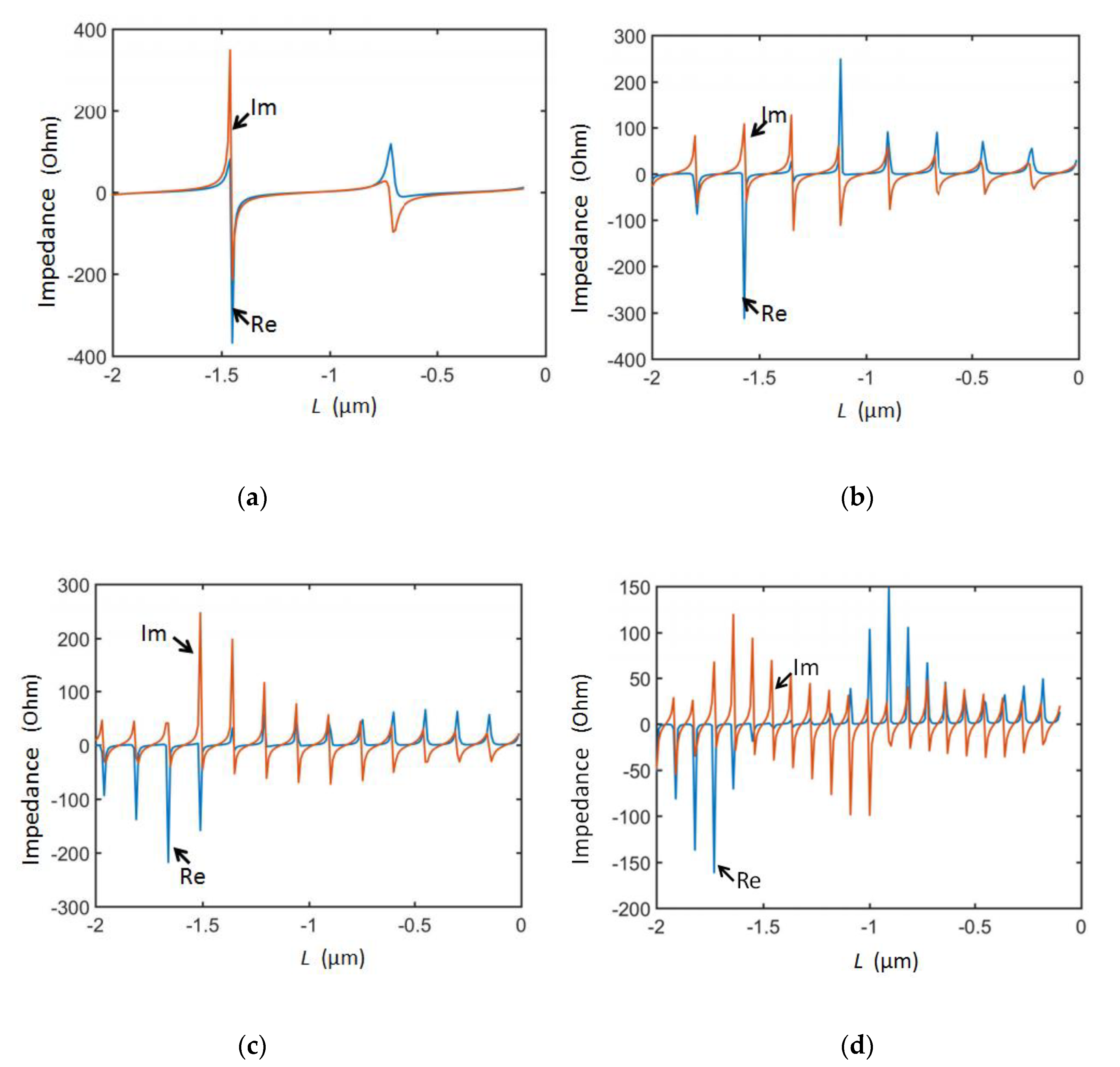
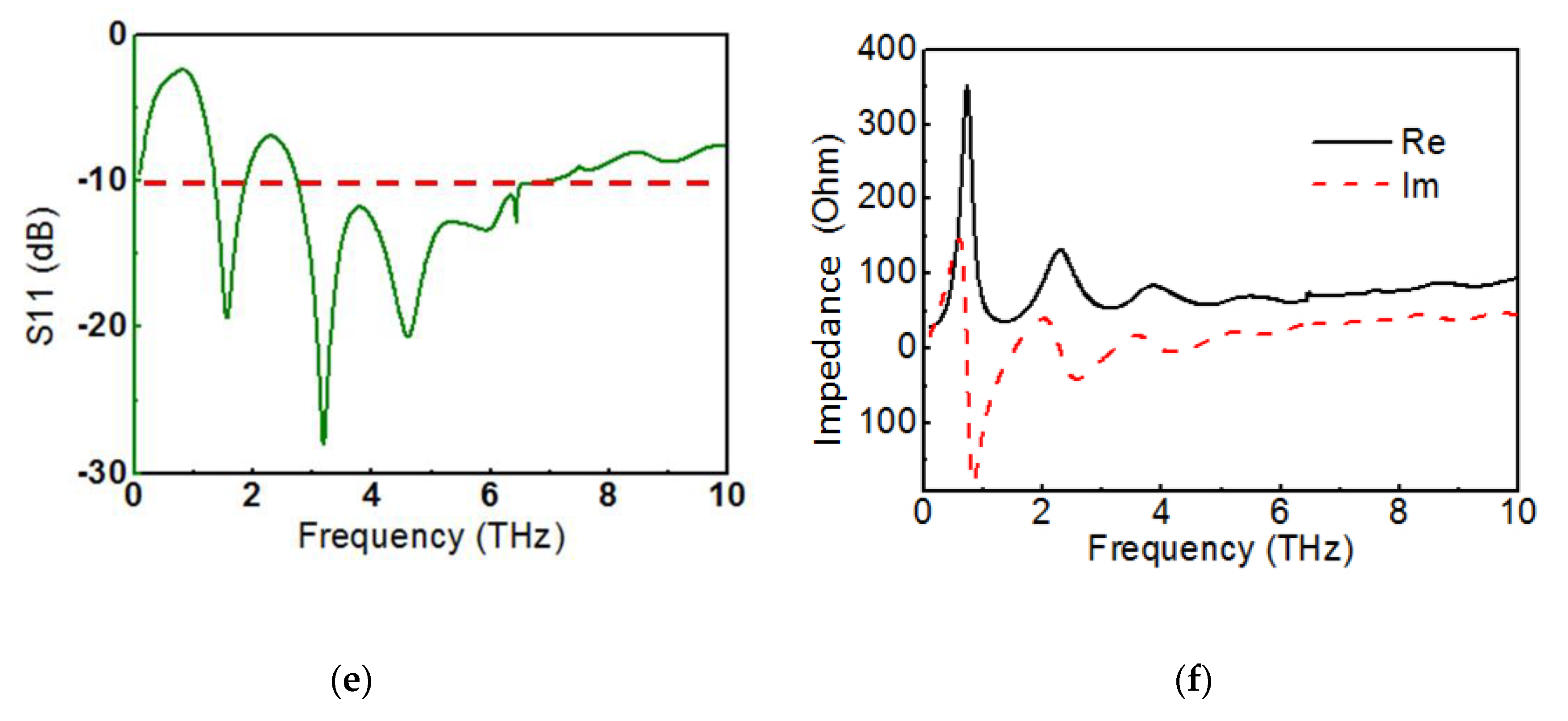
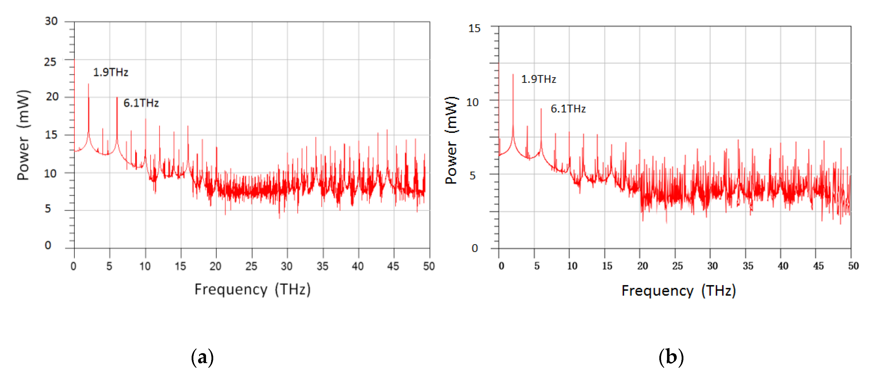
3. Simulation and Discussion

Structural parameters in the transmission line are listed in Table 1. Figure 2 shows the relationship between the impedance and the frequency of the RTD oscillator, as derived using the transmission line model. Although the gate length of RTD is changed from 1 μm to 2 μm, the impedance Zin or Z’in varies periodically with the RTD oscillator frequency. Figure 3 shows that a certain impedance Zin or Z’in is obtained at certain RTD lengths. When the antenna impedance satisfies Equation (15), the RTD oscillator can work at multiple frequencies. To realize higher output power, the gate length must be increased. According to Equations (1)–(12) and Figure 3, increasing the gate width and the gate length of the RTD do not affect its oscillation frequency in the distributed model simulation.
As shown in Figure 4a, the two antennas in Figure 1a were designed with the same size. Figure 4b shows that the antenna gain of single antenna is –13.373 dB. In Figure 1c, the axial ratio value of this antenna is 38 dB when theta is 0, so polarization of the antenna is linear polarization. Figure 4d shows that the antenna gain of two antennas is –10.968 dB, which is lower than that of a regular patch antenna, because the antenna has two ultrawide bands. Antenna gain of two antennas is higher than that of single antenna. Figure 4e shows the S11 of the graphene antenna. When S11 < 10 dB, the antenna bands are 1.37–1.93 THz and 2.75–7.00 THz. Figure 4f shows the impedance of the graphene antenna.
In fact, the output power of the existing RTD oscillator terahertz source is very small, which is the main reason for its limited application. The antenna used in the prior literature is slot antenna, which is complicated in manufacturing process and is not suitable for integration with other devices and mass production. Although the graphene antenna designed in the present study has a low gain, due to the RTD-gated-graphene-2DEF of the RTD oscillator, its output power is very high. A DC bias is necessary to make the device work normally. This requires an electrode and an antenna. Refer to [2,3,10] and [26], it is common to apply a DC bias voltage to the antenna. In this study, the positive electrode of the DC power supply is modified and designed as an antenna. So, the reflected power can also be radiated to increase RTD oscillator output power.
Advanced Design System (ADS, Keysight Technologies) was used to simulate the fully distributed active transmission line RTD-gated-graphene-2DEF THz oscillator in this study. As shown in Figure 5, the oscillation consists of the first and higher harmonics. The harmonic power is defined per Equations (28) to (31)
Γ = Z A N T Z 0 Z A N T + Z 0
where Г denotes the voltage reflection coefficient.
The maximum output power P of the transmission line can be rewritten as
| Γ ( L ) | = Γ e 2 γ L
α = Re { γ }
P = 1 2 Re { V ( L ) I ( L ) } = | V 0 + | 2 2 Z 0 [ 1 | Γ ( L ) | 2 ] e 2 α L
V0+ is the power voltage. The generation of harmonics, including the odd harmonics, can be described by solving Equation (32)
f = 1 + 2 k 4 m c 0 e 2 μ n s L , k = 0 , 1 , 2 ,
As shown in Figure 5, the power of the first harmonic is higher than that of the higher harmonics. When the device dimensions are L = 2 µm and W = 10 µm, the power of the first harmonic is 22 mW at 1.9 THz and that of the higher harmonics is 20 mW at 6.1 THz. When the device dimensions are L = 1 µm and W = 10 µm, the power of the first harmonic is 11.75 mW at 1.9 THz and that of the higher harmonics is 9.5 mW at 6.1 THz. These results show that the RTD oscillator power increases as its size increases, but its frequency is not affected. Because of the mismatch between Z’in and the right antenna, the RTD oscillator power is reflected toward the left antenna. The left antenna receives the reflected power and radiates it outward. With two graphene antennas, the device radiates high harmonics to provide high-frequency THz waves.

4. Conclusions

The study herewith, described the design of a RTD oscillator with a RTD-gated-graphene-2DEF and demonstrated the functioning of this RTD oscillator through a fully distributed transmission line simulation model. This simulated work has developed the two main parts of the RTD Oscillator, the RTD and antenna. Amplification arising from the dynamics of electron plasma waves in a high electron mobility transistor (HEMT) channel with injection from the gate exhibiting negative differential resistance (NDR). In this paper, HEMT is replaced by a graphene layer, which has been proven to produce electron plasma. This study has proven that the impedance of the device changes periodically when the RTD electrical size 1/30 ≤ k ≤ 1/3. As long as the impedance matching is achieved, the oscillation frequency is not limited by the size of the device. Therefore, without reducing the frequency, the output power can be greatly increased with the increase of the device size. At the same time, the graphene antenna provides two ultra-wide bands which are 1.37–1.93 THz and 2.75–7.00 THz. Because of the mismatch between Z’in and the right antenna, RTD oscillator power is reflected toward and radiated outward from the left antenna. Therefore, the proposed RTD oscillator can generate significantly higher levels of power than traditional RTD oscillators. With two graphene antennas, the device can radio high harmonics to provide RTD oscillator output powers of 22 mW at 1.9 THz and 20 mW at 6.1 THz. The results of this research study can serve as a fundamental principle in the fabrication of a THz RTD oscillator.

Author Contributions

Methodology, investigation, resources, and data curation, F.Z. and C.Z.; conceptualization, supervision, project administration, and funding acquisition, W.G.; validation, J.C.; writing—original draft preparation, writing—review and editing and visualization, C.A.T.H.T, L.S. and Y.Z.

Funding

This work was supported by the National Natural Science Foundation of China (No. 61331003).

Conflicts of Interest

The authors declare no conflict of interest.

References

  1. Choe, W.; Jeong, J. A Broadband THz On-Chip Transition Using a Dipole Antenna with Integrated Balun. Electronics 2018, 7, 236. [Google Scholar] [CrossRef]
  2. Kanaya, H.; Sogabe, R.; Maekawa, T.; Suzuki, S.; Asada, M. Fundamental Oscillation up to 1.42 THz in Resonant Tunneling Diodes by Optimized Collector Spacer Thickness. J. Infrared Millim. Terahertz Waves 2014, 35, 425–431. [Google Scholar] [CrossRef]
  3. Izumi, R.; Suzuki, S.; Asada, M. 1.98 THz resonant-tunneling-diode oscillator with reduced conduction loss by thick antenna electrode. In Proceedings of the IEEE 2017 42nd International Conference on Infrared, Millimeter, and Terahertz Waves (IRMMW-THz), Cancun, Mexico, 27 August–1 September 2017; pp. 1–2. [Google Scholar] [CrossRef]
  4. Orihashi, N.; Hattori, S.; Suzuki, S.; Asada, M. Experimental and Theoretical Characteristics of Sub-Terahertz and Terahertz Oscillations of Resonant Tunneling Diodes Integrated with Slot Antennas. Jpn. J. Appl. Phys. 2005, 44, 7809–7815. [Google Scholar] [CrossRef]
  5. Li, C.H.; Chiu, T.Y. 340-GHz Low-Cost and High-Gain On-Chip Higher Order Mode Dielectric Resonator Antenna for THz Applications. IEEE Trans. Terahertz Sci. Technol. 2017, 7, 284–294. [Google Scholar] [CrossRef]
  6. TeraView, TeraPulse Lx. Available online: http://www.teraview.com/products/TeraPulse%204000/index.html (accessed on 13 September 2019).
  7. TOPTICA Photonics, Terahertz Systems Optoelectronic Terahertz-Generation. Available online: https://www.toptica.com/products/terahertz-systems/ (accessed on 13 September 2019).
  8. Wasige, E.; Alharbi, K.H.; Alkhalidi, A.; Wang, J.; Khalid, A.; Rodrigues, G.C.; Figueiredo, J. Resonant tunnelling diode terahertz sources for broadband wireless communications. In Terahertz, RF, Millimeter, and Submillimeter-Wave Technology and Applications X; Society of Photo-optical Instrumentation Engineers: Bellingham, WA, USA, 2017; p. 101031J. [Google Scholar] [CrossRef]
  9. Oshima, N.; Hashimoto, K.; Horikawa, D.; Suzuki, S.; Asada, M. Wireless data transmission of 30 Gbps at a 500-GHz range using resonant-tunneling-diode terahertz oscillator. In Proceedings of the 2016 IEEE MTT-S International Microwave Symposium (IMS), San Francisco, CA, USA, 22–27 May 2016; pp. 1–4. [Google Scholar] [CrossRef]
  10. Maekawa, T.; Kanaya, H.; Suzuki, S.; Asada, M. Frequency increase in terahertz oscillation of resonant tunnelling diode up to 1.55 THz by reduced slot-antenna length. Electron. Lett. 2014, 50, 1214–1216. [Google Scholar] [CrossRef]
  11. Asada, M.; Suzuki, S.; Kishimoto, N. Resonant tunneling diodes for sub-terahertz and terahertz oscillators. Jpn. J. Appl. Phys. 2008, 47, 4375. [Google Scholar] [CrossRef]
  12. Pozar, D.M. Microwave Engineering, 4 ed.; Wiley: Hoboken, NJ, USA, 2012; pp. 1–48. [Google Scholar]
  13. Burke, P.J.; Spielman, I.B.; Eisenstein, J.P.; Pfeiffer, L.N.; West, K.W. High frequency conductivity of the high-mobility two-dimensional electron gas. Appl. Phys. Lett. 2000, 76, 745–747. [Google Scholar] [CrossRef]
  14. Sensale-Rodriguez, B.; Lei, L.; Fay, P.; Jena, D.; Xing, H.G. Power amplification at THz via plasma wave excitation in RTD-gated HEMTs. IEEE Trans. Terahertz Sci. Technol. 2013, 3, 200–206. [Google Scholar] [CrossRef]
  15. Sensale-Rodriguez, B. Graphene-insulator-graphene active plasmonic terahertz devices. Appl. Phys. Lett. 2013, 103, 123109. [Google Scholar] [CrossRef] [Green Version]
  16. Mao, X.; Xie, S.; Zhu, C.; Geng, Z.; Chen, H. Theoretical study of terahertz active transmission line oscillator based on RTD-gated HEMT. AIP Adv. 2018, 8, 065323. [Google Scholar] [CrossRef]
  17. Zhu, C.; Mao, L.; Zhao, F.; Mao, X.; Guo, W. Photo-Controlled Terahertz Amplified Modulator via Plasma Wave Excitation in ORTD-gated HEMTs. IEEE Photonics J. 2017, 9, 1–8. [Google Scholar] [CrossRef]
  18. Chen, J.; Badioli, M.; Alonso-González, P.; Thongrattanasiri, S.; Huth, F.; Osmond, J.; Spasenović, M.; Centeno, A.; Pesquera, A.; Godignon, P. Optical nano-imaging of gate-tunable graphene plasmons. Nature 2012, 487, 77. [Google Scholar] [CrossRef] [PubMed]
  19. Fei, Z.; Rodin, A.S.; Andreev, G.O.; Bao, W. Gate-tuning of graphene plasmons revealed by infrared nano-imaging. Nature 2012, 487, 82. [Google Scholar] [CrossRef] [PubMed]
  20. Thongrattanasiri, S.; Manjavacas, A.; de Abajo, F.J.G. Quantum Finite-Size Effects in Graphene Plasmons. ACS Nano 2012, 6, 1766–1775. [Google Scholar] [CrossRef] [Green Version]
  21. Cox, J.D.; Silveiro, I.; de Abajo, F.J.G. Quantum Effects in the Nonlinear Response of Graphene Plasmons. ACS Nano 2016, 10, 1995–2003. [Google Scholar] [CrossRef] [Green Version]
  22. Dasgupta, S.; Nidhi, Brown, D.F.; Wu, F.; Keller, S.; Speck, J.S.; Mishra, U.K. Ultralow nonalloyed Ohmic contact resistance to self aligned N-polar GaN high electron mobility transistors by In(Ga)N regrowth. Appl. Phys. Lett. 2010, 96, 3. [Google Scholar] [CrossRef]
  23. Green, A.J.; Gillespie, J.K.; Fitch, R.C.; Walker, D.E.; Lindquist, M.; Crespo, A.; Brooks, D.; Beam, E.; Xie, A.; Kumar, V.; et al. ScAlN/GaN High-Electron-Mobility Transistors With 2.4-A/mm Current Density and 0.67-S/mm Transconductance. IEEE Electron Device Lett. 2019, 40, 1056–1059. [Google Scholar] [CrossRef]
  24. Wang, R.H.; Saunier, P.; Xing, X.; Lian, C.X.; Gao, X.A.; Guo, S.P.; Snider, G.; Fay, P.; Jena, D.; Xing, H.L. Gate-Recessed Enhancement-Mode InAlN/AlN/GaN HEMTs With 1.9-A/mm Drain Current Density and 800-mS/mm Transconductance. IEEE Electron Device Lett. 2010, 31, 1383–1385. [Google Scholar] [CrossRef]
  25. Guo, J.; Li, G.; Faria, F.; Cao, Y.; Wang, R.; Verma, J.; Gao, X.; Guo, S.; Beam, E.; Ketterson, A.; et al. MBE-Regrown Ohmics in InAlN HEMTs With a Regrowth Interface Resistance of 0.05 Omega mm. IEEE Electron Device Lett. 2012, 33, 525–527. [Google Scholar] [CrossRef]
  26. Wang, J.; Al-Khalidi, A.; Zhang, W.; Wasige, E.; Kelly, A.E.; Watson, S.; Cantu, H.; Figueiredo, J. Resonant tunneling diode oscillators for optical communications. In Third International Conference on Applications of Optics and Photonics; International Society for Optics and Photonics: Bellingham, WA, USA, 2017. [Google Scholar] [CrossRef] [Green Version]
  27. Cong, J.; Mao, L.; Xie, S.; Zhao, F.; Yan, D.; Guo, W. Photoelectric Dual Control Negative Differential Resistance Device Fabricated by Standard CMOS Process. IEEE Photonics J. 2019, 11. [Google Scholar] [CrossRef]
  28. Yang, C.C. Influence of Parasitic Effects in Negative Differential Resistance Characteristics of Resonant Tunneling. Electronics 2019, 8, 673. [Google Scholar] [CrossRef]
  29. Shanawani, M.; Masotti, D.; Costanzo, A. THz Rectennas and Their Design Rules. Electronics 2017, 6, 99. [Google Scholar] [CrossRef]
  30. Suzuki, S.; Shiraishi, M.; Shibayama, H.; Asada, M. High-Power Operation of Terahertz Oscillators with Resonant Tunneling Diodes Using Impedance-Matched Antennas and Array Configuration. IEEE J. Sel. Top. Quantum Electron. 2013, 19, 8500108. [Google Scholar] [CrossRef]
  31. Suzuki, S.; Teranishi, A.; Hinata, K.; Asada, M. Fundamental oscillation up to 831 GHz in GaInAs/AlAs resonant tunneling diode. In Proceedings of the 2009 IEEE International Conference on Indium Phosphide & Related Materials, Newport Beach, CA, USA, 10–14 May 2009. [Google Scholar] [CrossRef]
Figure 1. (a) Top view of resonant tunneling diode (RTD) terahertz oscillator. The developed oscillator comprises a RTD, RTD-gated-graphene-2DEF, and two graphene antennas. (b) Cross-section of RTD terahertz oscillator. Distributed transmission line model of RTD-gated-graphene-2DEF (two dimensional electron fluid) RTD oscillator. (c) Equivalent active transmission line oscillator model. (d) I-V characteristic of the RTD.
Electronics 08 01164 g001
Figure 2. Relationship between impedance and frequency of transmission line: (a) Zin or Z’in (L = 1 μm) and (b) Zin or Z’in (L = 2 μm).
Electronics 08 01164 g002
Figure 3. Relationship between impedance Zin or Z’in and length of transmission line. (a) Frequency = 0.1 THz, (b) frequency = 1 THz, (c) frequency = 6 THz, and (d) frequency = 10 THz.
Electronics 08 01164 g003
Figure 4. (a) Structure of graphene antenna (WA is the width of the radiation patch, and LA is the length of the patch. Wg is the width of the ground plan, Lg the length of the ground, Win the width of the slot, Lin the length of the slot, W1 the width of the micro-strip line, and L1 the length of the micro-strip line), (b) antenna gain of single antenna, (c) axial ratio value, (d) antenna gain of two antennas, (e) S11, and (f) impedance of graphene antenna.
Electronics 08 01164 g004aElectronics 08 01164 g004b
Figure 5. Power spectrum of oscillator: (a) Device dimensions are L = 2 µm and W = 10 µm. (b) Device dimensions are L = 1 µm and W = 10 µm.
Electronics 08 01164 g005
Table 1. Structural parameters in the transmission line [30,31].
ParametersValue
Electron Mobility μ27,000 cm2V−1s−1
Electron Effective Mass m*0.04m0
2DEG Sheet Electron Density ns1012 cm−2
RTD width W10 μm

