Abstract
Air-gap (AG) technology on back-end-of-line (BEOL) provides a means to improve performance without area or power degradation. However, the “blind” use of AG based on traditional design methodologies does not provide sufficient performance gain. We developed an AG-aware design methodology to maximize performance gain with minimum cost. The experimental results of the proposed methodology, which was tested using a 10 nm Advanced RISC Machine (ARM) Cortex-A9 quad-core central processing unit (CPU), indicated a performance gain of 6.1–8.4% compared with traditional AG design. The performance gain achieved represents about half of the 10–15% performance improvement under the same power by a process node shrink. A Si process of consecutive double AG layers was developed by overcoming various process challenges, such as AG depth control, Cu/ultra-low-k damage, the hermetic AG liner, and step-height control above the AG. Furthermore, the capacitance was reduced by 17.0%, which satisfied the target goal in the simulation stage for the assumed structure. The optimized integration process was validated according to the function yield of the CPU, which was comparable to that of a non-AG process. The time-dependent dielectric breakdown and electromigration lifetime of the AG wire satisfied the 10-year criteria, and the assembly yield was verified.
1. Introduction
The scaling of large-scale integration technology has significantly increased the parasitic resistance and capacitance in multilevel interconnects. With regard to capacitance, low-k materials are widely used as intermetal dielectrics (IMDs) and interlayer dielectrics to enhance circuit performance and reduce power consumption [1,2]. However, the use of low-k materials is challenging owing to their mechanical strength and process immunity properties, which are degraded with the reduction of the k-value [3]. This is generally caused by breakage of the strong Si-O network through Si-CH3 termination, yielding low permittivity, and by the introduction of tiny pores in the matrix, which allow air to enter the dielectric material [4,5]. The ultimate solution for a low k-value is the exclusion of all materials from the IMD, which is called an air gap (AG). There are two types of AG processes: (1) removal of the sacrificial material via thermal decomposition or chemical treatment [6,7,8,9,10] through the upper dielectric layer and (2) etching back the IMD followed by pinch-off of the next IMD deposition [11,12,13,14,15]. In the latter case, the AG can be formed selectively at the critical path, leaving dielectric materials in other places, which can retain the mechanical strength.
Among the various design techniques for optimizing interconnects, wire sizing and spacing have been widely studied since the early 1990s and have been effectively applied to high-performance designs. Wire sizing and spacing for single and multiple nets based on the Elmore delay are addressed in [16]. Wire width optimization in a clock tree was studied in [17], electromigration (EM)-constrained wire-sizing methods were investigated in [18], and noise-driven wire sizing was examined in [19]. However, design approaches such as wire sizing and spacing lead to an area penalty [20]. AG technology provides a means to improve the performance without area or power degradation. Nevertheless, an AG cannot be generated for all metal layers or all nets, because of manufacturing limitations and cost increments. Thus, naïve approaches that do not consider the design context do not substantially improve the design quality.
In this paper, we propose a novel AG-aware design methodology to maximize the performance with minimum cost. We also present the necessary process enhancements for reliable manufacturability, with Si validation results. The main contributions of our work are summarized as follows:
- We present an analytical method for estimating the performance gain by applying an AG. According to this analytical method, an optimal set of metal-layer combinations to apply the AG is provided.
- An AG-aware physical design methodology for maximizing the performance with minimum cost is developed. The proposed methodology can be used in commercial placement and routing tools and provides a performance gain of 6.1–8.4% compared with traditional AG design.
- We present a highly manufacturable AG process to perform Si validation by overcoming various process challenges and achieve consecutive AG layers. We prove the feasibility of the AG process by the central processing unit (CPU) chip yield, packaging, and interconnect reliability, e.g., the time-dependent dielectric breakdown (TDDB) and EM.
2. Challenges
2.1. Performance Gain and Process Cost
We applied AGs to the 10 nm Advanced RISC Machine (ARM) Cortex-A9 (CPU10-A) in a premium mobile processor, which was implemented with three 48 nm-pitch (p48) and four 80 nm-pitch (p80) layers. Figure 1 shows the performance gain and process cost with respect to the number of applied AG layers. At least two metal layers had to be assigned for the AG to complete routing via horizontal and vertical connections. The M1 layer was not used for signal routing. The performance improved by only 0.6% with two AG layers, whereas a 2.2% performance gain was observed when the AG was applied to all six routing metal layers. The process cost of six AG layers was 6.0% higher than that of the minimum two AG layers.
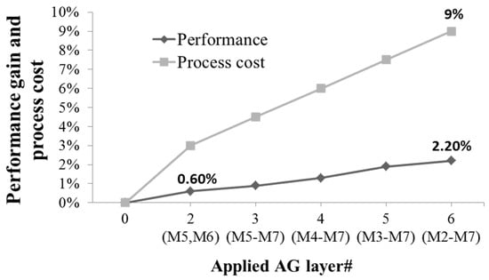
Figure 1.
Performance gain and process cost with respect to the number of applied air gap (AG) layers.
We verified the AG performance gain for the CPU10-A by assessing the impact of the AG with a simple circuit (TC1) consisting of three timing paths. We evaluated two routing structures: one with a 100.0% AG portion and the other with 50.0%. The circuit simulation results revealed a performance gain of 15.0% and a capacitance gain of 17.0% with the 100.0% AG portion, as well as a performance gain of 9.0% and capacitance gain of 12.0% with the 50.0% portion. The large performance-gain gap between the CPU10-A and the TC1 implies that there are practical limitations that restrict the performance gain due to AGs in real designs. According to our analysis, we summarize the factors limiting AG performance gain in real designs as follows:
- Because fine-pitched lower metal levels consist of many short lines with many vias, the chances to apply an AG are extremely limited owing to the AG design rule restrictions at the line-end and upper via.
- Actual nets are dispersed on many routing layers and thus only part of the net benefits from the AG.
Chip performance is characterized by the worst negative slack. If the routing structure of the nets on the most timing-critical path is inadequate for the AG—e.g., lower metal levels or metal layers where the AG cannot be applied—the slack of the most timing-critical path is not improved, and the performance gain is small even though many other timing-critical paths are significantly improved.
2.2. Integration Process
The schematic process flow of the AG is shown in Figure 2. The AG process starts after Cu chemical mechanical polishing (CMP) of the target layer using conventional dual-damascene (DD) technology. The IMD is recessed using a hard mask (HM), which is patterned by an additional photomask for the AG. The HM open area covers one or more spaces, and two edges of the HM sit on the Cu metal line. In the HM open area, only the IMD sandwiched with Cu lines are etched away in a self-aligned manner. The AG liner covers the whole surface, including the recessed pattern, and the following IMD deposition closes the AG via pinch-off at the top of the IMD recess. Then, the process moves back to the conventional Cu DD to build the next metal level. Thus, the AG process is simply plugged into the conventional Cu DD process, between Cu-CMP and IMD deposition, with one additional mask. Because AG patterning is a self-aligned process defined by the minimum-pitch metal lines, the AG mask needs no critical patterning.
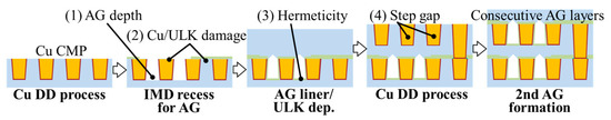
Figure 2.
Conventional AG process flow.
This AG process has the following challenges: (1) AG depth targeting without line collapse; (2) Cu damage during the IMD recess, which results in resistance degradation, and ultra-low-k (ULK) damage during plasma treatment of the AG process in the non-gapped area, which causes capacitance degradation and defect generation; (3) the thin AG liner which prohibits moisture uptake; and (4) the step gap at the next level, which causes insufficient Cu node separation. We describe our approaches to overcome these challenges in Section 4.
2.3. Design Restrictions
The practical use of the AG requires a definition of the key design rules to avoid process risks. First, the AG is allowed only at the minimum spacing [11,12]. Because of the self-aligned AG process, the IMD recess width for the AG increases with the spacing width. Then, the pinch-off point to close the AG becomes higher, resulting in the risk of contact with the trench bottom of the upper metal level. Second, the AG is prohibited beside the upper via [11,12,13,14]. If a part of the via bottom is outside of the metal line because of size and overlay variation, the via hole is connected to the AG cavity. Thus, the AG can be placed in the minimum spacing, which is at least one pitch away from the upper via.
There are other rules for confining the AG strictly between the minimum-pitch metal lines to obtain the expected pinch-off feature. Two sides of the AG open mask should be on the Cu line for realizing the self-aligned patterning. Additionally, the AG cannot be built at the end of the routing metal pattern.
3. AG-aware Design Methodology
3.1. Performance Investigation
One of the key ideas of our proposed design methodology is to route timing-critical nets on the optimal metal layers for the AG. In this section, we define the performance gain and then identify the optimal set of metal layers for the AG via an analytical method. The performance gain due to the AG depends on the maximum possible usage of the AG on each metal layer, which is limited by the specific AG design rules. However, routing on the metal layers with the highest probability of AG presence is not the ideal solution, because the wire resistance–capacitance (RC) can increase. Hence, to identify the optimal layers for the AG, the RC changes for the selected combination of layers should be considered together with the capacitance reduction due to the AG. Table 1 presents the notation for our formulations.

Table 1.
Description of notations.
For a given RC network, the propagation delay for a single stage of buffered interconnects is defined by Equation (1), which is derived from the Elmore equation [21].
The total performance gain is defined in Equation (2) by the performance gain from parasitic RC changes due to the AG-aware routing optimization, as well as the performance gain due to the capacitance reduction caused by the AG.
Using Equations (1) and (2), we can derive and , as given by Equations (3) and (4), with delay portions of the driving date and interconnect , excluding the from Equation (1).
To calculate the performance gain in Equations (2)–(4), we used a : ratio of 7:3 and a :: ratio of 3:6:1. These are the average values extracted from 300,000 gate stages on the critical paths among the 5,431,746 gate stages in the CPU10-A. Figure 3 compares the performance gains for 49 combinations of routing metal layers, i.e., all the available options for the AG. According to our analysis, the eighth option (8_M5_6), which consisted of the 5th and 6th metal layers, yields the best performance gain, as highlighted in Figure 3. The performance gain increases with the use of higher-level metal layers, i.e., p80, because of the smaller resistance resulting from the larger width, as well as the higher AG portion resulting from the longer interconnect. The 8th option exhibited better performance than the 9th option (9_M6_7), which has a higher chance of AG placement owing to the higher metal layers. This is because the gain improvement due to the resistance reduction resulting from the lower-via usage surpasses the gain reduction due to the lower AG portion. The 6th option (6_M4_5) exhibited lower performance than the 8th option despite the lower via usage, because M4 was the lowest among the p80 layers and had a larger sheet resistance than the other p80 layers owing to the thinner metal.
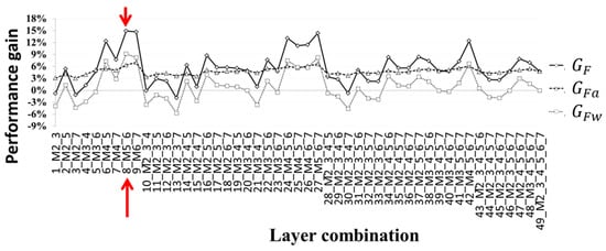
Figure 3.
AG performance gain results estimated by the analytical method.
3.2. AG-Aware Routing Method
We give higher priority to the timing-critical nets to be routed on the selected AG-applied layers—the 5th and 6th metal layers—which were identified as the best options in Section 3.1. Figure 4b depicts the routing structure of the timing-critical nets in the timing-critical region in Figure 4c, and Figure 4a shows the nets outside after routing. We then apply AG to the 5th and 6th metal layers to maximize the performance gain of the timing-critical paths. Figure 5 shows the implementation flow with the proposed two-step routing approach.
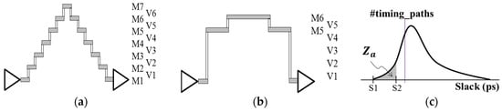
Figure 4.
Routing structures for (a) typical nets on all metal layers and (b) timing-critical nets on the optimal AG layers. (c) Critical-path zone, , on the slack distribution graph for applying AG-aware routing.
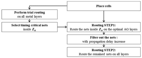
Figure 5.
AG-aware implementation flow with two-step routing.
4. Overcoming Process Challenges
4.1. AG Depth Control
The most critical process challenge is controlling the IMD recess to ensure the AG depth without metal collapse, as shown in Figure 6a. A highly selective dry-etching process to minimize the Cu attack suffers from etch stoppage at some point, and it is difficult to recess deeply enough to obtain the target. Therefore, a wet recess step follows the dry recess to compensate for the insufficient depth, as shown in Figure 6b. This is called “hybrid recess.” An additional HF strip between the dry recess and removes the high-density layer at the bottom of the ULK, which prevents penetration. This process achieves a controllable recess depth through adjustment of the time, as shown in Figure 6c.
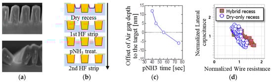
Figure 6.
(a) Cross-sections of shallow and excessively deep AGs. (b) Process flow. (c) AG depth with respect to the time in the hybrid recess scheme. (d) Lateral capacitance vs. wire resistance of the AG wire with intermetal dielectric (IMD) recess schemes.
However, because of the defect generation during the multiple process steps of the hybrid recess, and higher costs, we introduced a dry-only recess process without the etch-stoppage feature, using new etch chemistry. The developed dry-only recess achieves a comparable capacitance to the hybrid recess without a resistance penalty, as shown in Figure 6d.
4.2. Cu/ULK Damage
Because Cu is exposed during the IMD recess process, the Cu surface suffers physical and chemical damage, as shown in Figure 7a. Therefore, the AG process should adopt a protection layer on the Cu surface—a selective Co capping—during the IMD recess [11,12]. However, selective Co deposition includes an intrinsic plasma process, which damages the ULK surface. The damaged ULK surface is a C-depleted oxide-like layer and dissolves in the HF strip. To avoid this issue, we developed a silylation treatment to supply C for the recovery of the damaged layer. Figure 7c shows the wire resistance after the AG process with respect to the CoSi thickness. A large resistance at the thin CoSi indicates Cu damage, and a thicker CoSi (>3 nm) sufficiently protects the Cu surface. The physical observation in Figure 7b proves the effect of the Cu protection.
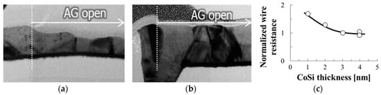
Figure 7.
Cross-sections of (a) unprotected Cu and (b) Cu protected with CoSi (c) wire resistance of the 40 nm-wide wire in the AG region with respect to the CoSi thickness.
4.3. Hermetic AG Liner
Insufficient coverage of the AG liner causes moisture uptake into the IMD, degrading the TDDB lifetime [22]. Furthermore, the AG liner at the top and sidewall affects the effective elastic modulus of the metal lines, which is nearly proportional to the EM lifetime [23]. Although a thicker AG liner is better for reliability, there is a tradeoff with the capacitance gain, because the liner consumes the AG portion. We introduce a pulsed-plasma chemical vapor deposition (CVD) process. Pulsed plasma keeps radicals rather than ions, as illustrated in Figure 8a, and the pulse frequency can be adjusted to control the step coverage in the range of 30.0–100.0%. Thus, optimization of the pulsed-plasma CVD yielded a hermetic liner with 5 nm step coverage, as shown in Figure 8b. The optimized thin hermetic liner maintained a stable capacitance even after 7 d in an air atmosphere, whereas a non-optimized liner exhibited capacitance degradation with a wide spread because of the degree of moisture uptake, as shown in Figure 8c.
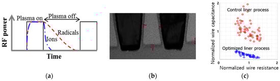
Figure 8.
AG liner optimization. (a) Process of pulsed-plasma chemical vapor deposition (CVD). (b) TEM image showing the sidewall and bottom coverage of the optimized liner process. (c) R–C plots for different liner processes.
4.4. Step-Height Control Above AG
The HM for AG patterning causes a geometrical height difference between the AG and non-AG areas. The step gap causes Cu residue after CMP of the next metal level, resulting in a leakage issue. We minimized the permanent HM thickness by combining it with a thicker sacrificial SiN HM. Figure 9 shows the process flow of this concept and leakage data for the metal lines above the AG. Replacing the thick permanent SiCN HM with thin SiCN/thick sacrificial SiN completely fixed the leakage issue.
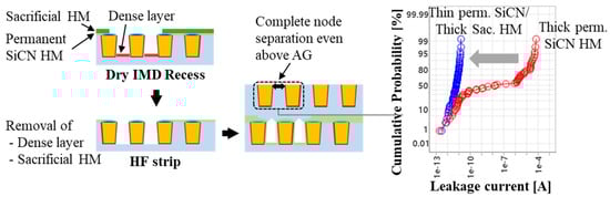
Figure 9.
Leakage current of the minimum-pitched metal layer above AG for different HM schemes, and process flow of a sacrificial HM scheme.
5. Experimental Results.
5.1. Capacitance Gain, Logic Yield, and Reliability
Figure 10a shows cross-sectional images of consecutive AG layers. We achieved a 17.0% capacitance reduction without a resistance penalty, as expected from the simulation of the assumed structure, as shown in Figure 10b.
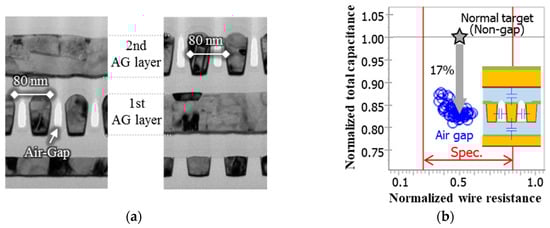
Figure 10.
(a) Cross-sectional TEM images of consecutive AG layers and (b) RC plot of p80 wires with AG.
Figure 11 shows the test results for the TDDB/EM reliability with the AG structure on p80. In a normal damascene structure without an AG, TDDB failure occurs at the interface between the dielectric barrier SiCN and the IMD. However, in the AG structure, the SiCN liner covered the top and side of metal lines, and the path length of the SiCN interface was longer than that in the normal damascene. This led to superb TDDB performance for the AG, as shown in Figure 11a. Figure 11b shows that the EM in the AG case was degraded compared with that in the non-AG case. However, the EM lifetime of the AG case satisfied the 10-year criteria. Figure 11c shows the yield of the logic blocks for five wafers, normalized with respect to the non-AG wafers. This plot includes the yield of a CPU block with 2.3 million instances and a CAM block with 3.2 million instances. The normalized logic yield of both blocks with the AG was comparable to that of non-AG wafers, implying that the optimized AG process generated no systematic defects in the complicated and practical logic wire patterns.
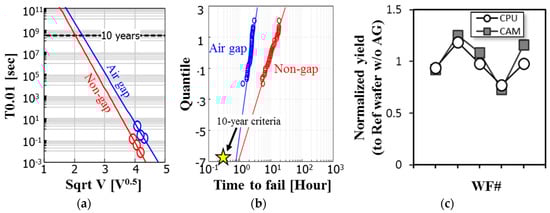
Figure 11.
Results of the reliability test with and without the AG for the (a) TDDB and (b) EM. (c) Yields of logic blocks with AG, normalized with respect to those of non-AG wafers.
5.2. Performance Gain
Table 2 presents the performance improvement achieved by our proposed timing criticality-aware AG design methodology for the CPU10-A (Figure 12b). We applied the best AG metal combination option, which was identified in Section 3. Figure 12a compares the slack distributions of conventional routing and two-step routing before and after application of the AG. With only the capacitance reduction from the AG, we observed a 6.1% improvement. With the routing optimization, improvements of 8.4% and 0.4% in the total power saving were achieved compared with the conventional AG design methodology.
Table 2.
Performance comparison on the CPU10-A.
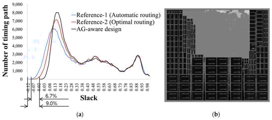
Figure 12.
CPU10-A design: (a) slack distribution of the proposed AG-aware design and references and (b) chip layout.
We also verified the routing quality. Our proposed design methodology resulted in similar or even better route-ability than the conventional methodology: (1) the portion of critical-path nets inside to be routed using AG-applied metal layers in the 1st routing step satisfied the criteria, and (2) the total wire length for all the metal layers was reduced by 1.4%. Regarding the AG-related routing quality of results (QoR), the length of the critical nets decreased by 5.0%, the usage of the AG-applied layers of the critical nets increased to 93.9%, and the AG portion per net increased to 51.7%. The improved QoR metrics prove the superior route-ability of the proposed methodology.
6. Conclusions
We developed an analytical method to identify the optimal metal layers for applying an AG. According to our formulations and analyses, we found that the ideal AG options depend on the metal level, via count, and available AG portions, and we concluded that intermediate-level layers, i.e., M5 and M6, were the best options for the AG. We then proposed an AG-aware design methodology with a two-step routing approach based on timing criticality. The proposed design methodology achieved a performance gain of 6.1–8.4% compared with the traditional AG design methodologies, without sacrificing area or power.
We developed an AG process to perform Si validation by overcoming the process challenges, such as the AG depth control, Cu/ULK damage, hermetic AG liner, and step-height control above the AG. We achieved a capacitance reduction of 17.0% while maintaining the target resistance. The logic yield of the AG wafers was comparable to that in non-AG wafers, indicating that it was free of defects. Applying the AG improved the TDDB lifetime, and the EM lifetime satisfied the 10-year criteria.
Author Contributions
Conceptualization, S.R. and Y.C.; methodology, S.R.; software, S.R.; validation, S.R. and Y.C.; formal analysis, S.R. and Y.C.; investigation, S.R. and Y.C.; resources, S.R. and Y.C.; data curation, S.R. and Y.C.; writing—original draft preparation, S.R; writing—review and editing, T.H.H.; visualization, S.R.; supervision, T.H.H.; project administration, T.H.H.; funding acquisition, T.H.H.
Funding
This work was supported by Samsung Electronics.
Conflicts of Interest
The authors declare no conflict of interest.
References
- Hayashi, Y. Impacts of low-k film on sub-100 nm-node, ULSI devices. In Proceedings of the IEEE 2002 International Interconnect Technology Conference (Cat. No. 02EX519), Burlingame, CA, USA, 5 June 2002; pp. 145–147. [Google Scholar]
- Tada, M.; Inoue, N.; Hayashi, Y. Performance Modeling of Low-k/Cu Interconnects for 32-nm-Node and Beyond. IEEE Trans. Electron Devices 2009, 56, 1852–1861. [Google Scholar] [CrossRef]
- Inoue, N.; Tagami, M.; Itoh, F.; Yamamoto, H.; Takeuchi, T.; Saito, S.; Furutake, N.; Ueki, M.; Tada, M.; Suzuki, T. 45nm-node interconnects with porous SiOCH-stacks, tolerant of low-cost packaging applications. In Proceedings of the 2007 IEEE International Interconnect Technology Conference, Burlingame, CA, USA, 3–6 June 2007; pp. 181–183. [Google Scholar]
- Watanabe, T.; Hayashi, Y.; Tomizawa, H.; Usui, T.; Gawase, A.; Shimada, M.; Watanabe, K.; Shibata, H. Robust BEOL Process Integration with Ultra Low-k (k = 2.0) Dielectric and Self-Formed MnOx Barrier Technology for 32 nm-node and beyond. In Proceedings of the 2008 International Interconnect Technology Conference, Burlingame, CA, USA, 1–4 June 2008; pp. 208–210. [Google Scholar]
- Liu, H.; Widodo, J.; Liew, S.; Wang, Z.; Wang, Y.; Lin, B.; Wu, L.; Seet, C.; Lu, W.; Low, C. Challenges of ultra low-k integration in BEOL interconnect for 45nm and beyond. In Proceedings of the 2009 IEEE International Interconnect Technology Conference, Sapporo, Japan, 1–3 June 2009; pp. 258–260. [Google Scholar]
- Kohl, P.A.; Bhusari, D.M.; Wedlake, M.; Case, C.; Klemens, F.P.; Miner, J.; Lee, B.-C.; Gutmann, R.J.; Shick, R. Air-gaps in 0.3 μm electrical interconnections. IEEE Electron Device Lett. 2000, 21, 557–559. [Google Scholar] [CrossRef]
- Gosset, L.; Gaillard, F.; Bouchu, D.; Gras, R.; De Pontcharra, J.; Orain, S.; Cueto, O.; Lyan, P.; Louveau, O.; Passemard, G. Multi-level Cu interconnects integration and characterization with air gap as ultra-low K material formed using a hybrid sacrificial oxide/polymer stack. In Proceedings of the 2007 IEEE International Interconnect Technology Conference, Burlingame, CA, USA, 3–6 June 2007; pp. 58–60. [Google Scholar]
- Daamen, R.; Bancken, P.; Badaroglu, D.E.; Michelon, J.; Nguyen, V.; Verheijden, G.; Humbert, A.; Waeterloos, J.; Yang, A.; Cheng, J. Multi-level air gap integration for 32/22nm nodes using a spin-on thermal degradable polymer and a SiOC CVD hard mask. In Proceedings of the 2007 IEEE International Interconnect Technology Conference, Burlingame, CA, USA, 3–6 June 2007; pp. 61–63. [Google Scholar]
- Nakamura, N.; Matsunaga, N.; Kaminatsui, T.; Watanabe, K.; Shibata, H. Cost-effective air-gap interconnects by all-in-one post-removing process. In Proceedings of the IEEE 2008 International Interconnect Technology Conference, Burlingame, CA, USA, 1–4 June 2008; pp. 193–195. [Google Scholar]
- Gras, R.; Gaillard, F.; Bouchu, D.; Farcy, A.; Petitprez, E.; Icard, B.; Le-Denmat, J.; Pain, L.; Bustos, J.; Haumesser, P. 300 mm multi level air gap integration for edge interconnect technologies and specific high performance applications. In Proceedings of the IEEE 2008 International Interconnect Technology Conference, Burlingame, CA, USA, 1–4 June 2008; pp. 196–198. [Google Scholar]
- Harada, T.; Takahashi, M.; Murakami, K.; Korogi, H.; Sasaki, T.; Hattori, T.; Ogawa, S.; Ueda, T. Manufacturable low keff (keff <2.5) Cu interconnects by selective/low damage air gap formation. In Proceedings of the IEEE 2006 International Interconnect Technology Conference, Burlingame, CA, USA, 5–7 June 2006; pp. 15–18. [Google Scholar]
- Harada, T.; Ueki, A.; Tomita, K.; Hashimoto, K.; Shibata, J.; Okamura, H.; Yoshikawa, K.; Iseki, T.; Higashi, M.; Maejima, S. Extremely low Keff (1.9) Cu interconnects with air gap formed using SiOC. In Proceedings of the 2007 IEEE International Interconnect Technology Conference, Burlingame, CA, USA, 3–6 June 2007; pp. 141–143. [Google Scholar]
- Noguchi, J.; Oshima, T.; Matsumoto, T.; Uno, S.; Sato, K. Multilevel interconnect with air-gap structure for next-generation interconnections. IEEE Trans. Electron Devices 2009, 56, 2675–2682. [Google Scholar] [CrossRef]
- Yoo, H.; Balakrishnan, S.; Bielefeld, J.; Harmes, M.; Hiramatsu, H.; King, S.; Kobrinsky, M.; Krist, B.; Reese, P.; RamachandraRao, V. Demonstration of a reliable high-performance and yielding Air gap interconnect process. In Proceedings of the 2010 IEEE International Interconnect Technology Conference, Burlingame, CA, USA, 6–7 June 2010; pp. 1–3. [Google Scholar]
- Fischer, K.; Agostinelli, M.; Allen, C.; Bahr, D.; Bost, M.; Charvat, P.; Chikarmane, V.; Fu, Q.; Ganpule, C.; Haran, M. Low-k interconnect stack with multi-layer air gap and tri-metal-insulator-metal capacitors for 14nm high volume manufacturing. In Proceedings of the 2015 IEEE International Interconnect Technology Conference and 2015 IEEE Materials for Advanced Metallization Conference (IITC/MAM), Grenoble, France, 18–21 May 2015; pp. 5–8. [Google Scholar]
- Cong, J.J.; Leung, K.-S. Optimal wiresizing under Elmore delay model. IEEE Trans. Computer-Aided Des. Integr. Circuits Syst. 1995, 14, 321–336. [Google Scholar] [CrossRef]
- Pullela, S.; Menezes, N.; Pillage, L.T. Reliable non-zero skew clock trees using wire width optimization. In Proceedings of the 30th ACM/IEEE Design Automation Conference, Dallas, TX, USA, 14–18 June 1993; pp. 165–170. [Google Scholar]
- Tan, S.X.-D.; Shi, C.-J.R.; Lee, J.-C. Reliability-constrained area optimization of VLSI power/ground networks via sequence of linear programmings. IEEE Trans. Computer-Aided Des. Integr. Circuits Syst. 2003, 22, 1678–1684. [Google Scholar] [CrossRef]
- Chen, C.-P.; Chu, C.C.; Wong, D. Fast and exact simultaneous gate and wire sizing by Lagrangian relaxation. IEEE Trans. Computer-Aided Des. Integr. Circuits Syst. 1999, 18, 1014–1025. [Google Scholar] [CrossRef]
- Sapatnekar, S.S. Wire sizing as a convex optimization problem: exploring the area-delay tradeoff. IEEE Trans. Comput. -Aided Des. Integr. Circuits Syst. 1996, 15, 1001–1011. [Google Scholar] [CrossRef]
- Rabaey, J.M.; Chandrakasan, A.P.; Nikolic, B. Digital Integrated Circuits; Prentice Hall: Upper Saddle River, NJ, USA, 2002; Volume 2. [Google Scholar]
- Michelon, J.; Hoofman, R.J. Moisture influence on porous low-k reliability. IEEE Trans. Device Mater. Reliab. 2006, 6, 169–174. [Google Scholar] [CrossRef]
- Lee, K.-D.; Ogawa, E.T.; Yoon, S.; Lu, X.; Ho, P.S. Electromigration threshold for Cu/low k interconnects. In Proceedings of the IEEE 2003 International Interconnect Technology Conference (Cat. No. 03TH8695), Burlingame, CA, USA, 4 June 2003; pp. 259–261. [Google Scholar]


© 2019 by the authors. Licensee MDPI, Basel, Switzerland. This article is an open access article distributed under the terms and conditions of the Creative Commons Attribution (CC BY) license (http://creativecommons.org/licenses/by/4.0/).