Article

A New Rail-to-Rail Second Generation Voltage Conveyor

Department of Industrial and Information Engineering and Economics, University of L’Aquila, 67100 L’Aquila, Italy
*
Author to whom correspondence should be addressed.
Electronics 2019, 8(11), 1292; https://doi.org/10.3390/electronics8111292
Submission received: 2 October 2019 / Revised: 27 October 2019 / Accepted: 4 November 2019 / Published: 5 November 2019
(This article belongs to the Section Microelectronics)

Abstract

:
In this paper, a novel low voltage low power CMOS second generation voltage conveyor (VCII) with an improved voltage range at both the X and Z terminals is presented. The proposed VCII is formed by a current buffer based on a class AB regulated common-gate stage and a modified rail-to-rail voltage buffer. Spice simulation results using LFoundry 0.15 μm low-Vth CMOS technology with a ±0.9 V supply voltage are provided to demonstrate the validity of the designed circuit. Thanks to the class AB behavior, from a bias current of 10 µA, the proposed VCII is capable of driving 0.5 mA on the X terminal, with a total power consumption of 120 µW. The allowed voltage swing on the Z terminal is at least equal to ±0.83 V, while on the X terminals it is ±0.72 V. Both DC and AC voltage and current gains are provided, and time domain simulations, where the voltage conveyor is used as a transimpedance amplifier (TIA), are also presented. A final table that summarizes the main features of the circuit, comparing them with the literature, is also given.

1. Introduction

Since the introduction of current conveyors in 1968 [1], the well-known operational amplifiers (Op-Amps) have started to be replaced in several applications [2,3,4]. Generally, current conveyors take inherent advantages of current mode signal processing and, in comparison to conventional Op-Amp based circuits, those employing current conveyors exhibit better frequency performance and simpler circuitry [5,6]. A literature survey shows that, in current conveyor families, second generation current conveyors (CCIIs) [7,8,9,10,11,12] are the most widely used. However, as the CCII lacks a low impedance voltage output port, it is not suitable for applications requiring output signal in the voltage form because, in these cases, an extra voltage buffer is needed to provide low output impedance, which results in higher power consumption and higher chip area.
In [13], the idea of voltage conveyors (VCs) as the dual circuit of the current conveyors (CCs) was introduced. Based on this concept, the dual circuits of CCIIs have been called second generation voltage conveyors (VCIIs). In particular, VCIIs show a low impedance voltage output port. This feature makes VCIIs a highly suitable candidate to replace CCIIs in applications requiring voltage output because they alleviate the need for an extra voltage buffer. Recently, VCIIs have attracted the attention of researchers, and their applications in implementing filters, gyrators, oscillators, inverting and non-inverting voltage amplifiers, current to voltage converters, differentiators and integrators, and readout circuits have been reported [13,14,15,16,17,18,19,20].
The low voltage low power restrictions imposed by advanced technologies necessitate the design of a high performance VCII circuit that is able to operate under low supply voltages and to provide an appropriate voltage swing at the voltage output port. Since previous implementations of VCIIs have suffered from limited voltage swing at the voltage output port [14,15,16], in this paper, we propose a new low voltage low power VCII with improved voltage range (rail-to-rail, (RtR)) characteristic at the output of terminal Z, but also at the input of terminal X. This will fully take advantage of its inherent transimpedance amplifier (TIA) behavior, making it suitable in applications where information has to be converted from the current to the voltage domain [21,22]. The proposed VCII has been developed with low-Vth CMOS technology (LFoundry 0.15 µm), with a supply voltage of ±0.9 V, showing a voltage swing at least equal to 80% of the supply voltage range. The manuscript is organized as follows: Section 2 gives a short overview on the highlights of second generation voltage conveyors; Section 3 shows and analyzes the proposed rail-to-rail VCII; Section 4 shows the simulation results of the proposed circuit, together with a table that compares them to some other relevant works available in the literature. Finally, Section 5 draws conclusions.

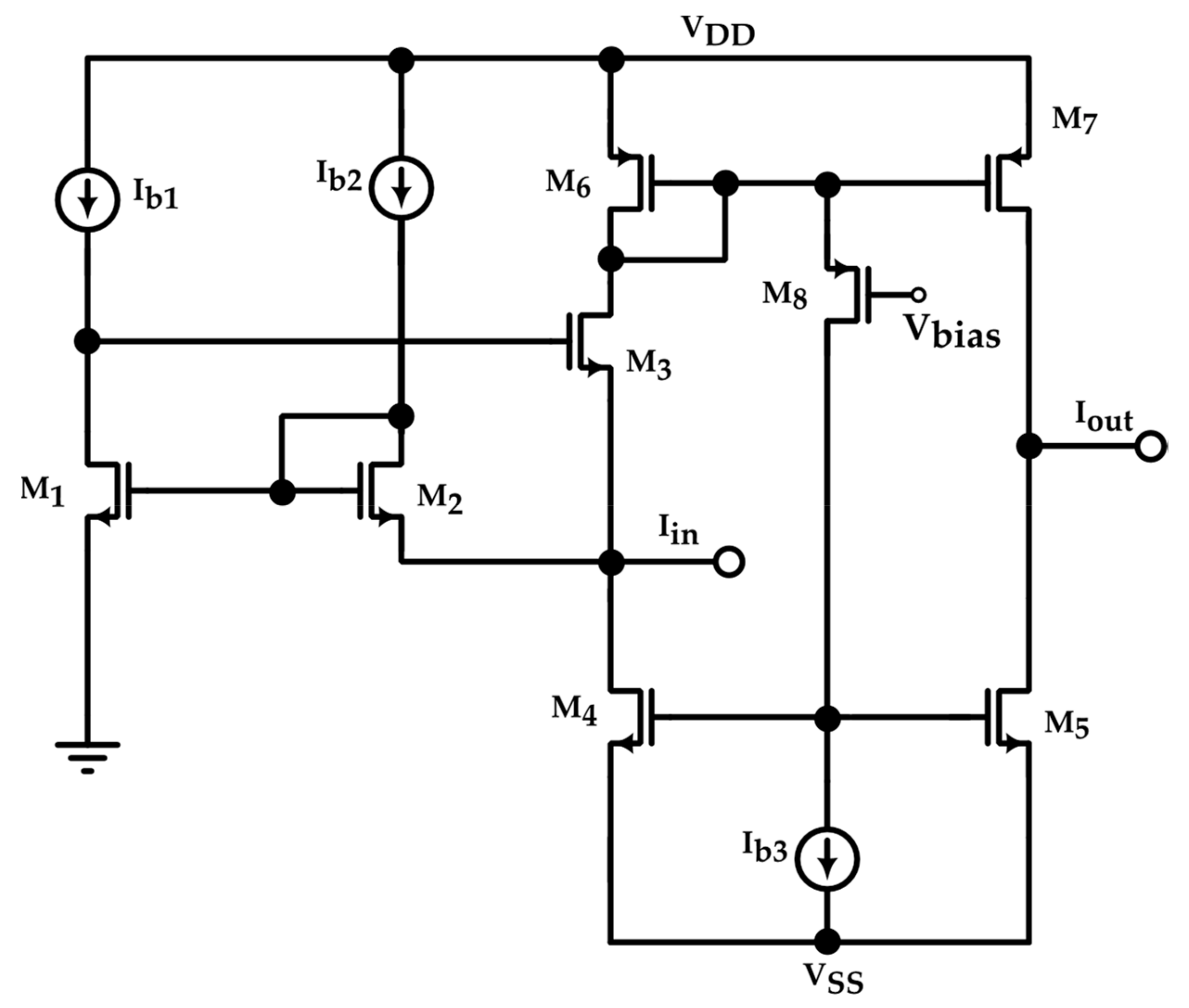
2. VCII Short Review

Figure 1 shows the internal structure (a) and symbol (b) of the second-generation voltage conveyor (VCII) as a dual circuit of the second-generation current conveyor (CCII). It consists of a current buffer between the Y and X terminals and a voltage buffer between the X and Z terminals. Unlike the CCII, the Y terminal of the VCII is a low impedance current input port with an ideal value of zero, X is a high impedance current output port with an ideal value of infinite, and Z is a low impedance voltage output port with an ideal value of zero. The relationship between port voltages and currents are expressed as:
i x V z = ± β 0 0 α i y V x
where VCII+ and VCII- are identified by +β and −β, respectively (where β should be close to 1). Ideally, the value of α is unity. Since the Y terminal has an extremely low input impedance, it can be considered as a virtual ground node. The main features of VCII can be summarized in three key points. Firstly, unlike other active blocks, current summing operation can be easily performed at the current input low impedance Y port. Secondly, having a low impedance voltage output Z port allows the flawless employment of the VCII in a voltage mode workflow, giving the flexibility to easily perform current mode operations to the designer. Finally, positive and negative voltage gains are simply obtained by employing VCII+ and VCII-, respectively.

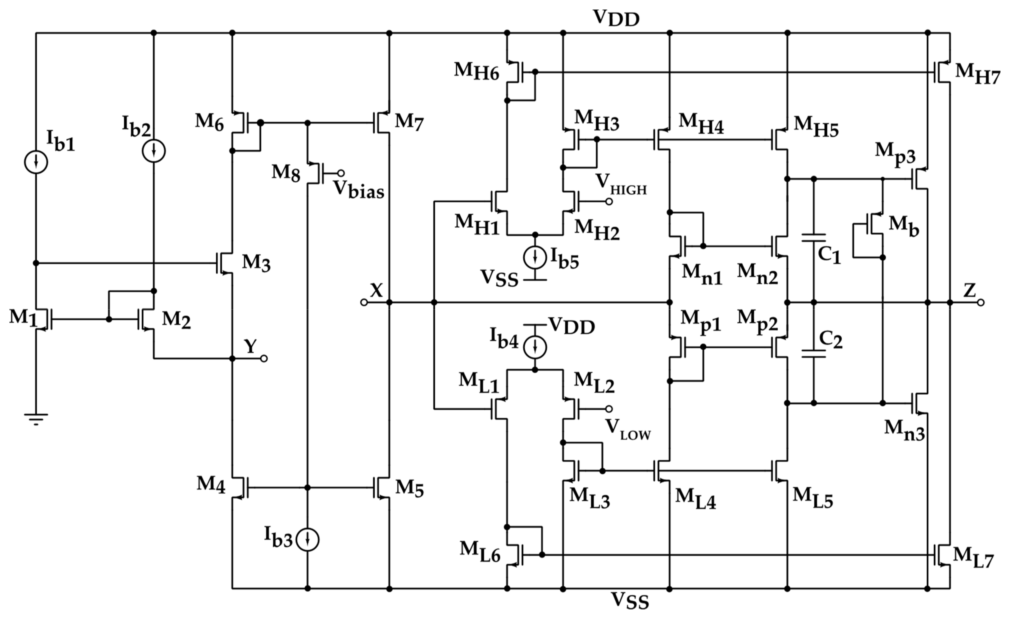
3. The Proposed RtR VCII

The proposed RtR-VCII is composed of a class AB current buffer between the Y and X terminals and an RtR modified voltage buffer between the X and Z terminals. Figure 2 shows the designed current buffer. It is formed by transistors M1M7 and the current sources Ib1–Ib3. Transistor M3 in the common-gate configuration is biased by a voltage that is regulated by the negative feedback loop established by M1M2, providing the virtual ground at the Y terminal and further reducing its impedance. The voltage buffer implementation is based on a modified version of the standard class AB voltage follower (see Figure 3a,b) [23]. PMOS ML1ML2 and NMOS MH1MH2 differential pairs drive a switching circuit that, based on the reference voltages VHIGH and VLOW, activate the correct portion of the buffer that is the standard voltage follower Mn1, Mn2, Mp1, Mp2, or the RtR pair MH7 and ML7. The working principle is explained in depth in [23].
The complete schematic of the proposed VCII is shown in Figure 4. M8 and Ib3 fix the voltage at the drain of M6. Then, it is possible to choose the gate voltage of M8 (Vbias) to accurately tune the bias current of the Y and therefore the X terminals. Capacitors C1 and C2 are used to dampen the α parameter transfer function, ensuring the stability of the system. The impedances are derived using the small signal equivalent model depicted in Figure 5. The impedance at the Y terminal is given by:
Z Y 1 g m M 3 g m M 1 r d s M 1 / / r o I B 1 .
Transistors M4M7 have the task of copying the input current (at Y) to the X terminal. Since the current flowing at Y is mirrored on the class AB-biased branch formed M5 and M7, the voltage swing allowed at the X terminal is very wid, even for high currents. Precisely, it is given by:
V s s + V d s M 5 V X V d d V s d M 7 .
The total input impedance at the X terminal can be approximated as follows:
Z X = R d s M 5 / / R d s M 7 .
Concerning the voltage output Z terminal, the allowed voltage swing can be evaluated as:
V s s + V d s , s a t M L 7 V Z V d d V s d , s a t M H 7 .
Since the output stage changes shape according to the voltage level at the X port, the output impedance can be evaluated as [23]:
Z Z R d s M n 3 R d s M p 3 R d s M n 3 + R d s M p 3 + R k 1 g m M p 3 R d s M p 3 + R k 2 g m M n 3 R d s M n 3   i f   V L O W < V X < V H I G H 1 g m M n 3 g m m p 2 R d s M p 2   i f   V X > V H I G H 1 g m M p 3 g m m n 2 R d s M n 2   i f   V X < V L O W
where Rk1 and Rk2 are equal to g m M n 2 R d s M n 2 R d s M p 3 / / R d s M H 5 and g m M p 2 R d s M p 2 R d s M n 3 / / R d s M L 5 , respectively.
The topology of the designed VCII allows it to be employed as a transimpedance amplifier. In fact, taking advantage of the high drive capability at X, together with the RtR behavior on X and Z, it is possible to achieve high gain conversion, even for large currents. A VCII used as a TIA is shown in Figure 6. The conversion gain can be easily set by a simple resistance value according to the following ideal equation:
V o u t V X = I Y R g a i n

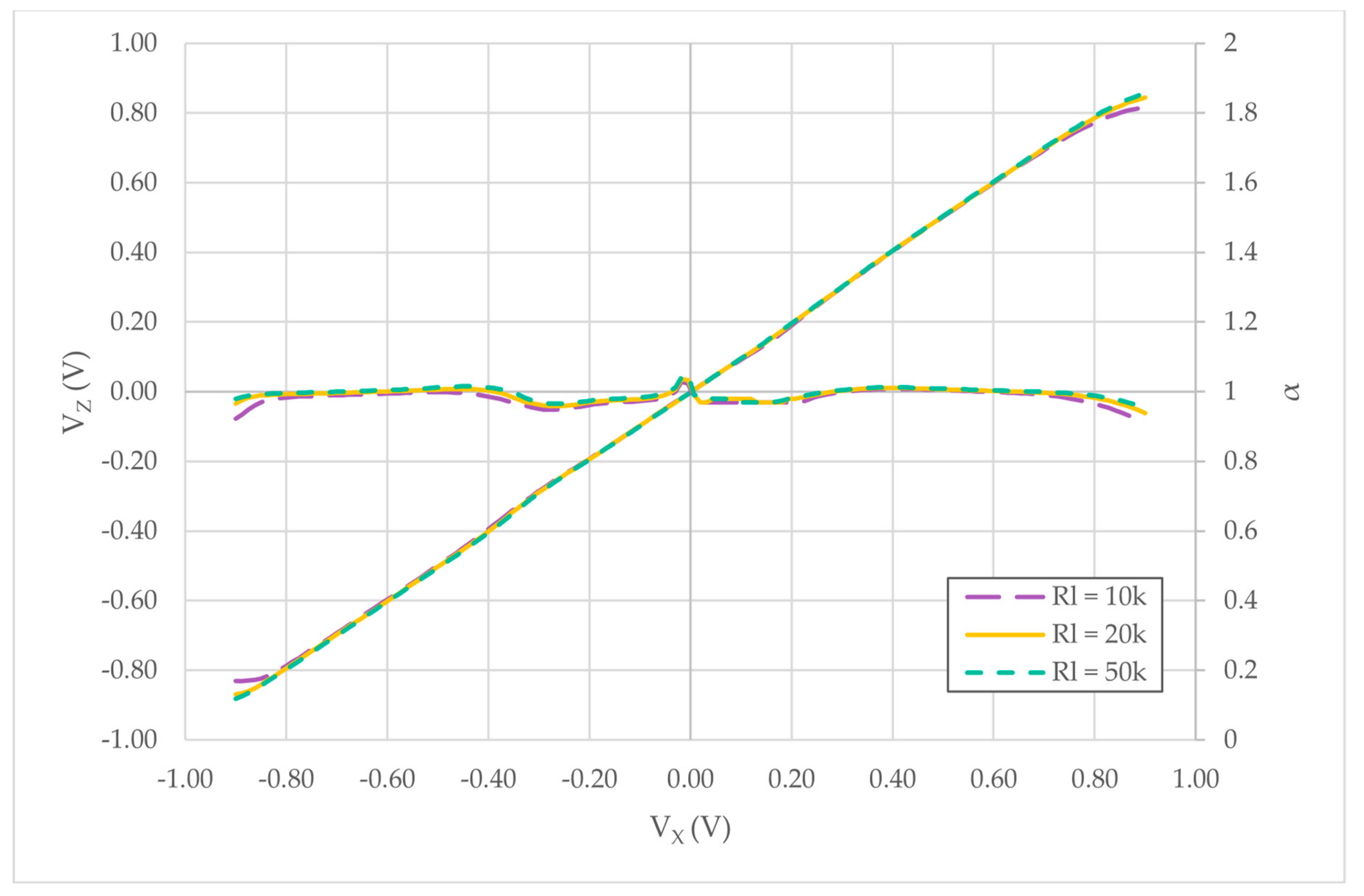
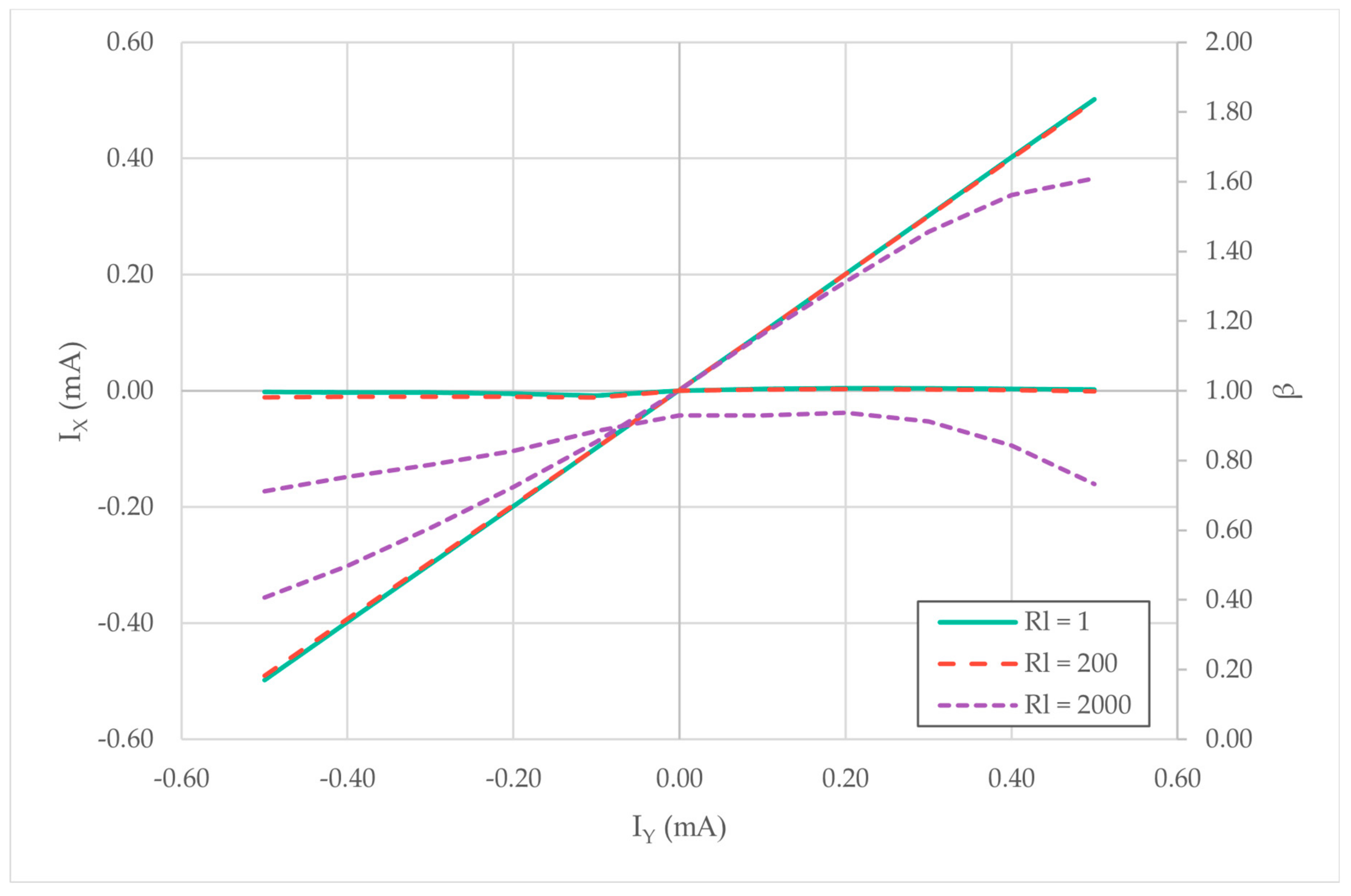
4. Simulation Results

Simulations were performed employing 0.15 µm CMOS technology from LFoundry through the Spice simulator. Current sources were implemented by means of simple current mirrors designed to provide a current of 5 µA. Transistor dimensions are shown in Table 1. For the proposed VCII, the two input voltages VHIGH and VLOW at the differential amplifiers of the voltage buffer stage were set to +0.3 V and −0.35 V, respectively, while supply voltages were ±0.9 V. The voltage Vbias was set to −0.3 V in order to ensure a 10 µA bias current through the Y and X branches. Mb dimensions were regulated so as to have 10 µA flowing through Mp3 and Mn3. In order to guarantee a high driving capability for the X node, the W/L ratio of M4M5 and M6M7 was set to 100 and 200, respectively.
The rail-to-rail capabilities of this circuit are shown in Figure 7 and Figure 8, where the DC performances of α and β are shown. To evaluate the former parameter, an input voltage at the X terminal, swinging from negative supply voltage to positive supply voltage, was applied, while the output voltage at the Z port was determined at different load levels (50 kΩ, 20 kΩ, 10 kΩ). As can be seen, α always remains greater than 0.95 for input voltages greater than ±0.8 V. Analogously, the performance of the β parameter was investigated by applying a current at the Y port and monitoring the current at the X port for different load levels. Figure 8 acknowledges both the good driving capability of currents of 0.5 mA (50 times greater than the X branch bias current) and the good voltage swing at X, which reaches ±0.72 V with a current of ±0.5 mA over a load of 2 kΩ.
Frequency performances of the voltage conveyor are presented in Figure 9 and Figure 10. The bandwidth for the α parameter, evaluated with a 1 pF load connected at the output Z node, was equal to 55 MHz (Figure 9). The β transfer function is shown in Figure 10. The bandwidth was equal to 165 MHz.
Terminal impedance values were also evaluated. The resulting values (see Figure 11) are 522 kΩ, 23 Ω, and 160 Ω at X, Y, and Z, respectively. To investigate the time domain behavior of the VCII, a 1 MHz sine wave with a 0.8 V peak amplitude was applied to the X terminal. The total harmonic distortion (THD) at the output (Z terminal) with a 1 pF, 10 kΩ parallel load, considering 10 harmonics, was equal to 2.4% (−32.4 dB). The same analysis was repeated, applying a 1 MHz sine wave with a 0.5 mA peak amplitude at the Y port. The X terminal was connected to a 100 Ω load. The THD was equal to 1.1% (−39 dB).
To show the benefit of the dual input-output rail-to-rail stages, the circuit was tested in a transimpedance amplifier configuration. A sinusoidal current on the input terminal Y, with an amplitude of 0.5 mV, was imposed and the output voltage at the X node was determined. The output was connected to a 1 pF capacitor in parallel to a 10 kΩ resistor. The gain resistor was set equal to 500 Ω and 1.5 kΩ to take advantage of the full X branch dynamic. Results are shown in Figure 12, acknowledging the capability of the circuit to reach a dynamic of 80% of the supply voltage without distortions.
Table 2 summarizes the circuit performance parameters, comparing them with other relevant manuscripts from the literature. The presented topology manages to achieve overall comparable performances with respect to the other circuits, while greatly improving the dynamic range of the voltage conveyor, as well as reducing its power consumption, as acknowledged by the figure of merit (FOM) (in this case, lower is better) parameter in the same table. In this regard, the parameter is calculated as [24]:
F O M = V D D + V S S V i n , p p _ m a x I µ A
where Vin,pp_max represents the maximum input peak-to-peak voltage that still allows it to achieve acceptable linearity levels and is extracted from the THD evaluations. The parameter, I, expressed in µA, introduces the FOM of the power consumption of the circuit, decoupling it from the actual supply voltage.
As can be seen from Table 2, the proposed topology links the current driving capabilities (at the Y terminal) of [16] to the extended input dynamic range (at the X and Z terminals). Moreover, unlike [17], where the authors make use of a universal voltage conveyor, the presented architecture uniquely implements a second generation voltage conveyor, thereby largely reducing the overall power consumption.

5. Conclusions

We have here presented a new CMOS VCII, showing RtR voltage swing at the X and Z ports. The dynamic biasing of the Y and X branches ensures a high driving capability at the X terminal with a low quiescent current. These two features, together, allow it to achieve high transimpedance conversion gains even for relatively large currents. Simulation results have been given, effectively acknowledging the predicted behavior. A possible application scenario has been proposed for a transimpedance amplifier configuration.

Author Contributions

Conceptualization, V.S., G.B., L.S. and G.F.; investigation, V.S., G.B. and E.D.; data curation, G.B., L.S. and E.D.; writing—original draft preparation, G.B., V.S. and G.F.; supervision, G.F. and V.S.

Funding

This research received no external funding.

Conflicts of Interest

The authors declare no conflict of interest.

References

  1. Smith, K.; Sedra, A. The current conveyor—A new circuit building block. Proc. IEEE 1968, 56, 1368–1369. [Google Scholar] [CrossRef]
  2. Grigorescu, L. Amplifier built with current conveyors. Rom. J. Phys. 2008, 53, 109–113. [Google Scholar]
  3. Mohan, P.; Papazoglou, C.; Karybakus, C. Comments on “A transformation to obtain CCII-based adjoint of op-amp based circuits” [with reply]. IEEE Trans. Circuits Syst. II Analog Digit. Signal Process. 2000, 47, 233. [Google Scholar] [CrossRef]
  4. Celma, S.; Martinez, P.; Sabadell, J. A transformation method for equivalent infinite-gain op amp to unity-gain CCII networks. IEEE Trans. Circuits Syst. I Fundam. Theory Appl. 1996, 43, 61–63. [Google Scholar] [CrossRef]
  5. Ferri, G.; Parente, F.; Stornelli, V.; Barile, G.; Pantoli, L. Automatic Bridge-based Interface for Differential Capacitive Full Sensing. Procedia Eng. 2016, 168, 1585–1588. [Google Scholar] [CrossRef]
  6. Hwang, H.; Lee, H.; Han, M.; Kim, H.; Chae, Y. A 1.8-V 6.9-mW 120-fps 50-Channel Capacitive Touch Readout with Current Conveyor AFE and Current-Driven Delta Sigma ADC. IEEE J. Solid-State Circuits 2018, 53, 204–218. [Google Scholar] [CrossRef]
  7. Palumbo, G.; Pennisi, S. A high-performance CMOS CCII. Int. J. Circuit Theory Appl. 2001, 29, 331–336. [Google Scholar] [CrossRef]
  8. Fabre, A.; Alami, M. A precise macromodel for second generation current conveyors. IEEE Trans. Circuits Syst. I Fundam. Theory Appl. 1997, 44, 639–642. [Google Scholar] [CrossRef]
  9. Stornelli, V.; Ferri, G.; Pantoli, L.; Barile, G.; Pennisi, S. A rail-to-rail constant-g m CCII for Instrumentation Amplifier applications. AEU-Int. J. Electron. Commun. 2018, 91, 103–109. [Google Scholar] [CrossRef]
  10. Bhargave, G.; Sheokand, P.; Kaur, J. A New Low Voltage and Low Power Filter Using DTMOS-CCII. In Proceedings of the 2015 IEEE Second International Conference on Advances in Computing and Communication Engineering, Dehradun, India, 1–2 May 2015; pp. 17–20. [Google Scholar] [CrossRef]
  11. Nunez, J.; Tlelo, E.; Ramirez, C.; Jimenez, J. CCII+ Based on QFGMOS for Implementing Chua s Chaotic Oscillator. IEEE Latin Am. Trans. 2015, 13, 2865–2870. [Google Scholar] [CrossRef]
  12. Svoboda, J. Current conveyors, operational amplifiers and nullors. IEE Proc. G Circuits Devices Syst. 1989, 136, 317. [Google Scholar] [CrossRef]
  13. Filanovsky, I. Current conveyor, voltage conveyor, gyrator. In Proceedings of the 44th IEEE 2001 Midwest Symposium on Circuits and Systems. MWSCAS 2001, Dayton, OH, USA, 14–17 August 2001; pp. 314–317. [Google Scholar] [CrossRef]
  14. Safari, L.; Barile, G.; Stornelli, V.; Ferri, G. An Overview on the Second Generation Voltage Conveyor: Features, Design and Applications. IEEE Trans. Circuits Syst. II Express Briefs 2019, 66, 547–551. [Google Scholar] [CrossRef]
  15. Barile, G.; Leoni, A.; Pantoli, L.; Safari, L.; Stornelli, V. A New VCII Based Low-Power Low-Voltage Front-end for Silicon Photomultipliers. In Proceedings of the 2018 3rd International Conference on Smart and Sustainable Technologies (SpliTech), Split, Croatia, 26–29 June 2018. [Google Scholar]
  16. Barile, G.; Ferri, G.; Safari, L.; Stornelli, V. A New High Drive Class-AB FVF Based Second Generation Voltage Conveyor. IEEE Trans. Circuits Syst. II: Express Briefs 2019. [Google Scholar] [CrossRef]
  17. Koton, J.; Herencsár, N.; Vrba, K. KHN-equivalent voltage-mode filters using universal voltage conveyors. AEU-Int. J. Electron. Commun. 2011, 65, 154–160. [Google Scholar] [CrossRef]
  18. Pantoli, L.; Barile, G.; Leoni, A.; Muttillo, M.; Stornelli, V. A Novel Electronic Interface for Micromachined Si-Based Photomultipliers. Micromachines 2018, 9, 507. [Google Scholar] [CrossRef] [PubMed]
  19. Čajka, J.; Vrba, K. The Voltage Conveyor May Have in Fact Found its Way into Circuit Theory. AEU-Int. J. Electron. Commun. 2004, 58, 244–248. [Google Scholar] [CrossRef]
  20. Safari, L.; Barile, G.; Ferri, G.; Stornelli, V. High performance voltage output filter realizations using second generation voltage conveyor. Int. J. RF Microw. Comput.-Aided Eng. 2018, 28, e21534. [Google Scholar] [CrossRef]
  21. Pantoli, L.; Muttillo, M.; Stornelli, L.; Ferri, G.; Gabriele, T. A Low Cost Flexible Power Line Communication System. Lect. Notes Electr. Eng. 2017, 413–420. [Google Scholar] [CrossRef]
  22. Orsetti, C.; Muttillo, M.; Parente, F.; Pantoli, L.; Stornelli, V.; Ferri, G. Reliable and Inexpensive Solar Irradiance Measurement System Design. Procedia Eng. 2016, 168, 1767–1770. [Google Scholar] [CrossRef]
  23. Wongfoo, S.; Naklo, W.; Suadet, A.; Kasemsuwan, V. A Simple Rail-to-Rail CMOS Voltage Follower. In Proceedings of the TENCON 2006–2006 IEEE Region 10 Conference, Hong Kong, China, 14–17 November 2006. [Google Scholar] [CrossRef]
  24. Balasubramanian, S.; Ismail, M. Rail-to-rail input stages: A voltage-mode design technique and a figure-of-merit. In Proceedings of the 8th IEEE International NEWCAS Conference 2010, Montreal, QC, Canada, 20–23 June 2010. [Google Scholar] [CrossRef]
  25. UVC-N1C 0520 Datasheet; ON Semi & Brno UoT. 2010. Available online: http://www.utko.feec.vutbr.cz/~herencsar/UVC_N1C_0520.pdf (accessed on 26 October 2019).
Figure 1. Second generation voltage conveyor (VCII): (a) Internal structure; (b) Symbol.
Electronics 08 01292 g001
Figure 2. The proposed class AB current buffer stage.
Electronics 08 01292 g002
Figure 3. (a) Simple voltage follower, (b) Modified rail-to-rail (RtR) voltage follower [23].
Electronics 08 01292 g003
Figure 4. The proposed VCII with Rail to Rail feature.
Electronics 08 01292 g004
Figure 5. Small signal equivalent model of the X and Y terminals.
Electronics 08 01292 g005
Figure 6. Transimpedance amplifier (TIA) implementation using a VCII+.
Electronics 08 01292 g006
Figure 7. DC performances of the α parameter at different load levels connected to the Z node.
Electronics 08 01292 g007
Figure 8. DC performances of the β parameter at different load levels connected to the X node.
Electronics 08 01292 g008
Figure 9. AC performances of the α parameter with a 1 pF capacitor connected to the Z node.
Electronics 08 01292 g009
Figure 10. AC performances of the β parameter.
Electronics 08 01292 g010
Figure 11. Proposed VCII terminal impedances.
Electronics 08 01292 g011
Figure 12. VCII used as a TIA.
Electronics 08 01292 g012
Table 1. Transistor dimensions and parameter values.
TransistorDimensions (W, L)
M1, M2, M81.8 µm, 0.3 µm
M32.4 µm, 0.3 µm
M4, M5, MH730 µm, 0.3 µm
M6, M7, ML760 µm, 0.3 µm
MH1, MH27.2 µm, 0.3 µm
MH3, MH4, MH5, MH63.6 µm, 0.3 µm
ML1, ML214.4 µm, 0.3 µm
ML3, ML4, ML5, ML62.85 µm, 0.9 µm
Mp1, Mp28.75 µm, 0.75 µm
Mn1, Mn22.85 µm, 0.75 µm
Mp34.5 µm, 0.75 µm
Mn31.35 µm, 0.75 µm
Mb0.3 µm, 0.6 µm
ParameterValue
Ib1, Ib2, Ib3, Ib4, Ib55 µA
VHIGH300 mV
VLOW−350 mV
Vbias−300 mV
C1, C2250 fF
Table 2. The Proposed VCII Performance Parameters.
ParameterThis Work[14][16][17,25][15,18]
TechnologyLFoundry 0.15 µmAMS 0.35 µmAMS 0.35 µmTSMC 0.35 µmAMS 0.35 µm
Supply voltage±0.9 V±1.65 V±1.65 V±1.65 V±1.65 V
Impedance at X node522 kΩ (@100 MHz)1.2 MΩ370 kΩ240 kΩ802 kΩ
Impedance at Y node23 Ω (@100 MHz)6.7 Ω2 mΩ650 mΩ49 mΩ
Impedance at Z node160 Ω (@100 MHz)0.7 Ω2 mΩ1.4 Ω79 mΩ
α−0.24 dB (@100 kHz)−0.03 dB−0.07 dB0.32 dB−0.04 dB
β−0.03 dB (@100 kHz)−0.1 dB−0.115 dB −0.04 dB
α bandwidth55 MHz (1 pF load at Z)217 MHz (unloaded)220 MHz (unloaded)74 MHz340 MHz (unloaded)
β bandwidth165 MHz200 MHz22.4 MHz64 MHz14 MHz
VZ THD2.4% (−32.4 dB) (VX = 1.6 Vpp; @1 MHz; 10 harm)0.068% (−63 dB) (VX = 1 Vpp; @1 MHz; 10 harm)2.48% (VX = 1 Vpp; @1 MHz; 10 harm)2.7% (VX = 1 Vpp)N.A.
IX THD1.1% (−39 dB) (IY = 1 mApp; @1 MHz; 10 harm)0.1% (−59 dB) (IY = 20 µApp; @1 MHz; 10 harm)3.36% (IY = 1 mApp; @1 MHz; 10 harm)N.A.N.A.
Static Power Cons.120 µW330 µW320 μW≅5 mW700 μW
figure of merit (FOM)853303204950874

