Article

Modeling, Design Procedure and Control of a Low-Cost High-Gain Multi-Input Step-Up Converter

by
Edgardo Netzahuatl
1,†,
Domingo Cortes
1,*,†,
Marco A. Ramirez-Salinas
2,‡,
Jorge Resa
1,‡,
Leobardo Hernandez
1,† and
Francisco-David Hernandez
1,†
1
Instituto Politecnico Nacional, ESIME Culhuacan, Mexico City 04440, Mexico
2
Instituto Politecnico Nacional, CIC, Mexico City 07738, Mexico
*
Author to whom correspondence should be addressed.
Avenida Santa Ana 951, Coyoacan, 04440, CDMX, Mexico.
Avenida Juan de Dios Batiz, Gustavo A. Madero, 07738, CDMX, Mexico.
Electronics 2019, 8(12), 1424; https://doi.org/10.3390/electronics8121424
Submission received: 7 November 2019 / Revised: 21 November 2019 / Accepted: 26 November 2019 / Published: 29 November 2019
(This article belongs to the Section Power Electronics)

Abstract

:
The use of several different sources to feed a load jointly is convenient in many applications, in particular those where two or more renewable energy sources are employed. These applications include energy harvesting, hybrid vehicles, and off-grid systems. A multi-input converter able to admit sources of different characteristics and select the output power of each source is necessary in such applications. Several topologies of multi-input converters have been proposed to this aim; however, most of them are controlled by simple strategies based on a small signal model of multi-input converters. In this work, a low cost high gain step-up multi-input converter is analyzed. A nonlinear model is derived. Using this model, a detailed design procedure is proposed. A 500 W converter prototype was constructed to confirm that the model predicted the real behavior of the converter. Using the nonlinear model, indirect voltage control of basic converters was extended to the multi-input converter. The obtained controller had a fast performance, and it was robust under load and input voltage variations. With the obtained model, the proposed design procedure, and the controller, a converter that was initially proposed for photovoltaic applications was enabled to be used in a broader range of applications. The herein exposed ideas for modeling, the design procedure, and control could be also applied to other multi-input converters.

1. Introduction

An intense research effort is being made to increase the use of renewable energy in all human activities. Techniques to take advantage of solar [1,2,3,4], wind [5,6,7], and hydrogen based [8,9,10], among other kinds of clean energies, are being developed. In some applications, it is necessary to jointly use several of these sources to feed a single load. If several sources collaborate to feed a load, it would be convenient to select the most adequate source at any given time (due to cost, availability, or other parameter) to feed a load. If a single source is not sufficient, a second source could be used; if both are not sufficient, a third can be used, and so on. For this to be possible, a multi-input converter is necessary [11]. In addition to regulating the load voltage and being robust under load variations, such a converter should accept sources with variable voltage and different voltages among them. Furthermore, this converter should be able to extract different energy portions from each source, and the energy that each source provides must be independent of its output voltage. Among the applications where this scheme is favorable are energy harvesting for wireless sensors [12,13,14], smart buildings [15,16], hybrid and electric cars [17,18,19,20,21,22,23], off-grid systems in rural areas [24,25,26], etc.
An adequate topology with a proper control is required to fulfill all these features. Aimed at constructing an appropriate converter for such applications, different composite topologies derived from classic buck and boost converters have been proposed [27,28,29,30,31,32]. It is known that multi-phase converters can reduce current stress by sharing the total power in each of the devices; however, it is also known that current imbalances may occur in these kinds of topologies [29,33,34]. Such imbalances are mainly caused by parasitic elements and duty cycle mismatch. Studies are still being conducted to control and compensate for this issue [34,35,36]. Some previously proposed topologies have limited output power [37,38,39] or impose an input voltage restriction among the sources [40,41,42], and others increase the number of components severely for each added source [32,40].
On the controller part, most published works are based on small signals, that is linear models of multi-input converters, and consequently, most proposed controllers are linear [43,44,45,46]. A nonlinear control scheme for a two input boost converter was presented in [47]; the controller prevents currents from entering discontinuous conduction mode (DCM). However, the conversion range is still limited by the topology itself.
Step-up multi-input converters are more problematic than step-down converters. They exhibit a non-minimum phase characteristic, and their topology tends to be more complicated, particularly for high gain step-up converters. Hence, designing a controller for these converters becomes more difficult [47]. In [48], a step-up multi-input converter with salient features was proposed: from the second source, each additional source increases the overall converter voltage gain; hence, it is a high gain converter for two or more sources; it admits a wide duty cycle range (0.5–1) without entering in DCM; there is no restriction on the voltage value that input sources may have, and only one pair of transistor-diode and only one capacitor are necessary for each added source.
Unfortunately, there is not a precise model nor a design procedure for this converter. The only controller that has been proposed is a PI controller designed for its linear approximation. It is known that the use of this controller in non-minimum phase systems yields a very slow response [49]. In this work, the low cost high gain step-up multi-input converter topology proposed in [48] is analyzed. Nonlinear switched and average models are obtained. Based on the equilibrium analysis and the switched model, a precise designing procedure is derived. A 500 W prototype is constructed to make sure that the model and design procedure predict what happens in reality and to evaluate the converter efficiency and reliability. The indirect control idea of controlling the output voltage through the control of the inductor current is revisited and extended to propose a control strategy for the multi-input converter. The controller obtained has a fast performance and is robust under load and input voltage variations. Furthermore, it admits sources with different voltages and can make each source provide a selectable portion of the total power delivered to the load.
The paper is organized as follows. In Section 2, the topology proposed in [48] is revisited. The nonlinear model of the converter is developed in Section 3. Based on equilibrium analysis and the nonlinear switched model, a design procedure is derived in Section 4. In Section 5, experimental results obtained using the constructed prototype are presented and analyzed. The proposed controller is derived in Section 6. Simulation results obtained with this controller are also presented in this section. Finally, some conclusions are given.

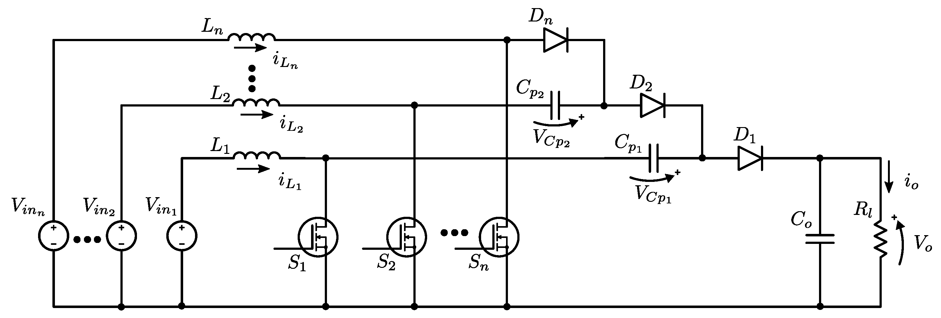
2. A Multi-Input High Gain Step-Up Converter

The converter analyzed in this paper is shown in Figure 1 and was first proposed in [48]. The converter can be seen as a source-inductor-switch cell connected to an RCnetwork to form a classic boost converter. Then, a second cell of the source-inductor-switch is connected to the RC network trough a buffer capacitor, forming a two input step-up converter. More of these second cells can be added to form a multi-input step-up converter.
Although in [48], a converter was proposed for photovoltaic applications, in this work, it is shown that with a proper control strategy, the converter can accept sources of different voltages, and each source can provide different amounts of current independent of its voltage. It is also shown that with an adequate control strategy, the converter can be robust to input voltage and load variations.
For the sake of simplicity, in what follows, the two input case is considered. However, once the two input case is understood, it is not difficult to extend the results to the general case. The special case of two inputs is shown in Figure 2. The PWM signals applied to the transistor are shifted a half of period from each other. Depending on the switches’ position, the converter has four operation modes shown in Figure 3. Note that Mode 1 and Mode 3 are the same. Capacitor C p is disconnected in these modes, thus during the time the converter is in any of these modes, voltage trough C p is held. The case where both transistors are off is avoided by restricting the duty cycle of both transistors to be larger than 0.5. One of the main advantages of this converter is the possibility to operate each transistor at different duty cycles without having one stage operating in continuous conduction mode and the other in discontinuous conduction mode, in contrast to the common interleaved boost converters [36]. From these operation modes, in the next section, a nonlinear model is obtained.

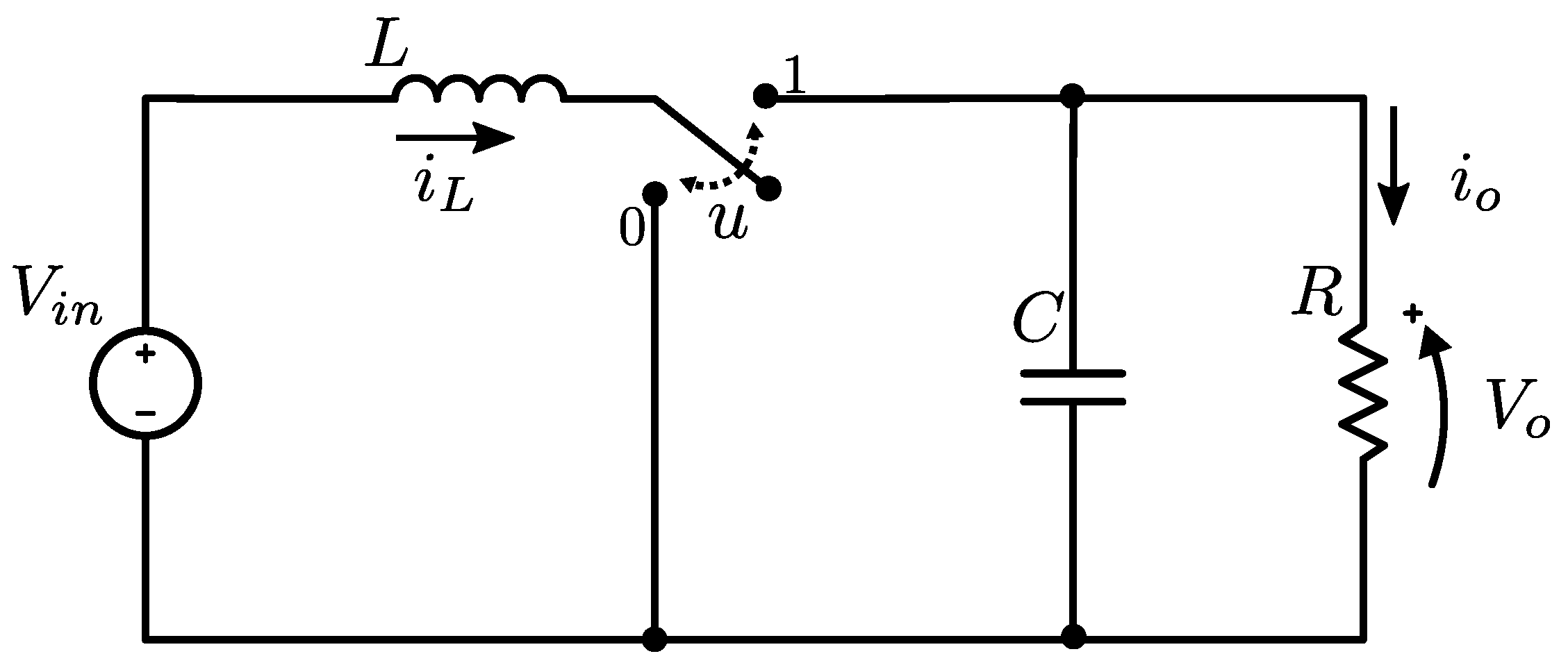
3. A Nonlinear Model for the Converter

The state-space standard notation is useful in the modeling and control of dynamical systems. For this reason, hereafter, electrical variables and state variables’ notation given by:
x 1 = i L 1
x 2 = i L 2
x 3 = V C p
x 4 = V C o = V o
are used interchangeably. Using the previous notation and applying Kirchhoff laws to every circuit depicted in Figure 3, the following models can be obtained:
  • Mode 1 and Mode 3: S 1 , S 2 = on:
    x ˙ 1 = V i n 1 L 1
    x ˙ 2 = V i n 2 L 2
    x ˙ 3 = 0
    x ˙ 4 = x 4 C o R l
  • Mode 2: S 1 = on, S 2 = off:
    x ˙ 1 = V i n 1 L 1
    x ˙ 2 = V i n 2 L 2 x 3 L 2
    x ˙ 3 = x 2 C p
    x ˙ 4 = x 4 C o R l
  • Mode 4: S 1 = off, S 2 = on:
    x ˙ 1 = V i n 1 L 1 + x 3 L 1 x 4 L 1
    x ˙ 2 = V i n 2 L 2
    x ˙ 3 = x 1 C p
    x ˙ 4 = x 1 C o x 4 C o R l
Introducing the notation:
u 1 = 1 if S 1 = o f f 0 if S 1 = o n
u 2 = 1 if S 2 = o f f 0 if S 2 = o n
Expressions (2)–(4) can be written in a single set of expressions as follows:
x ˙ 1 = V i n 1 L 1 + x 3 L 1 x 4 L 1 u 1
x ˙ 2 = V i n 2 L 2 x 3 L 2 u 2
x ˙ 3 = x 1 C p u 1 + x 2 C p u 2
x ˙ 4 = x 4 C o R l + x 1 C o u 1
The expressions (6) model the converter depicted in Figure 2. Variables u 1 and u 2 are regarded as the control inputs of this model. Note that these variables can only have two values because u 1 , u 2 { 0 , 1 } ; thus, Model (6) is a nonlinear switching model.
It has been shown in discontinuous differential equation theory [50] and by the heuristic approach [51] that if switching signals u 1 and u 2 change fast enough, an average model can be obtained. The average model results:
x ˜ ˙ 1 = V i n 1 L 1 + x ˜ 3 L 1 x ˜ 4 L 1 u ˜ 1
x ˜ ˙ 2 = V i n 2 L 2 x ˜ 3 L 2 u ˜ 2
x ˜ ˙ 3 = x ˜ 1 C p u ˜ 1 + x ˜ 2 C p u ˜ 2
x ˜ ˙ 4 = x ˜ 4 C o R l + x ˜ 1 C o u ˜ 1
where f ˜ means the average of f. Note that the average model looks very similar to the switching model; however, the meaning of the variables is different. Due to the definitions of u 1 and u 2 given by (5), the relations between transistors’ duty cycles d 1 , d 2 , and u ˜ 1 , u ˜ 2 are:
d 1 = 1 u ˜ 1
d 2 = 1 u ˜ 2
Useful information can be obtained from Models (6) and (7). From the average Model (7), the conditions for the existence of an equilibrium (stationary) state can be found. Switching Model (6), on the other hand, gives detailed information about what happens within a switching period. From this information, appropriate components’ values can be found to keep signals’ ripples lower than predefined values.
From Model (7), stationary values can be found. In the stationary state, the derivative of average signals is zero, that is x ˜ ˙ 1 = x ˜ ˙ 2 = x ˜ ˙ 3 = x ˜ ˙ 4 = 0 . Hence, equaling the right hand side of Expressions (7) to zero, the following is obtained:
x ¯ 3 = V i n 2 u ¯ 2
x ¯ 4 = V i n 1 u ¯ 1 + V i n 2 u ¯ 2
x ¯ 1 u ¯ 1 = x ¯ 4 R l
x ¯ 2 u ¯ 2 = x ¯ 4 R l
where f ¯ means the stationary value of f. Expression (9b) shows that the output voltage is equal to the sum of two voltages as if there were two independent boost converters. Hence, it is convenient to define the voltage gain for each source as:
M 1 = V ¯ o V i n 1 = x ¯ 4 V i n 1
M 2 = V ¯ o V i n 2 = x ¯ 4 V i n 2
Note that the output current is given by:
i o = x 4 R l
Thus, from Equations (9c), (9d) and (11):
x ¯ 1 u ¯ 1 = x ¯ 2 u ¯ 2 = i ¯ o
Expression (12) means different duty cycles yield different stationary inductor currents. To further make stationary current values precise, it is necessary to specify the amount of power that each source contributes to total power delivered to the load. To this aim, note that in the ideal case:
P 1 = V i n 1 i L 1 = V i n 1 x 1
P 2 = V i n 2 i L 2 = V i n 2 x 2
P o = P 1 + P 2 = V o i o
Suppose that the contribution rate of V i n 1 and V i n 2 to the total power is α 1 and α 2 , respectively, that is:
P 1 = α 1 p o , P 2 = α 2 p o , with : α 1 + α 2 = 1
From Equations (10), (13) and (14), the following can be obtained: x ¯ 1 = α 1 M 1 i ¯ o , x ¯ 2 = α 2 M 2 i ¯ o , u ¯ 1 = 1 / α 1 M 1 , and u ¯ 2 = 1 / α 2 M 2 . Furthermore, (9a) can be written now as x ¯ 3 = α 2 V o . Summing up, if V i n 1 , V i n 2 , α 1 , α 2 , V o = x ¯ 4 , and i o = x ¯ 4 / R l are specified, all the stationary values can be calculated using:
x ¯ 1 = α 1 M 1 i ¯ o
x ¯ 2 = α 2 M 2 i ¯ o
x ¯ 3 = α 2 V ¯ o
u ¯ 1 = 1 α 1 M 1
u ¯ 2 = 1 α 2 M 2
Stationary waveforms can be drawn from Model (6) and the expressions (15). They are shown in Figure 4.

4. The Design Procedure

General expressions for selecting inductors and capacitor values are obtained in this Section. First, it is shown how equilibrium point (stationary state) analysis can be used for selecting component values. Then, such n observation is applied to select inductors’ and capacitors’ values.

4.1. Analysis of Ripple Signals in the Stationary State

Suppose there is a ripple signal x (voltage, current, or other) with a constant stationary average value as is depicted in Figure 5. Note that in the stationary state, maximum and minimum signal values repeat from switching period to switching period. Within a switching period, x has two different derivatives. It can be written as:
x ˙ = f 1 ( x ) v 1 + f 2 ( x ) v 2
where v 1 and v 2 are two periodic signals defined by:
v 1 ( t ) = 1 if t 0 < t < t 0 + T 1 0 if t 0 + T 1 < t < t 0 + T 1 + T 2
v 1 ( t ) = 0 if t 0 < t < t 0 + T 1 1 if t 0 + T 1 < t < t 0 + T 1 + T 2
That is, f 1 and f 2 are the derivatives of x during an interval of size T 1 and T 2 , respectively. Note that v 1 and v 2 are not necessarily actual switching signals. For example, in the case of having:
x ˙ = x u + k
where u is a switching signal and k is a constant, Equation (18) can be written as:
x ˙ = ( x + k ) v 1 + k v 2
where v 1 = u and v 2 = 1 u .
If x ˙ = f ( x ) , then by fundamental theorem of calculus:
x ( b ) x ( a ) = a b f ( x ) d t
Since the interest is the ripple magnitude, it can be written as:
| x ( b ) x ( a ) | = | a b f ( x ) d t |
Hence the ripple magnitude of x can be calculated using f 1 ( x ) or f 2 ( x ) using any of the following expressions:
Δ x = | t 0 t 0 + T 1 f 1 ( x ) d t |
Δ x = | t 0 + T 1 t 0 + T 1 + T 2 f 2 ( x ) d t |
The absolute value in the expressions (22) is due to f 1 ( x ) or f 2 ( x ) being able to be positive or negative without affecting the ripple magnitude. If f 1 ( x ) or f 2 ( x ) are constant, then at least one of the expressions (22) is easy to calculate. If both f 1 ( x ) and f 2 ( x ) are not constant, it can be assumed that T 1 and T 2 are small enough to make f 1 f 1 ( x ¯ ) and f 2 f 2 ( x ¯ ) . Thus, Equation (22) is simplified to:
Δ x = | f 1 ( x ¯ ) | T 1
Δ x = | f 2 ( x ¯ ) | T 2
Usually, f 1 and f 2 depend on a circuit component. Hence, for a given T 1 or T 2 and a required maximum ripple, a minimum value of the circuit component can be obtained. In some cases, it is easier to use (23a), and in other cases, the use of (23b) is preferable. The analysis presented in this subsection can be extended to cases when a ripple signal experiment has more than two different derivatives within a switching period. The key observation is that in the stationary state, signals increase and decrease by the same amount within a switching period.

4.2. General Expressions for Calculating Components’ Values

From (6a), L 1 can be calculated as follows. During the time where u 1 = 0 , current x 1 is described by (2a). This time is ( 1 u ¯ 1 ) / F s , where F s is the switching frequency. Considering the observations made in the previous subsection, this results in:
Δ x 1 = V i n 1 L 1 1 u ¯ 1 F s
From Equation (8a), Δ x 1 can be expressed in terms of the duty cycle of switch S 1 :
Δ x 1 = V i n 1 L 1 d ¯ 1 F s
If a maximum value for Δ x 1 is specified as Δ x 1 m a x , then from (25), it results that the minimum value for L 1 to achieve this maximum ripple is given by:
L 1 m i n = V i n 1 Δ x 1 m a x d ¯ 1 F s
Following the same reasoning, from (6b) and (8b), it can be obtained that:
L 2 m i n = V i n 2 Δ x 2 m a x d ¯ 2 F s
Along the same lines used to derive L 1 m i n and L 2 m i n , from Equation (6d), an expression for the output capacitor C o can be obtained:
C o m i n = I ¯ o Δ x 4 m a x d ¯ 1 F s
To calculate C p , consider the time when u 1 = 1 . From Equation (6c), during this time, x ˙ 3 = x 1 / c p . This time is given by ( 1 d ¯ 1 ) / F s ; hence, using the same reasoning as before:
C p m i n = x ¯ 1 Δ x 3 m a x 1 d ¯ 1 F s

4.3. Design Example

Let us suppose that it is desired to create a DC bus of 186.6 V to feed a 500 W load from two 24 V voltage sources. To this aim, a converter with parameters shown in Table 1 can be designed.
Using Expressions (10) and (13c) and the data of Table 1, it is obtained that:
M 1 = 7.78 , M 2 = 7.78 , i o = 2.68
Then, from the expressions (15), the following results:
x ¯ 1 = 10.42 , x ¯ 2 = 10.42 , x ¯ 3 = 93.30
and from Expressions (8) and (15), the following results:
u ¯ 1 = 0.26 , u ¯ 2 = 0.26 , d ¯ 1 = 0.74 , d ¯ 2 = 0.74
Having states’ stationary values, from Table 1, it can be obtained that:
Δ x 1 m a x = 0.36 , Δ x 2 m a x = 0.36 , Δ x 3 m a x = 4.67 , Δ x 4 m a x = 1.87
Now, Expressions (26)–(29) can be applied to obtain:
L 1 m i n = 480 μ H , L 2 m i n = 480 μ H , C p m i n = 5.80 μ F , C o m i n = 10.61 μ F
To select the switching devices, it is necessary to find the maximum stress on these devices, as well as the RMS current that will be flowing through them. From the operation modes depicted in Figure 5, the stress on the devices can be determined. The maximum anode-cathode ( V a k )of the diodes are:
V a k D 1 = V o
V a k D 2 = V o V C p
For the transistor, the maximum reverse voltages are given by:
V S 1 = V o V C p
V S 2 = V C p
Finally, the RMS current values can be determined using:
I S 1 R M S = 1 T s 0 u 2 T s 2 i L 1 2 d t + u 2 T s 2 T s 2 ( i L 1 + i L 2 ) 2 d t + T s 2 ( 1 u 1 ) T s i L 1 2 d t 1 / 2
I S 2 R M S = i o 1 u ¯ u ¯
I D 1 R M S = I D 2 R M S = i o u ¯

5. Experimental Validation of the Design Procedure

To evaluate the converter’s practical characteristics and make sure that the model and design procedure are adequate, a converter prototype was constructed. The design parameters were those used in Section 4.3. Based on the design results given by (34), the prototype component values were selected as:
L 1 = 500 μ H , L 2 = 500 μ H , C p = 10 μ F , C o = 10 μ F
Using the expressions (15) and Equations (26)–(29), it is possible to calculate the stationary values of signals in the ideal case (whiteout losses of any type). The ideal signals expected stationary values result in being:
i 1 L = 12.255 A , i 2 L = 12.255 A , V C p = 100 V , V o = 200 V
and the ideal expected ripples are:
Δ i 1 L = 0.36480 A , Δ i 2 L = 0.36480 A , Δ V C p = 2.9412 V , Δ V o = 2.23 V
Power transistor SiC-MOSFET (ROHM-SCH2080KE) was selected. Such a transistor has a maximum drain to source voltage of 1200 V and a drain current of 40 A. The diodes selected (GeneSiC: GC20MPS12) have a repetitive peak reverse voltage of 1200 V and a forward current of 32 A. The test bench is shown in Figure 6. To evaluate the converter open-loop robustness, several combinations of input sources, buffer capacitors, and load values were tested.
Figure 7, Figure 8, Figure 9, Figure 10, Figure 11 and Figure 12 were obtained using two equal input sources of 24 V @480 W. Activation PWM signals had a duty cycle of 76% shifted by a half of period ( T s / 2 ). The actual transistor signals are shown in Figure 7.
Figure 8 shows the output voltage ( V o = x 4 ) zoomed in to appreciate the output ripple Δ x 4 . The output ripple measured was 1.75 V. That was below the expected value calculated in (40).
Due to both input sources having the same voltage, the stationary states of both inductor currents were very similar. Figure 9 shows the voltage through the inductor L 1 and the current ripple. This last signal was indirectly obtained through the oscilloscope built-in mathematical function V d t . In this way, the amplitude of inductor current could be better appreciated. It resulted in Δ x 1 0.34 A, which is very close to the expected value given in (40). Note that there were some sparks in the inductor current. These were due to the effect of the parasitic inductances and capacitances of the PCB traces or the parasitic elements in the switching device near the switching node. Such sparks could be reduced by optimizing the PCB or using a snubber [52,53]. The corresponding signals for inductor L 2 were very similar.
In Figure 10, the ripple voltage in capacitor C p is shown for two cases. In Figure 10a, the capacitor value is C p = 0.56 μF, and a ripple of 47.8 V is obtained. Figure 10b shows that the ripple obtained using a C p = 10 μF is 2.67 V. Note that the two cases are in concordance with Expression (29). According to this equation, the ripple corresponding to C p = 0.56 μF should be Δ V C p = 50.42 V, and for C p = 10 μF, the ripple should be Δ V C p = 2.94 V.
Stress voltages in switching devices are shown in Figure 11 and Figure 12. It can be observed from Figure 11 that the peak voltage efforts by switching transistors is around 75 V for S 2 and 115 V for S 1 . From Figure 12, it can be observed that the maximum reverse voltages are 115 V for diode D 1 and 186 V for diode D 2 .
It is important to analyze power losses in the converter devices based on the temperature they reach during operation. This analysis provides information for determining the heat sinks and cooling elements to be used and possible locations for installation. Figure 13 shows the temperature reached by transistors under two different cases. In the first case, both input sources had the same voltages, and in the second case, one input source was bigger than the other. In both cases, the power dissipated was 500 W, and a fan was used to keep the temperature at acceptable levels. Figure 14 shows the temperature reached by the diodes when one input source is bigger than the other and the power dissipated by the load is 500 W. Note that when a source was bigger than the other, a transistor-diode pair reached a higher temperature.
Using the methodology for analyzing power loss on switching devices presented in [54], power loss on converter components was calculated. To this end, the drain source resistor R D S o n of the transistors and the forward voltage of the diodes were employed. These parameters were taken form the manufacturers’ datasheets. For passive components, power loss were determined by their equivalent series resistance (ESR) and their direct current measurement. Results are summarized in the charts of Figure 15 and Table 2. Figure 15a shows the power loss for each component when V i n 1 = V i n 2 = 24 V, and Figure 15b shows the power loss when V i n 1 = 48 V and V i n 2 = 24 V. In Table 2, both cases are summarized.
Experiments with several combinations of input sources and load values were conducted. Table 3 shows the results for three of these combinations. Note that as was expected, in the case for both input voltages being 24 V and the load being 68 Ω , a higher current was required from the source in comparison with other cases.

6. Proposed Control Strategy

6.1. Indirect Control in Multi-Input Converters

It is known that the boost converter is a non-minimum phase system [55,56]. That is, if the output voltage is controlled directly, the system can become unstable. It is possible to linearize the average model and design a controller for the linearized model. However, this process yields a slow control. There is a control idea for the boost converter and boost related topologies. This idea is to control the output voltage indirectly by controlling the inductor current. Different forms of developing this idea have been regarded as double control loop [57], backstepping control [58], indirect control [59], sliding-mode control [60,61], predictive control [62,63], etc. Here, it is presented by decomposing the boost converter control problem into two parts. By doing so, it is natural to extrapolate the approach to the multi-input converter.
Consider the simplified diagram of the boost converter shown in Figure 16. The output voltage control of the boost converter can be decomposed into two problems. One problem is to control the R C circuit of Figure 17b with i R C as the input. The other problem is to stabilize the switching circuit of Figure 17a.
To address the problem of stabilizing the circuit of Figure 17a, observe that it can be modeled by:
i ˙ L = V i n L V o L u
which can be stabilized by:
u = i L i r e f
substituting (42) in (41), the closed loop equilibrium point is:
i ¯ L = V i n V o + i ¯ r e f
when i r e f is set to:
i r e f = k p e + k i 0 t e d t
then by (43):
i ¯ L = V i n V o + k p e ¯ + k i 0 t e d t ¯
where the b a r above the integral term means the stationary value of the integral term.
The circuit shown in Figure 17b can be modeled by:
V ˙ o = V o R C + i R C C
It can be observed from Figure 17a,b that i R C = u i L . If i ¯ L is given by (45), then i R C of the circuit shown in Figure 17b satisfies:
i ¯ R C = u ¯ i ¯ L = V i n V o V i n V o + k p e ¯ + k i 0 t e d t ¯
That is, if the control (42) is applied to the circuit of Figure 17a, then i R C in Figure 17b is given by (47). If i R C is given by (47), then by substituting in (46), it can be shown that in the stationary state e = 0 , that is,
V ¯ o = V r e f
This analysis can be extended to the multi-input converter of Figure 2. Instead of having one circuit of the kind shown in Figure 17a, there are two; however, there is only one R C output circuit. Hence, each input circuit contributes a portion of the i R C current needed in the output circuit. Using the notation for the multi-input converter, indirect control becomes:
u ˜ 1 = x ˜ 1 i 1 r e f
u ˜ 2 = x ˜ 2 i 2 r e f
where i 1 r e f and i 2 r e f is the portion contributed to i R C of input V i n 1 and V i n 2 , respectively. If this portion contribution is denoted as β 1 and β 2 , that is:
i 1 r e f = β 1 i r e f , i 2 r e f = β 2 i r e f ,
thus i 1 r e f and i 2 r e f are given by:
i 1 r e f = β 1 i r e f
i 2 r e f = β 2 i r e f
Proportions β 1 and β 2 can be expressed in terms of α 1 and α 2 by noting from (46) that:
i ¯ R C = V ¯ o R = i ¯ o
Hence, from (15), (51), and (52) result β 1 = α 1 M 1 and β 2 = α 2 M 2 .
Summing up, the control expressions for multi-input converter of Figure 2 modeled by (6) are given by:
u ˜ 1 = x ˜ 1 β 1 i r e f = x ˜ 1 α 1 M 1 i r e f
u ˜ 2 = x ˜ 2 β 2 i r e f = x ˜ 2 α 2 M 2 i r e f
with:
i r e f = k p e + k i 0 t e d t
e = x ˜ 4 V r e f = V o V r e f
Transistors duty cycles can be obtained from (8) and (53). However, to make sure that the duty cycles are within the interval [ 0 , 0.5 ] , it is necessary to introduce a saturation function. To this end, the following expressions can be used:
d 1 = min 0 , max 0.5 , 1 u ˜ 1
d 2 = min 0 , max 0.5 , 1 u ˜ 2

6.2. Control Simulation Results

The switched model (6) controlled by (53)–(55) was simulated in Simulink. Converter parameters shown in Table 1 and component values given in Expression (38) were employed. For the controller parameters, k p = 0.01 and k i = 200 were employed. A simulation that evaluated the startup performance, robustness under source and load variations, and changes of β 1 , 2 was conducted.
Results are shown in Figure 18. These results were obtained as follows. At t = 0 , the simulations started with zero initial conditions to evaluate the start-up performance. To evaluate robustness under sources variations, at t = 5 mS, the source V i n 1 was changed from 24 V to 18 V. At t = 10 mS, both input sources were changed. Source V i n 1 changed from 18 V to its original value of 24 V, and V i n 2 changed from 24 V to 20. To simulate what happens when more energy is required from one source, at t = 15 mS, the current contribution of V i n 1 was increased to 70 % by setting β 1 = 0.7 and β 2 = 0.3 . Finally, to evaluate robustness under load variations, at t = 20 mS, the load was changed from 70 Ω to 90 Ω . All these change were introduced suddenly to simulate the worst scenario. With the exception of the load, in a practical situation, all these changes occurred smoothly.
It can be observed from Figure 18 that every time a parameter changes, the output voltage is perturbed. However, the controller recovered within 3–4 mS of its nominal value by changing inductors currents and buffer capacitor voltage. Simulation results showed that thanks to the controller, the multi-input converter was able to use different sources; it could also extract different currents from each source independently of its voltage. Furthermore, the controller exhibited a fast response and was robust under load and input voltage variations.

7. Conclusions

A low cost high gain step-up multi-input converter topology previously proposed was analyzed in this paper. The authors of the topology proposed the converter to be used in photovoltaic applications. However, it was shown in this work that with a proper control, as presented in this work, the converter could have a broader range of applications. In particular, the topology could be used as a low cost alternative to use several renewable sources, possibly backed up by a non-renewable source, allowing the prioritization of power sources at any given time.
A nonlinear model of the multi-input converter was developed. From this model, a detailed design procedure was derived. A 500 W multi-input converter prototype was constructed. With this prototype, the model validity was confirmed. In addition, converter efficiency and reliability were assessed using the prototype. Based on these results, it could be assured that the converter could have increased power, and with more inputs, higher efficiency could be achieved. Simulation results showed that the proposed controller had a fast performance and was robust under load and input voltage variations.
The ideas employed in this work to obtain the nonlinear model, the design procedure, and the controller could also be used for other multi-input converters as well.

Author Contributions

Conceptualization, E.N. and D.C.; data curation, M.A.R.-S. and L.H.; formal analysis, D.C. and E.N.; funding acquisition, D.C., M.A.R.-S., and L.H.; investigation, E.N., F.-D.H., and D.C.; methodology, E.N. and D.C.; project administration, D.C.; resources, M.A.R.-S. and L.H.; software, E.N., F.-D.H., and J.R.; supervision, D.C. and M.A.R.-S.; validation, E.N. and J.R.; visualization, E.N. and F.-D.H.; writing, original draft, E.N. and D.C.; writing, review and editing, M.A.R.-S., J.R., and L.H.

Funding

This research was funded by Instituto Politecnico Nacional under Grant Number SIP20196455.

Acknowledgments

The authors would like to thank ROHM semiconductor for providing the SiC MOSFET SCH2080KEC samples used in this prototype.

Conflicts of Interest

The authors declare no conflict of interest.

List of Symbols

V i n 1 Input Voltage 1
V i n 2 Input Voltage 2
L 1 Inductor 1
L 2 Inductor 2
C p C p capacitor
C o Output capacitor
R l Load
S 1 Switch 1
S 2 Switch 2
D 1 Diode 1
D 2 Diode 2
i L 1 , x 1 Current on Inductor 1
i L 2 , x 2 Current on Inductor 2
V C p , x 3 Voltage on capacitor C p
V C o , V o , x 4 Voltage on capacitor C o , output voltage
i o Output current
F s Switching frequency
T s Switching period
d 1 Duty cycle of Switch 1
d 2 Duty cycle of Switch 2
u 1 u 1 = 1 ( 0 ) if Switch 1 is off (on)
u 2 u 2 = 1 ( 0 ) if Switch 2 is off (on)
M 1 Gain of Source 1
M 2 Gain of Source 2
P 1 Power contributed by Source 1
P 2 Power contributed by Source 2
P o Output power
η Efficiency
V r e f Output voltage reference
eOutput voltage error
α 1 Contribution of Source 1 to the total power
α 2 Contribution of Source 2 to the total power
β 1 Current contribution of Source 1
β 2 Current contribution of Source 2
Δ x Ripple of signal x
x ˜ Average of signal x
x ¯ Steady state of signal x
x ˙ Time derivative of signal x

References

  1. Gupta, A.K.; Saxena, R. Review on widely-used MPPT techniques for PV applications. In Proceedings of the 2016 International Conference on Innovation and Challenges in Cyber Security (ICICCS-INBUSH), Noida, India, 3–5 February 2016; pp. 270–273. [Google Scholar] [CrossRef]
  2. Khan, O.; Xiao, W. An Efficient Modeling Technique to Simulate and Control Submodule-Integrated PV System for Single-Phase Grid Connection. IEEE Trans. Sustain. Energy 2016, 7, 96–107. [Google Scholar] [CrossRef]
  3. Prasanth Ram, J.; Rajasekar, N. A Novel Flower Pollination Based Global Maximum Power Point Method for Solar Maximum Power Point Tracking. IEEE Trans. Power Electron. 2017, 32, 8486–8499. [Google Scholar] [CrossRef]
  4. Furusho, Y.; Noto, Y.; Fujii, K. 1MW Power Conditioning System with Multiple DC Inputs for PVs and Batteries. In Proceedings of the 2018 International Power Electronics Conference (IPEC-Niigata 2018—ECCE Asia), Niigata, Japan, 20–24 May 2018; pp. 3711–3716. [Google Scholar] [CrossRef]
  5. Malinowski, M.; Milczarek, A.; Kot, R.; Goryca, Z.; Szuster, J.T. Optimized Energy-Conversion Systems for Small Wind Turbines: Renewable energy sources in modern distributed power generation systems. IEEE Power Electron. Mag. 2015, 2, 16–30. [Google Scholar] [CrossRef]
  6. Ssekulima, E.B.; Anwar, M.B.; Al Hinai, A.; El Moursi, M.S. Wind speed and solar irradiance forecasting techniques for enhanced renewable energy integration with the grid: A review. IET Renew. Power Gener. 2016, 10, 885–989. [Google Scholar] [CrossRef]
  7. Yaramasu, V.; Dekka, A.; Durán, M.J.; Kouro, S.; Wu, B. PMSG-based wind energy conversion systems: Survey on power converters and controls. IET Electr. Power Appl. 2017, 11, 956–968. [Google Scholar] [CrossRef]
  8. Yamashita, D.; Nakao, H.; Yonezawa, Y.; Nakashima, Y.; Ota, Y.; Nishioka, K.; Sugiyama, M. A new solar to hydrogen conversion system with high efficiency and flexibility. In Proceedings of the 2017 IEEE 6th International Conference on Renewable Energy Research and Applications (ICRERA), San Diego, CA, USA, 5–8 November 2017; pp. 441–446. [Google Scholar] [CrossRef]
  9. Neuhaus, K.; Alonso, C.; Gladysz, L.; Delamarre, A.; Watanabe, K.; Sugiyama, M. Solar to Hydrogen Conversion using Concentrated Multi-junction Photovoltaics and Distributed Micro-Converter Architecture. In Proceedings of the 2018 7th International Conference on Renewable Energy Research and Applications (ICRERA), Paris, France, 14–17 October 2018; pp. 744–747. [Google Scholar] [CrossRef]
  10. Teng, Y.; Wang, Z.; Li, Y.; Ma, Q.; Hui, Q.; Li, S. Multi-energy storage system model based on electricity heat and hydrogen coordinated optimization for power grid flexibility. CSEE J. Power Energy Syst. 2019, 5, 266–274. [Google Scholar] [CrossRef]
  11. Liu, Y.; Chen, Y. A Systematic Approach to Synthesizing Multi-Input DC/DC Converters. In Proceedings of the 2007 IEEE Power Electronics Specialists Conference, Orlando, FL, USA, 17–21 June 2007; pp. 2626–2632. [Google Scholar] [CrossRef]
  12. Akhtar, F.; Rehmani, M.H. Energy Harvesting for Self-Sustainable Wireless Body Area Networks. IT Prof. 2017, 19, 32–40. [Google Scholar] [CrossRef]
  13. Lee, W.; Schubert, M.J.W.; Ooi, B.; Ho, S.J. Multi-Source Energy Harvesting and Storage for Floating Wireless Sensor Network Nodes With Long Range Communication Capability. IEEE Trans. Ind. Appl. 2018, 54, 2606–2615. [Google Scholar] [CrossRef]
  14. Chew, Z.J.; Ruan, T.; Zhu, M. Power Management Circuit for Wireless Sensor Nodes Powered by Energy Harvesting: On the Synergy of Harvester and Load. IEEE Trans. Power Electron. 2019, 34, 8671–8681. [Google Scholar] [CrossRef]
  15. Kumar, N.; Vasilakos, A.V.; Rodrigues, J.J.P.C. A Multi-Tenant Cloud-Based DC Nano Grid for Self-Sustained Smart Buildings in Smart Cities. IEEE Commun. Mag. 2017, 55, 14–21. [Google Scholar] [CrossRef]
  16. Pooranian, Z.; Abawajy, J.H.; P, V.; Conti, M. Scheduling Distributed Energy Resource Operation and Daily Power Consumption for a Smart Building to Optimize Economic and Environmental Parameters. Energies 2018, 11, 1348. [Google Scholar] [CrossRef]
  17. Asa, E.; Colak, K.; Czarkowski, D. Analysis of cascaded multi-output-port converter for wireless plug-in Hybrid/On-Board EV chargers. In Proceedings of the 2016 IEEE Applied Power Electronics Conference and Exposition (APEC), Long Beach, CA, USA, 20–24 March 2016; pp. 1323–1328. [Google Scholar] [CrossRef]
  18. Harighi, T.; Bayindir, R.; Padmanaban, S.; Mihet-Popa, L.; Hossain, E. An Overview of Energy Scenarios, Storage Systems and the Infrastructure for Vehicle-to-Grid Technology. Energies 2018, 11, 2174. [Google Scholar] [CrossRef]
  19. Kamel, M.; Ur Rehman, M.M.; Zhang, F.; Zane, R.; Maksimovic, D. Control of Independent-Input, Parallel-Output DC/DC Converters for Modular Battery Building Blocks. In Proceedings of the 2019 IEEE Applied Power Electronics Conference and Exposition (APEC), Anaheim, CA, USA, 17–21 March 2019; pp. 234–240. [Google Scholar] [CrossRef]
  20. Zhang, Y.; He, J.; Ionel, D.M. Modeling and Control of a Multiport Converter based EV Charging Station with PV and Battery. In Proceedings of the 2019 IEEE Transportation Electrification Conference and Expo (ITEC), Detroit, MI, USA, 19–21 June 2019; pp. 1–5. [Google Scholar] [CrossRef]
  21. Wei, Z.; Meng, S.; Xiong, B.; Ji, D.; Tseng, K.J. Enhanced online model identification and state of charge estimation for lithium-ion battery with a FBCRLS based observer. Appl. Energy 2016, 181, 332–341. [Google Scholar] [CrossRef]
  22. Wei, Z.; Zhao, J.; Ji, D.; Tseng, K.J. A multi-timescale estimator for battery state of charge and capacity dual estimation based on an online identified model. Appl. Energy 2017, 204, 1264–1274. [Google Scholar] [CrossRef]
  23. Wei, Z.; Zhao, J.; Xiong, R.; Dong, G.; Pou, J.; Tseng, K.J. Online Estimation of Power Capacity With Noise Effect Attenuation for Lithium-Ion Battery. IEEE Trans. Ind. Electron. 2019, 66, 5724–5735. [Google Scholar] [CrossRef]
  24. Schumacher, D.; Beik, O.; Emadi, A. Standalone Integrated Power Electronics System: Applications for Off-Grid Rural Locations. IEEE Electrif. Mag. 2018, 6, 73–82. [Google Scholar] [CrossRef]
  25. Eshetu Abaye, A.; Dengesu Haro, R. Assessment of Resource Potential and Feasibility Study of Standalone PV-Wind-Biogas Hybrid System for Rural Electrification. In Proceedings of the 2018 2nd International Conference on Electronics, Materials Engineering Nano-Technology (IEMENTech), Kolkata, India, 4–5 May 2018; pp. 1–4. [Google Scholar] [CrossRef]
  26. Aswat, M.; Dangor, M.R.E.; Cronje, W. A Standalone Personal Consumer Grid for Rural Household Electrification. In Proceedings of the 2019 Southern African Universities Power Engineering Conference/ Robotics and Mechatronics/Pattern Recognition Association of South Africa (SAUPEC/RobMech/PRASA), Bloemfontein, South Africa, 28–30 January 2019; pp. 487–492. [Google Scholar] [CrossRef]
  27. Lavanya, A.; Navamani, J.D.; Vijayakumar, K.; Rakesh, R. Multi-input DC-DC converter topologies—A review. In Proceedings of the 2016 International Conference on Electrical, Electronics, and Optimization Techniques (ICEEOT), Chennai, India, 3–5 March 2016; pp. 2230–2233. [Google Scholar] [CrossRef]
  28. Nguyen, B.L.; Cha, H.; Nguyen, T.; Kim, H. Family of Integrated Multi-Input Multi-Output DC-DC Power Converters. In Proceedings of the 2018 International Power Electronics Conference (IPEC-Niigata 2018—ECCE Asia), Niigata, Japan, 20–24 May 2018; pp. 3134–3139. [Google Scholar] [CrossRef]
  29. Smith, N.; McCann, R. Analysis and simulation of a multiple input interleaved boost converter for renewable energy applications. In Proceedings of the 2014 IEEE 36th International Telecommunications Energy Conference (INTELEC), Vancouver, BC, Canada, 28 September–2 October 2014; pp. 1–7. [Google Scholar] [CrossRef]
  30. Tang, C.Y.; Lin, J.T. Bidirectional Power Flow Control of a Multi Input Converter for Energy Storage System. Energies 2019, 12, 3756. [Google Scholar] [CrossRef]
  31. Fong, Y.C.; Cheng, K.W.E.; Raman, S.R.; Wang, X. Multi-Port Zero-Current Switching Switched-Capacitor Converters for Battery Management Applications. Energies 2018, 11, 1934. [Google Scholar] [CrossRef] [Green Version]
  32. Mohammadi, S.; Dezhbord, M.; Babalou, M.; Eskandarpour Azizkandi, M.; Hosseini, S.H. A New Non-Isolated Multi-Input DC-DC Converter with High Voltage gain and Low Average of Normalized Peak Inverse Voltage. In Proceedings of the 2019 10th International Power Electronics, Drive Systems and Technologies Conference (PEDSTC), Shiraz, Iran, 12–14 February 2019; pp. 515–520. [Google Scholar] [CrossRef]
  33. Peterchev, A.V.; Xiao, J.; Sanders, S.R. Architecture and IC implementation of a digital VRM controller. IEEE Trans. Power Electron. 2003, 18, 356–364. [Google Scholar] [CrossRef]
  34. GarcÍa, O.; Zumel, P.; de Castro, A.; Alou, P.; Cobos, J.A. Current Self-Balance Mechanism in Multiphase Buck Converter. IEEE Trans. Power Electron. 2009, 24, 1600–1606. [Google Scholar] [CrossRef] [Green Version]
  35. Luo, Y.; Su, Y.; Huang, Y.; Lee, Y.; Chen, K.; Hsu, W. Time-Multiplexing Current Balance Interleaved Current-Mode Boost DC-DC Converter for Alleviating the Effects of Right-half-plane Zero. IEEE Trans. Power Electron. 2012, 27, 4098–4112. [Google Scholar] [CrossRef]
  36. Moradisizkoohi, H.; Elsayad, N.; Mohammed, O.A. An Integrated Interleaved Ultra High Step-Up DC-DC Converter Using Dual Cross-Coupled Inductors With Built-in Input Current Balancing for Electric Vehicles. IEEE J. Emerg. Sel. Top. Power Electron. 2019. [Google Scholar] [CrossRef]
  37. Colalongo, L.; Dotti, D.; Richelli, A.; Kovács-Vajna, Z.M. Non-isolated multiple-input boost converter for energy harvesting. Electron. Lett. 2017, 53, 1132–1134. [Google Scholar] [CrossRef]
  38. Lara-Salazar, G.; Vázquez, N.; Hernández, C.; López, H.; Arau, J. Multi-input DC/DC converter with battery backup for renewable applications. In Proceedings of the 2016 13th International Conference on Power Electronics (CIEP), Guanajuato, Mexico, 20–23 June 2016; pp. 47–51. [Google Scholar] [CrossRef]
  39. Varesi, K.; Hosseini, S.H.; Sabahi, M.; Babaei, E.; Vosoughi, N. An improved Non-Isolated Multiple-Input buck dc-dc converter. In Proceedings of the 2017 8th Power Electronics, Drive Systems Technologies Conference (PEDSTC), Mashhad, Iran, 14–16 February 2017; pp. 119–124. [Google Scholar] [CrossRef]
  40. Babaei, E.; Abbasi, O. Structure for multi-input multi-output dc–dc boost converter. IET Power Electron. 2016, 9, 9–19. [Google Scholar] [CrossRef]
  41. Sun, Z.; Bae, S. Multiple-input Soft-switching Ćuk Converter. In Proceedings of the 2017 IEEE Energy Conversion Congress and Exposition (ECCE), Cincinnati, OH, USA, 1–5 October 2017; pp. 2272–2276. [Google Scholar] [CrossRef]
  42. Balaji, C.; Dash, S.S.; Hari, N.; Babu, P.C. A four port non-isolated multi input single output DC-DC converter fed induction motor. In Proceedings of the 2017 IEEE 6th International Conference on Renewable Energy Research and Applications (ICRERA), San Diego, CA, USA, 5–8 November 2017; pp. 631–637. [Google Scholar] [CrossRef]
  43. Seyed Mahmoodieh, M.E.; Deihimi, A. Battery-integrated multi-input step-up converter for sustainable hybrid energy supply. IET Power Electron. 2019, 12, 777–789. [Google Scholar] [CrossRef]
  44. Sahu, L.K.; Allamsetty, H.C.; Ghosh, S. Performance analysis of multiple input converter for standalone photovoltaic system. IET Power Electron. 2019, 12, 1295–1306. [Google Scholar] [CrossRef]
  45. Mishra, S.K.; Nayak, K.K.; Rana, M.S.; Dharmarajan, V. Switched-Boost Action Based Multiport Converter. IEEE Trans. Ind. Appl. 2019, 55, 964–975. [Google Scholar] [CrossRef]
  46. Akar, F.; Tavlasoglu, Y.; Ugur, E.; Vural, B.; Aksoy, I. A Bidirectional Nonisolated Multi-Input DC–DC Converter for Hybrid Energy Storage Systems in Electric Vehicles. IEEE Trans. Veh. Technol. 2016, 65, 7944–7955. [Google Scholar] [CrossRef]
  47. Macias, I.; Navarro, D.; Cortes, D. Controlling multi-input converters to act as electric energy router. In Studies in Informatics and Control; ICI Bucharest: Bucharest, Romania, 2015; pp. 23–32. [Google Scholar] [CrossRef] [Green Version]
  48. Zhou, L.; Zhu, B.; Luo, Q. High step-up converter with capacity of multiple input. IET Power Electron. 2012, 5, 524–531. [Google Scholar] [CrossRef]
  49. Lavanya, A.; Jayaseelan, N.; Navamani, J.D.; Kumar, K.V. Dual input DC-DC converter for renewable energy systems. In Proceedings of the 2017 International Conference on Inventive Systems and Control (ICISC), Coimbatore, India, 19–20 January 2017; pp. 1–5. [Google Scholar] [CrossRef]
  50. Utkin, V. Sliding Modes in Control and Optimization; Communications and Control Egineering; Springer: New York, NY, USA, 1991; ISBN 3540535160. [Google Scholar]
  51. Kassakian, J.; Schlecht, M.; Verghese, G. Principles of Power Electronics; Adison Wesley: Boston, MA, USA, 1991; ISBN 0-201-09689-7. [Google Scholar]
  52. Fairchild. Switch Node Ring Control in Synchronous Buck Regulators; Technical Report AN-4162; Fairchild Semiconductor Corporation: Sunnyvale, CA, USA, 2013. [Google Scholar]
  53. Falin, J. Minimizing Ringing at the Switch Node of a Boost Converter; Technical Report; Texas Instruments Incorporated: Dallas, TX, USA, 2006. [Google Scholar]
  54. Kazimierczuk, M.K. Pulse-Width Modulated DC-DC Power Converters; John Wiley & Sons, Ltd.: New York, NY, USA, 2016. [Google Scholar]
  55. Sira-Ramirez, H. Nonlinear P-I controller design for switchmode DC-to-DC power converters. IEEE Trans. Circuits Syst. 1991, 38, 410–417. [Google Scholar] [CrossRef]
  56. Cortes, D.; Alvarez, J.; Alvarez, J. Robust sliding mode control for the boost converter. In Proceedings of the VIII IEEE International Power Electronics Congress, Technical Proceedings, CIEP 2002, Guadalajara, Mexico, 24 October 2002; pp. 208–212. [Google Scholar] [CrossRef]
  57. Middlebrook, R.D. Modeling current-programmed buck and boost regulators. IEEE Trans. Power Electron. 1989, 4, 36–52. [Google Scholar] [CrossRef] [Green Version]
  58. El Fadil, H.; Girt, F. Backstepping based control of PWM DC-DC boost power converters. Int. J. Electr. Power Eng. 2007, 1, 395–400. [Google Scholar] [CrossRef]
  59. Salimi, M.; Soltani, J.; Arab Markadeh, G.R.; Abjadi, N. Indirect output voltage regulation of DC-DC buck/boost converter operating in continuous and discontinuous conduction modes using adaptive backstepping approach. IET Power Electron. 2013, 6, 732–741. [Google Scholar] [CrossRef] [Green Version]
  60. Valenciaga, F.; Puleston, P.F.; Battaiotto, P.E. Power control of a photovoltaic array in a hybrid electric generation system using sliding mode techniques. IEE Proc. Control Theory Appl. 2001, 148, 448–455. [Google Scholar] [CrossRef]
  61. Hosseinzadeh, M.; Salmasi, F.R. Power management of an isolated hybrid AC/DC micro-grid with fuzzy control of battery banks. IET Renew. Power Gener. 2015, 9, 484–493. [Google Scholar] [CrossRef]
  62. Mercorelli, P.; Kubasiak, N.; Liu, S. Multilevel bridge governor by using model predictive control in wavelet packets for tracking trajectories. In Proceedings of the IEEE International Conference on Robotics and Automation, New Orleans, LA, USA, 26 April–1 May 2004; Volume 2004, pp. 4079–4084. [Google Scholar]
  63. Mercorelli, P.; Kubasiak, N.; Liu, S. Model predictive control of an electromagnetic actuator fed by multilevel PWM inverter. In Proceedings of the 2004 IEEE International Symposium on Industrial Electronics, Ajaccio, France, 4–7 May 2004; Volume 1, pp. 531–535. [Google Scholar]
Figure 1. A low cost high gain multi-input step-up converter.
Electronics 08 01424 g001
Figure 2. A low cost high gain two input step-up converter.
Electronics 08 01424 g002
Figure 3. Two input step-up converter operation modes.
Electronics 08 01424 g003aElectronics 08 01424 g003b
Figure 4. Stationary waveforms of the two input step-up converter.
Electronics 08 01424 g004
Figure 5. Steady state of a ripple signal.
Electronics 08 01424 g005
Figure 6. Experimental prototype under test.
Electronics 08 01424 g006
Figure 7. PWM signals of transistors S 1 (above) and S 2 (below).
Electronics 08 01424 g007
Figure 8. Output voltage ripple.
Electronics 08 01424 g008
Figure 9. Voltage (bottom) and current (top) ripple on inductor L 1 .
Electronics 08 01424 g009
Figure 10. Voltage ripple on buffer capacitor Cp for two different values.
Electronics 08 01424 g010
Figure 11. Drain-source voltage of transistors S 1 (top) and S 2 (bottom).
Electronics 08 01424 g011
Figure 12. Diodes’ stress voltages.
Electronics 08 01424 g012
Figure 13. Thermal image of the MOSFETs at different input voltages under an assisted operation at 500 W.
Electronics 08 01424 g013
Figure 14. Thermal image of diodes under fan assisted operation at 500 W.
Electronics 08 01424 g014
Figure 15. Power loss breakdown charts.
Electronics 08 01424 g015
Figure 16. A simplified diagram of the boost converter.
Electronics 08 01424 g016
Figure 17. Boost converter decomposition.
Electronics 08 01424 g017
Figure 18. Simulation of the converter closed-loop performance.
Electronics 08 01424 g018
Table 1. Operating conditions of the converter.
ParameterValue
Input voltages ( V i n 1 , V i n 2 )24 V, 24 V
Output voltage ( V o = x ¯ 4 ) 186.6 V
Output power ( P o )500 W
Sources power contribution ( α 1 , α 2 ) 0.5 , 0.5
Switching Frequency ( F s )100 kHz
Max current ripple on L 1 ( Δ x 1 ) 3.5 % of x ¯ 1
Max current ripple on L 2 ( Δ x 2 ) 3.5 % of x ¯ 2
Max voltage ripple on C p ( Δ x 3 ) 5 % of x ¯ 3
Max voltage ripple on C o ( Δ x 4 ) 1 % of x ¯ 4
Table 2. Power loss on converter components.
Results When
V in 1 = 48 V, V in 2 = 24 V
Results When
V in 1 = 24 V, V in 2 = 24 V
Conduction loss of L 1 3.55 W 12.74 W
Conduction loss of L 2 6.19 W 7.74 W
Conduction loss of C p 0.4 W 0.64 W
Conduction loss of C o 0.04 W 0.016 W
Conduction loss of S 1 3.55 W 12.94 W
Conduction loss of S 2 6.19 W 10.61 W
Conduction loss of D 1 1.3 W 3.8 W
Conduction loss of D 2 1.2 W 3.3 W
Total power losses 22.42 W 51.78 W
Table 3. Experimental results for several combinations of input sources and load values.
ParameterResults When
V in 1 = 24 V,
V in 2 = 24 V,
R L = 68 Ω
Results When
V in 1 = 48 V,
V in 2 = 24 V,
R L = 68 Ω
Results When
V in 1 = 24 V,
V in 2 = 24 V,
R L = 100 Ω
Input current i L 1 = x 1 12 A 6.67 A 7.90 A
Input current i L 2 = x 2 12 A 8.8 A 7.90 A
Input power P i n 1 280 W322 W 189.6 W
Input power P i n 2 280 W212 W 189.6 W
Output voltage V o 188.8 V 187.8 V 186.9 V
Gain M 1 7.87 2.22 7.87
Gain M 2 7.87 3.33 7.87
Output current I o 2.76 A 2.72 A 1.9 A
Output power P o 521 W510 W 355.11 W
Efficiency η 90% 95.6 % 95.6 %

