Article

Analysis of an Approximated Model for the Depletion Region Width of Planar Junctionless Transistors

by
Arian Nowbahari
1,‡,
Avisek Roy
2,†,‡,
Muhammad Nadeem Akram
2,†,‡ and
Luca Marchetti
2,*,†,‡
1
Department of Electronics and Telecommunications, Polytechnic University of Turin, 10129 Torino, Italy
2
Department of Microsystems, IMS, University of South Eastern Norway, 3184 Borre, Norway
*
Author to whom correspondence should be addressed.
Current address: Raveien 215, 3184 Borre, Norway.
These authors contributed equally to this work.
Electronics 2019, 8(12), 1436; https://doi.org/10.3390/electronics8121436
Submission received: 1 September 2019 / Revised: 23 October 2019 / Accepted: 21 November 2019 / Published: 1 December 2019
(This article belongs to the Special Issue Advanced Technologies in Nanoelectronics)

Abstract

:
In this paper, we investigate the accuracy of the approximated analytical model currently utilized, by many researchers, to describe the depletion region width in planar junctionless transistors (PJLT). The proposed analysis was supported by numerical simulations performed in COMSOL Multiphysics software. By comparing the numerical results and the approximated analytical model of the depletion region width, we calculated that the model introduces a maximum RMS error equal to 90 % of the donor concentration in the substrate. The maximum error is achieved when the gate voltage approaches the threshold voltage ( V t h ) or when it approaches the flat band voltage ( V F B ) of the transistor. From these results, we concluded that this model cannot be used to determine accurately the flat-band and the threshold voltage of the transistor, although it represents a straightforward method to estimate the depletion region width in PJLT. By using the approximated analytical model, we extracted an analytical formula, which describes the electron concentration at the ideal boundary of the depletion region. This formula approximates the numerical data extracted from COMSOL with a relative error lower than 1 % . The proposed formula is in our opinion, as useful as the formula of the approximated analytical model because it allows for estimating the position of the depletion region also when the drain and source terminals are not grounded. We concluded that the analytical formula proposed at the end of this work could be useful to determine the position of the depletion region boundary in numerical simulations and in graphical representations provided by COMSOL Multiphysics software.

1. Introduction

The concept of junctionless transistor (JLT) was introduced by Lilienfeld in 1925 [1]. The main characteristic of the Lilienfeld device was the absence of any p-n junction in the physical structure of the transistor. By controlling the voltage at the gate of this semiconductor device, Lilienfeld was able to deplete the carriers in a localized region of the substrate, called depletion region. In this manner, it was possible to control the resistivity of the device and the electrical current through the transistor. Although the idea and the operation of this device were verified through analytical formulas, the technology of that time did not allow him to realize a working device [2], which required the fabrication of a nanometric substrate layer. Only in 2010 at the Tyndall National Institute was the first junctionless transistor [2] successfully manufactured; J.P. Colinge et al. fabricated a 10 nm thick and 1 μ m long highly doped ( 10 19 cm 3 ) junctionless nanowire transistor. The advantages of a junction-free structure are numerous such as the absence of doping concentration gradients [3], which are difficult to be precisely controlled in the nanometric regime, the absence of junction leakages, simple fabrication process, and lower fabrication cost (no implantation for source and drain) [4]. In addition, junctionless technology can provide greater performance with respect to conventional transistors, such as reduced short-channel effects (effective channel length not reduced by p-n junctions) [5] and less degradation of carrier mobility (current flows in the bulk of the substrate) [6]. Junctionless transistors can be realized in different shapes and dimensions. Most often, they are characterized by a three-dimensional (3D) structure (ex: nanowire, finFET (fin field effect transistor) [7], GAA (gate all around) [8], etc.), which allows an improved control on the channel of the transistor. On the other hand, the implementation of two-dimensional (2D) or planar solutions have been recently investigated by numerous researchers because they are simple and easy to fabricate [9,10,11,12]. During the last decade, numerous implementations of junctionless transistors were proposed such as single gate [10,11], double gate [13], thin-film [12], tunnel-FET [14], just to mention a few. These structures are characterized by different geometries; however, their operation is based on the same working principle, which consists of varying the dimensions of the depletion region in order to control the flow of the current through the transistor. Due to the significant role of the depletion region in the operation of a JLT, numerous researchers have tried to extract an analytical formula, which relates the width of this region to the applied gate voltage. Unfortunately, the Poisson equation, which has to be solved to determine that such relation does not provide a closed form for an analytical solution [15]. In order to provide an analytical formula, which describes the operation of a JLT, some researchers have proposed introducing a few simplistic assumptions. Among the others, the complete depletion assumption is the most significant hypothesis that allows for extracting an approximated analytical formula for the depletion region width [12,16,17,18,19]. Although this approximated model have been mentioned and utilized in numerous scientific articles, its accuracy was never formally analyzed, at least to the best knowledge of the authors. For this reason, we decided to investigate on this issue, by analyzing and simulating a single gate PJLT using COMSOL Multiphysics software [20]. The paper is organized as follows. Section 2 introduces the working principle of a planar junctionless transistor, Section 3 describes the approximated model used to estimate the depletion region width of a PJLT, and Section 4 reports a detailed analysis of the approximated analytical model performed by using COMSOL Multiphysics software (version 5.4, COMSOL Inc., Stockholm, Sweden). Finally, this paper ends with Section 5, which summarizes the main points of this paper and future works.

2. Single Gate Planar Junctionless Transistors

2.1. Physical Structure of PJLT

The physical structure of a planar junctionless transistor is shown in Figure 1a [11,21].
A PJLT is typically realized on a fully depleted silicon on insulator (FD-SOI) wafer [22], which is characterized by three layers: a handle substrate (silicon), an insulating layer often referred to as buried oxide or BOX since it is made of silicon dioxide and a thin silicon layer also known as device layer (silicon). In order to realize PJLT on FD-SOI wafers, the device layer is usually highly doped and characterized by a thickness in the range of tens to hundreds of nanometers. The device layer can be uniformly doped with acceptor or donor atoms. For this reason, we have to distinguish two categories of PJLT: p-type PJLT and n-type PJLT. The particular case of an n-type PJLT is represented in Figure 1. The handle substrate does not require to be doped unless the designer decides to use it as a second gate terminal or back gate. In this paper, we focus on a single gate PJLT; therefore, we will neglect the back gate terminal. The physical structure of a single gate PJLT resembles a MOSFET (metal oxide semiconductor field effect transistor); however, in PJLT, there are no p-n junctions. Although the operation of a PJLT is possible with a uniformly doped device layer, better performance is achieved by realizing highly doped drain and source wells. These minimize the parasitic resistances between the channel of the transistor (conductive part of the device layer between the wells) and the actual source and drain metallizations. In particular, if the device layer is n-doped, then the source and drain wells must be heavily doped with donors (n++). On the other hand, if the device layer is p-doped, then the source and the drain wells must be heavily doped with acceptors (p++). These wells are represented with black regions in Figure 1a. Finally, a very thin insulating layer separates the gate terminal of the PJLT and the device layer beneath.

2.2. Working Principle of Single Gate PJLT

Current literature describes PJLT as gated resistors [2] in which the amount of electrical current through the device is controlled by the gate voltage [3]. In order to clarify this definition, we will consider a simplified model of the single gate PJLT shown in Figure 1b. An electrical current, typically known as drain current, flows through the channel of the transistor, only when a voltage difference is applied between the drain and the source terminals. For the case shown in Figure 1b, the channel is fully enhanced (completely conductive), hence the amplitude of the drain current is only limited by the electrical resistance of the device layer. This resistance depends on the device layer resistivity ρ S i and the geometrical dimensions of the channel such as channel width W c h , channel length L c h and channel thickness t S i ( R c h = ρ S i L c h / ( W c h t S i ) ). However, if we vary opportunely the gate voltage of this transistor, we can affect the carrier distribution inside the device layer modifying the effective dimensions of the channel, thus varying the resistance and the electrical current through the transistor. In order to exploit the effects that the gate voltage provides on the channel of the transistor, we analyzed an n-type PJLT in capacitor configuration as shown in Figure 2.
In this scenario, the device layer acts as the second electrode of the PJLT capacitor and for this reason has been grounded through the source and drain terminals. Next, by reducing the gate voltage to negative values, the electrons under the gate insulator will be repelled and moved away from their initial position. In this region, the atoms will be depleted of carriers; hence, a non-conductive region known as a depletion region will start to be created as shown in Figure 3a.
The presence of a depletion region in the device layer reduces the dimensions of the conductive channel of the transistor, increasing the electrical resistance between drain and source terminals. We can observe that, if the channel length is sufficiently long, the depletion region is uniform in the middle of the substrate. However, as soon as we get closer to the drain and source terminals, the depletion region starts to curve due to the electric potentials V D and V S . Figure 3b shows that, if the gate voltage becomes sufficiently negative, then the channel of the transistor will be fully depleted of carriers and there will not be any conductive path between the drain and the source terminals. When this event occurs, the transistor is said to be turned off.
Finally, a detailed analysis conducted in Section 3 shows that the gate voltage at which the PJLT can be considered fully conductive or turned on is equal to the flat band voltage of the transistor V G , O N = V F B . On the other hand, the gate voltage value at which the transistor can be considered turned off is usually referred to as threshold voltage V G , O F F = V t h .

3. An Approximated Model for the Depletion Region

The relation between gate voltage and the dimension of the depletion region can be extracted by solving the Poisson equation, shown in Equation (1) (for n-type PJLT), inside the device layer:
d 2 ϕ ( x ) d 2 x = ρ ( x ) ϵ S i = q ( p n ( x ) n n ( x ) + N D + ) ϵ S i ,
where ϕ ( x ) , ρ ( s ) , n n ( x ) , N D + and p n ( x ) are the distribution of the electric potential, the distribution of the charge density, the distribution of the concentration of electrons, the distribution of the concentration of the positive ions, and the distribution of the hole concentration, respectively, all evaluated along the symmetric axis of the transistor. Furthermore, ϵ S i is the dielectric constant of the silicon substrate and q is the elementary charge + 1.6 × 10 19 C . Unfortunately, this equation cannot be solved analytically because n n ( x ) and p n ( x ) depend on the electric potential ϕ ( x ) as shown in Equation (2) (Complete derivation in Appendix A):
d 2 ϕ ( x ) d 2 x = q ( n i 2 N D e ϕ ( x ) V t N D e ϕ ( x ) V t + N D + ) ϵ S i .
In order to find an analytic solution to this problem, we have to take advantage of a few assumptions. First of all, we assume that the minority carrier concentration is negligible ( p n ( x ) 0 ) during the whole operation of the the PJLT. Next, we assume complete ionization ( N D + = N D ). Finally, we need to utilize the hypothesis of complete depletion ( n n ( x ) 0 x [ 0 , X d e p ] , where x = 0 is situated at the interface S i O 2 /substrate, and X d e p corresponds to the position of the depletion region boundary). In this case, the equation simplifies as shown in Equation (3):
d 2 ϕ ( x ) d 2 x q N D ϵ S i , x [ 0 , X d e p ] .
From this approximated form of the Poisson equation, we can finally obtain the target formula, shown in Equation (4):
X d e p = ϵ S i C o x + ( ϵ S i C o x ) 2 2 ϵ S i q N D ( V G V F B ) .
A similar formula can be found for a p-type PJLT as shown in Equation (5):
X d e p = ϵ S i C o x + ( ϵ S i C o x ) 2 + 2 ϵ S i q N A ( V G V F B ) ,
where C o x is the capacitance per unit area of the oxide used to implement the thin gate insulating layer, N D is the donor concentration used to dope the device layer in n-type PJLT, N A is the acceptor concentration used to dope the device layer in p-type PJLT, V G is the gate voltage, and V F B is the flat band voltage. These analytical formulas provide numerous amounts of information about the operation of the transistor. For the case of an n-type PJLT, the depletion region exists only for V G < V F B , while, for the p-type PJLT, the depletion region exists only for V G > V F B . In both cases, at V G = V F B , the depletion region is practically negligible, and the channel can be considered fully conductive. This is the reason why V F B represents the voltage at which the transistor is considered turned on. There is a third situation that can occur during the operation of PJLT when V G > V F B (for n-type PJLT); however, in this paper, we restrict the analysis to the range [ V t h , V F B ], which simplifies the description of the transistor operation. The formulas for threshold voltage V t h can be derived from Equation (4) or Equation (5) by assuming X d e p = t S i . The on and off gate voltage values of an n-type PJLT are shown in Equation (6):
V G - O N = V F B V G - O F F = V t h = V F B + q N D 2 ϵ S i ϵ S i 2 C O X 2 ( t S i + ϵ S i C O X ) 2 .
Similar formulas are valid for the p-type PJLT, which are shown in Equation (7):
V G - O N = V F B V G - O F F = V t h = V F B q N A 2 ϵ S i ϵ S i 2 C O X 2 ( t S i + ϵ S i C O X ) 2 .
More details about the difference between the operation of an n-type and a p-type PJLT can be extracted by analyzing the plots of the formulas in Equations (4) and (5), shown in Figure 4.
These graphs were extracted by using the parameters shown in Table 1.
The n-type PJLT associated with the plot shown in Figure 4a is characterized by a device layer made of n-doped silicon, a gate insulating layer made of silicon dioxide, and a gate electrode made of n-type poly-silicon. On the other hand, the p-type PJLT associated with the plot shown in Figure 4b is characterized by a device layer made of p-doped silicon, a gate insulating layer made of silicon dioxide and a gate electrode made of p-type poly-silicon.
The doping concentration and the thickness of the device layer in the n-type PJLT are similar to the one used by Colinge in [2], and they ensured that the channel of the transistor can be fully depleted by applying a precise value of gate voltage V t h . A different criterion was used to decide the doping concentration and the thickness of the device layer for the p-type PJLT. In this case, we set these two parameters in order to obtain a unipolar gate voltage range characterized by a flatband voltage of approximately 0 V. This choice allows for using both transistors in analog and digital circuits characterized by single power supply. The channel length of the transistor was chosen to be sufficiently long so that the drain and source electric potentials would not affect the carrier distribution in the middle of the channel. In this way, we can study the dependency of the depletion region width due to the only effect of the gate electric potential. Next, the dielectric constants in Table 1 were found in [23]. The thickness of the gate insulating layer t o x was set in order to provide a sufficiently high dielectric strength. In fact, this insulator layer has to withstand the electric field created by the gate electrode when its potential sweeps within the range [ V F B , V t h ] .
By using the parameters listed in Table 1, we calculated the threshold voltage for both the n-type ( V t h = 4.51 V ) and p-type ( V t h = 1.39 V) PJLT. This means that, in order to turn on and turn off these transistors, the gate voltage has to vary within the range [ 0.026 V, 4.51 V] and [0.026 V, 1.39 V] for the n-type and p-type PJLT, respectively. In the n-type PJLT, the depletion region increases if the gate voltage becomes more negative than the electrical potential of the device layer, while, in the p-type PJLT, the depletion region width increases when the gate voltage becomes more positive than the electrical potential of the device layer. This is due to the fact that the depletion region in n-type PJLT expands if negative electrical charges accumulate at the gate electrode, so that the free electrons beneath the insulating gate layer are repelled. On the other hand, in p-type PJLT, the depletion region expands only if positive electrical charges accumulate at the gate electrode. This ensures that the holes beneath the gate insulating layer are repelled. Figure 4 shows that the operating range of the p-type PJLT is smaller than the one for the n-type. This situation occurs because these two ranges are proportional to the doping concentration in the substrate of these two devices, as shown in Equations (6) and (7).

4. Analysis and Simulations of the Approximated Model

The design and the analysis of the PJLT performed until this point are based on the main assumption of complete depletion. This assumption is often utilized in many scientific articles [17,24,25,26,27,28,29,30,31,32] to provide a simple analytical formula for the depletion region width in PJLT. This formula represents an approximated model of the depletion region width. Therefore, we decided to investigate about the accuracy and the source of errors of this model. A qualitative representation of the main parameters characterizing an n-type PJLT is shown in Figure 5.
First of all, we observe that although the holes are attracted by the negative electric potential applied at the gate electrode, their concentration is assumed to be negligible during the whole operation of the PJLT ( p n ( x ) 0 ). Once reached the equilibrium state shown in Figure 5a, the depletion region is ideally emptied of electrons ( n n ( x ) 0 ), but filled by positive ions of impurities (complete ionization N D + N D ). The distribution of carriers, ions and charge density characterizing this ideal situation are shown in Figure 5b–d. These plots show that the assumption of complete depletion impose a step profile (red lines) for the electron distribution inside the device layer. Figure 5d shows a localized positive charge distribution inside the depletion region generated by the uncovered ions of impurities. From a physical point of view, a step profile such as the one represented by red lines in 
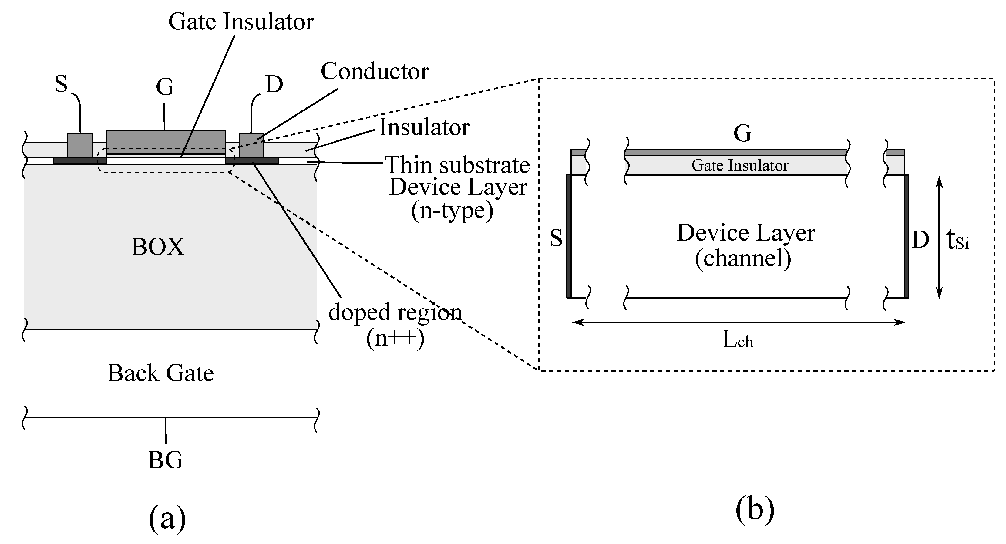
Figure 5c,d is not possible because these physical quantities lack of continuity. A more realistic profile for the charge and electron distributions are represented by the green profiles (smooth profile). Unfortunately, the real profiles of these two quantities do not allow for define a precise boundary for the depletion region, which to be identified must be approximated by using a simple model. In order to verify our previous qualitative analysis, we performed a few simulations of a 2D n-type PJLT by using COMSOL Multiphysics software. The geometrical dimensions of the simulated structure are shown in Figure 6.
The first simulation aimed to extract the “real” distribution of the electron concentration inside and outside the depletion region of the PJLT. By using the simulation results, we compared the real and the ideal electron concentration profile. Simulation results are shown in Figure 7.
Simulation results show an evident difference between the ideal electron concentration profiles representing the approximated analytical model and the simulated profiles. The main result from the analysis of these plots is that the electron concentration, inside the depletion region, is not zero and it can also reach significant values. This means that the formulas of the electric field and the electric potential distribution derived by using the hypothesis of complete depletion are affected by a certain amount of error, which may not be negligible. A qualitative analysis of the previous plots suggests that the greatest error of the analytical model occurs when the voltage approaches to V F B and V t h . In fact, if we analyze Figure 7a, we observe that the electron concentration in what is supposed to be the ideal depletion region is actually almost equal to the maximum value N D . Therefore, it is quite far from being completely depleted as the approximated analytical model claims. On the other hand, we observe in Figure 7e that the profile of the electron concentration inside the depletion region is similar to the ideal profile for values of V G , but they are not equal yet. In this case ( V G V t h ) the main source of error is due to the fact that the electron concentration outside the depletion region becomes so small that this region cannot be considered a good conductor as assumed by the analytical model. This was an important assumption, which allowed us to set zero electric field and zero electric potential at the boundary of the depletion region (see Appendix A). In conclusion, the main source of error of the approximated model consists in considering the term n n ( x ) = 0 x [ 0 , X d e p ] and n n ( x ) = N D x [ X d e p , t S i ] .
Similar observations could be extracted by analyzing the charge distribution inside the device layer, shown in Figure 8.
In order to quantify the error of the analytical model, we calculated the RMS error normalized with respect to N D for the concentration of the electrons inside ( ϵ R M S i ) and outside ( ϵ R M S o ) the depletion region by using the formulas in Equations (8) and (9).
ϵ R M S i = 1 N D 1 X d e p 0 X d e p n n 2 ( x ) d x x [ 0 , X d e p ]
ϵ R M S o = 1 N D 1 t S i X d e p X d e p t S i [ N D n n ( x ) ] 2 d x x [ X d e p , t S i ]
These RMS errors are plotted for different values of gate voltage and shown in Figure 9.
The previous plot shows that the error due to the approximation of complete depletion ( ϵ R M S i ) and the error due to the approximation of conductive device layer ( ϵ R M S o ) increase as soon as the gate voltage approaches to V F B and V t h , respectively. The maximum RMS error is approximately 90 % of N D , when the gate voltage approaches the threshold and the flat band voltage of the transistor.
Once the error introduced by the approximated model is quantified, we continued our analysis trying to extract a physical interpretation of this model. Figure 7 shows that the simulated charge density and electron concentration at the ideal boundary of the depletion region vary depending on the gate voltage applied. This trend is summarized in Figure 10.
The circles on each curve represent the electron concentration or the charge density at the ideal boundary of the depletion region, which was calculated by using Equation (4). Figure 10a shows that the electron concentration at the ideal boundary of the depletion region is not constant or equal to half of its maximum value, as common sense would suggest. Instead, the electron concentration at the boundary of the depletion region increases as the gate voltage approaches to V F B and decreases as the gate voltage approaches V t h . Between these two values, there is a voltage range in which the electron concentration at the ideal boundary of the depletion region is almost constant and approximately equal to 0.58 × 10 19 cm 3 . A similar observation can be made in Figure 10b for the charge density at the ideal boundary of the depletion region. Finally, we can conclude that the approximated analytical model describes the boundary of the depletion region, as a locus of points characterized by an electron concentration, which depends on the applied gate voltage. This dependency is a consequence of the fact that the profiles of the electron concentration and charge density diverge from the ideal profiles, when the voltage approaches to V F B and V t h .
During our analysis, we observed that a definition of the depletion region boundary in terms of electron concentration has one major advantage with respect to the definition based on spatial position described by Equation (4). The definition based on electron concentration can be used to determine the boundary of the depletion region also for the cases where the drain and source terminals are not grounded. In fact, in this case, the boundary of the depletion region is bent due to the variation of electric potential along the channel and this phenomenon is not taken into account by Equation (4). For this reason, we tried to extract an analytical formula, which describes the dependency of the electron concentration (and charge density) at the boundary of the depletion region with respect to the applied gate voltage. First of all, we joined the circles in Figure 10 with straight lines as shown in Figure 11a,b. Then, we approximated these curves with polynomial functions. We observed that the relative error between the curves in Figure 11a,b and their polynomial approximation drop to a few percentage points when the order of the polynomial function approaches the eighth order as shown in Figure 11c,d.
The analysis of the plots in Figure 11c,d shows that a good approximation of the data in Figure 11a,b is obtained by using a polynomial function of the eighth order, which provides a relative error of less than 1 % . The eighth order polynomial formulas for n n ( X d e p ) and ρ ( X d e p ) are shown in Equations (10) and (11):
n n ( X d e p ) 8 t h = [ 1.1127 + 2.0256 V G + 3.5541 V G 2 + 3.5545 V G 3 + 2.1561 V G 4 + + 0.8023 V G 5 + 0.1782 V G 6 + 0.0216 V G 7 + 0.0011 V G 8 ] × 10 19 ,
ρ ( X d e p ) 8 t h = 0.1806 3.2454 V G 5.6943 V G 2 5.6949 V G 3 3.4544 V G 4 1.2855 V G 5 0.2854 V G 6 0.0346 V G 7 0.0017 V G 8 .
We can use these two equations for detecting the boundary of the depletion region for any value of gate voltage. Furthermore, these formulas can be used to provide a graphical representation of the depletion region boundary from the numerical results obtained in COMSOL Multiphysics. This includes also the cases where the drain is not grounded as shown in Figure 12.
Finally, we wanted to compare the approximated analytical model with another one derived by our own “common sense”. The “common sense” model is based on the assumption that the electron concentration at the boundary of the depletion region can be assumed to be half of the donor concentration inside the device layer. This represents the most intuitive model of the depletion region width. The electron concentrations at the depletion region boundary defined by the common sense threshold are circled and shown in Figure 13a.
By using the x-coordinates of the “circles” drawn in Figure 13a and the voltages associated with the curves over which each circle lay, we can draw the red continuous line shown in Figure 13b. This curve represents the depletion region width model derived by using common sense. In the same plot, we drew a dashed line, which represents the analytic model that we investigated in this paper. First of all, we notice that the analytic model and the “common sense” model estimate two different values of depletion region width, when the same gate voltage is applied to the transistor. The two curves seem to follow a similar trend in the middle range of the gate voltage, although they are separated by an offset value. The “common sense” model predicts that the transistor should turn off when V G = 4.05 V, and it should turn on when V G = 0.39 V. These values are quite different than the OFF and ON voltage predicted by the approximated analytic model ( V t h 4.5 V and V F B = 0.026 V). Finally, by comparing the electron concentration profiles at the on and off voltages of these two models (Figure 13a and Figure 10a), we find out that the approximated analytic model is the one that provides an electron concentration profile, which resembles better the ideal profile. In fact, if we compare the electron concentration profiles extracted at the off voltage of these two models, then we can observe that the electron concentration profile predicted by the “common sense model” (curve in Figure 13a for V G 4 V) is much larger than the one predicted by the approximated analytical model (curve in Figure 10a for V G 4.5 V). This means that the substrate of the transistor is more conductive at the off voltage predicted by the “common sense” model, thus the off state of the transistor is better approximated if we estimate the depletion region width by using the approximated analytical model. A similar consideration can be done when we analyze the electron concentration profiles at the on voltages associated with the two models. We conclude that the “common sense” model is less accurate than the analytic model, when the transistor approaches the on and off state. However, the “common sense” model still represents a good approximation when the gate voltage is far from the on and off voltage values.

5. Conclusions

In this paper, we analyzed and quantified the error introduced by the approximated model, which is widely used to describe the depletion region width of junctionless transistors. The analysis was supported by numerical simulations performed in COMSOL Multiphysics software. Simulation results of an N-type PJLT showed that the analytical model is affected by a significant error when the gate voltage approaches the threshold voltage or when it approaches the flat-band voltage of the transistor. In these two extreme cases, the RMS error of the electron concentration profile inside and outside the depletion region was calculated to be approximately 90 % of the donor concentration inside the substrate of the transistor. This proves that the approximated analytical model does not provide an accurate formula to calculate the values of the flat-band and threshold voltages of the transistor. Furthermore, we found out that the approximated analytical model of the depletion region width defines the depletion region boundary characterized by a value of electron concentration, which depends on the applied gate voltage. This dependency was analytically extracted by using an eighth order polynomial function. Finally, we proved that this polynomial formula is as useful as the initial analytical model because it can be utilized to determine the position of the depletion region boundary in numerical simulations, when the drain and source terminals are not grounded.

Author Contributions

Conceptualization, A.N. and L.M.; methodology, L.M.; software, A.N.; validation, A.N., L.M., M.N.A., and A.R.; formal analysis, A.N.; investigation, A.N.; resources, A.N.; data curation, A.N. and L.M.; writing—original draft preparation, A.N.; writing—review and editing, A.N., L.M, A.R., and M.N.A.; visualization, A.N. and L.M.; supervision, L.M. and A.R.; project administration, L.M.

Funding

This research was funded by the University of Southeastern Norway.

Conflicts of Interest

The authors declare no conflict of interest.The funders had no role in the design of the study; in the collection, analyses, or interpretation of data; in the writing of the manuscript, or in the decision to publish the results.

Appendix A. Depletion Region Width Analytical Formula

The purpose of this appendix is to clarify the procedure utilized to derive the analytical model of the depletion region width in a PJLT. The structure analyzed in this paper is an n-type PJLT connected in capacitor configuration as shown in Figure A1.
Figure A1. N-type PJLT ideal physical structure.
Electronics 08 01436 g0a1
In this analysis, we assume that the PJLT device layer has been uniformly doped, which means that N D ( x ) = c o n s t a n t = N D . In addition, we assume that the drain and source terminals are sufficiently far from each other that the depletion region in the middle of the device layer can be considered flat or uniform. By using the previous assumptions, we can extract an analytical formula for the depletion region width by solving the Poisson equation, shown in Equation (A1):
d 2 ϕ ( x ) d 2 x = ρ ( x ) ϵ S i = q ( p n ( x ) n n ( x ) + N D + ( x ) ) ϵ S i x [ 0 , X X d e p ] ,
where: ϕ ( x ) , ρ ( s ) , n n ( x ) , N D + ( x ) and p n ( x ) are the distribution of the electric potential, the distribution of the charge density, the distribution of the concentration of electrons, the distribution of the positive ion concentration due to the impurities in the substrate, and the distribution of the hole concentration, respectively, all evaluated along the symmetric axis of the transistor inside its depletion region. Furthermore, ϵ S i is the dielectric constant of the silicon substrate and q is the elementary charge + 1.6 × 10 19 C . The concentrations n n ( x ) and p n ( x ) can be rewritten by using the Shockley Equations as shown in Equations (A2) and (A3):
n n ( x ) = n i e E F E F i + q ϕ ( x ) k B T = N D e + q ϕ ( x ) k B T = N D e + ϕ ( x ) V t ,
p n ( x ) = n i 2 n n ( x ) = n i 2 N D e ϕ ( x ) V t ,
where: E F is the Fermi level of the doped semiconductor, E F i is the intrinsic Fermi level, n i is the intrinsic concentration of electrons, and V t = k B T / q is the thermal voltage. Unfortunately, by substituting Equation (A2) and (A3) in Equation (A1), we find that the Poisson equation cannot provide an analytical solution. Nevertheless, a common method to overcome this problem consists of using the hypothesis of complete depletion ( n n ( x ) 0 if x [ 0 , X d e p ] and n n ( x ) N D if x [ X d e p , t S i ] ), along with the hypothesis of complete ionization ( N D + = N D ) and negligible concentration of the minority carriers ( p n ( x ) = 0 ) during the whole operation of the transistor. In this case, the equation simplifies as shown in Equation (A4):
d 2 ϕ ( x ) d 2 x q N D ϵ S i , x [ 0 , X d e p ] .
Finally, this approximated form of the Poisson equation can be analytically solved. From the Poisson Equation, we can extract Equation (A5), by using the known relation Φ ( x ) = E :
d E x ( x ) d x = q N D ϵ S i .
Next, by integrating Equation (A5) once, we can find the general solution for the electric field inside the device layer shown in Equation (A6):
E x ( x ) = q N D ϵ S i x + c 1 .
By integrating Equation (A6) once more, we obtain the general solution for the electrical potential inside the device layer as shown in Equation (A7):
ϕ ( x ) = q N D 2 ϵ S i x 2 c 1 x + c 2 ,
where: c 1 and c 2 are arbitrary constants. To find the value of these two arbitrary constants, we need to define two boundary conditions. The first one can be found by evaluating the electric potential at the interface between the device layer and the thin gate insulating layer. This interface corresponds to the potential at x = 0 . The electrical potential in this point is usually known as surface potential ϕ s , which can be expressed as shown in Equation (A8):
ϕ s = V G V F B V O X ,
where: V G is the electric potential at the gate terminal and V O X is the drop voltage across the thin gate insulating layer. A useful formula of V O X is shown in Equation (A9). This one can be calculated by integrating the electric field across the oxide, which separates the metal from the device layer:
V O X = q N D C o x X d e p .
On the other hand, the flat band voltage can be calculated by using the formula in Equation (A10) for an n-type PJLT and the formula in Equation (A11) for a p-type PJLT:
V F B , n = q Φ M q Φ s n = q Φ M ( q χ + E g / 2 q Φ n ) ,
V F B , p = q Φ M q Φ s p = q Φ M ( q χ + E g / 2 + q Φ p ) ,
where: q Φ M is the gate work function, q χ is the electron affinity, E g is the energy band gap, and q Φ n , p is the bulk potential that is defined as k B T l n ( N D , A / n i ) , k B is the Boltzmann constant, and T is the temperature.
A second boundary condition can be found by introducing an additional approximation, which consists of assuming that the device layer behaves like an ideal conductor. If we consider the doping of the device layer sufficiently high to mimic the behavior of an ideal conductor, then we can assume that the electric field created by the gate electrode becomes zero ( E x ( X d e p ) = 0 ) at the boundary of the depletion region. In addition, the electric potential at the boundary of the depletion region is also zero because the device layer has been electrically grounded through the drain and the source terminal ( ϕ ( X d e p ) = 0 ). By using ϕ ( x = 0 ) = ϕ s and E ( x = X d e p ) = 0 , we can solve the system of equations shown in Equation (A12) [12]:
E x ( x ) = q N D ϵ S i x + c 1 , ϕ ( x ) = q N D 2 ϵ S i x 2 c 1 x + c 2 , E ( X d e p ) = 0 , ϕ ( 0 ) = ϕ s .
The particular solutions of the system are shown in Equation (A13):
E x ( x ) = q N D ϵ S i ( x X d e p ) , ϕ ( x ) = ϕ s + q N D ϵ S i X d e p x q N D 2 ϵ S i x 2 ,
where the arbitrary constants were found to be: c 1 = q N D ϵ S i X d e p and c 2 = ϕ s . Finally, by evaluating the electric potential in x = X d e p at which ϕ ( X d e p ) = 0 and by using Equations (A8) and (A9) in Equation (A13), we can find the formula of the depletion region width shown in Equation (A14):
X d e p = ϵ S i C O X + ( ϵ S i C O X ) 2 2 ϵ S i q N D ( V G V F B ) .
A similar procedure can be used to derive the formula of the depletion region for a p-type PJLT. The formula for this case is shown in Equation (A15):
X d e p = ϵ S i C O X + ( ϵ S i C O X ) 2 + 2 ϵ S i q N A ( V G V F B ) .

References

  1. Lilienfeld, J. Method and Apparatus for Controlling Electric Currents. U.S. Patent 1745175, 22 October 1925. [Google Scholar]
  2. Colinge, J.P.; Lee, C.W.; Afzalian, A.; Akhavan, N.D.; Yan, R.; Ferain, I.; Razavi, P.; O’neill, B.; Blake, A.; White, M.; et al. Nanowire transistors without junctions. Nat. Nanotechnol. 2010, 5, 225. [Google Scholar] [CrossRef] [PubMed]
  3. Ionescu, A.M. Electronic devices: Nanowire transistors made easy. Nat. Nanotechnol. 2010, 5, 178. [Google Scholar] [CrossRef] [PubMed]
  4. Lee, C.W.; Afzalian, A.; Akhavan, N.D.; Yan, R.; Ferain, I.; Colinge, J.P. Junctionless multigate field-effect transistor. Appl. Phys. Lett. 2009, 94, 053511. [Google Scholar] [CrossRef]
  5. Colinge, J.; Lee, C.; Akhavan, N.D.; Yan, R.; Ferain, I.; Razavi, P.; Kranti, A.; Yu, R. Junctionless transistors: Physics and properties. In Semiconductor-On-Insulator Materials for Nanoelectronics Applications; Springer: Berlin, Germany, 2011; pp. 187–200. [Google Scholar]
  6. Rudenko, T.; Nazarov, A.; Yu, R.; Barraud, S.; Cherkaoui, K.; Razavi, P.; Fagas, G. Electron mobility in heavily doped junctionless nanowire SOI MOSFETs. Microelectron. Eng. 2013, 109, 326–329. [Google Scholar] [CrossRef]
  7. Han, M.H.; Chang, C.Y.; Chen, H.B.; Cheng, Y.C.; Wu, Y.C. Device and circuit performance estimation of junctionless bulk FinFETs. IEEE Trans. Electron Devices 2013, 60, 1807–1813. [Google Scholar] [CrossRef]
  8. Han, M.H.; Chang, C.Y.; Jhan, Y.R.; Wu, J.J.; Chen, H.B.; Cheng, Y.C.; Wu, Y.C. Characteristic of p-type junctionless gate-all-around nanowire transistor and sensitivity analysis. IEEE Electron Device Lett. 2013, 34, 157–159. [Google Scholar] [CrossRef]
  9. Jenifer, I.; Vinodhkumar, N.; Srinivasan, R. Optimization of Bulk Planar Junctionless Transistor using Work function, Device layer thickness and Channel doping concentration with OFF Current constraint. In Proceedings of the 2016 Online International Conference on Green Engineering and Technologies (IC-GET), Coimbatore, India, 19 November 2016; pp. 1–3. [Google Scholar]
  10. Baruah, R.K.; Paily, R.P. Analog performance of bulk planar junctionless transistor (BPJLT). In Proceedings of the 2012 Third International Conference on Computing, Communication and Networking Technologies (ICCCNT’12), Coimbatore, India, 26–28 July 2012; pp. 1–4. [Google Scholar]
  11. Gundapaneni, S.; Ganguly, S.; Kottantharayil, A. Bulk planar junctionless transistor (BPJLT): An attractive device alternative for scaling. IEEE Electron Device Lett. 2011, 32, 261–263. [Google Scholar] [CrossRef]
  12. Lin, H.C.; Lin, C.I.; Lin, Z.M.; Shie, B.S.; Huang, T.Y. Characteristics of planar junctionless poly-Si thin-film transistors with various channel thickness. IEEE Trans. Electron Devices 2013, 60, 1142–1148. [Google Scholar] [CrossRef]
  13. Duarte, J.P.; Choi, S.J.; Moon, D.I.; Choi, Y.K. Simple analytical bulk current model for long-channel double-gate junctionless transistors. IEEE Electron Device Lett. 2011, 32, 704–706. [Google Scholar] [CrossRef]
  14. Ghosh, B.; Akram, M.W. Junctionless tunnel field effect transistor. IEEE Electron Device Lett. 2013, 34, 584–586. [Google Scholar] [CrossRef]
  15. Ytterdal, T.; Cheng, Y.; Fjeldly, T. Device Modeling for Analog and RF CMOS Circuit Design; Wiley: Hoboken, NJ, USA, 2003. [Google Scholar]
  16. Deva Sarma, K.C.; Sharma, S. A method for determination of depletion width of single and double gate junction less transistor. In Proceedings of the 2015 International Conference on Electronic Design, Computer Networks Automated Verification (EDCAV), Bari, Italy, 22–25 September 2015; pp. 114–119. [Google Scholar] [CrossRef]
  17. Pavanello, M.A.; Trevisoli, R.; Doria, R.T.; de Souza, M. Static and dynamic compact analytical model for junctionless nanowire transistors. J. Phys. Condens. Matter 2018, 30, 334002. [Google Scholar] [CrossRef]
  18. Liu, F.Y.; Liu, H.Z.; Liu, B.W.; Guo, Y.F. An analytical model for nanowire junctionless SOI FinFETs with considering three-dimensional coupling effect. Chin. Phys. B 2016, 25, 047305. [Google Scholar] [CrossRef]
  19. Chaudhary, T.; Khanna, G. A 2D Potential Based Threshold Voltage Model Analysis and Comparison of Junctionless Symmetric Double Gate Vertical Slit Field Effect Transistor. IETE J. Res. 2017, 63, 451–460. [Google Scholar] [CrossRef]
  20. COMSOL Multiphysics, version 5.3; COMSOL AB: Stockholm, Sweden, 2017.
  21. Huda, A.; Arshad, M.M.; Othman, N.; Voon, C.; Ayub, R.; Gopinath, S.C.; Foo, K.; Ruslinda, A.; Hashim, U.; Lee, H.C.; et al. Impact of size variation in junctionless vs junction planar SOI n-MOSFET transistor. In Proceedings of the 2015 IEEE Regional Symposium on Micro and Nanoelectronics (RSM), Kuala Terengganu, Malaysia, 19–21 August 2015; pp. 1–4. [Google Scholar]
  22. Cheng, K.; Khakifirooz, A. Fully depleted SOI (FDSOI) technology. Sci. China Inf. Sci. 2016, 59, 061402. [Google Scholar] [CrossRef]
  23. Grove, A.S. Physics and Technology of Semiconductor Devices; Wiley: Hoboken, NJ, USA, 1967; Chapter 4. [Google Scholar]
  24. Adnan, M.M.R.; Khosru, Q.D.M. A Simple Analytical Model of Threshold Voltage for P-Channel Double Gate Junctionless Transistor. In Proceedings of the 2018 IEEE International Conference on Electron Devices and Solid State Circuits (EDSSC), Shenzhen, China, 6–8 June 2018; pp. 1–5. [Google Scholar] [CrossRef]
  25. Wagaj, S.; Chavan, Y.; Patil, S. A Two-dimensional Analytical Model and Simulation for Dual Material Gate Junctionless Transistor. In International Conference on Communication and Signal Processing 2016 (ICCASP 2016); Atlantis Press: Paris, France, 2016. [Google Scholar] [CrossRef]
  26. Jiang, C.; Liang, R.; Wang, J.; Xu, J. A two-dimensional analytical model for short channel junctionless double-gate MOSFETs. AIP Adv. 2015, 5, 057122. [Google Scholar] [CrossRef]
  27. Roy, D.; Biswas, A. Analytical model of nanoscale junctionless transistors towards controlling of short channel effects through source/drain underlap and channel thickness engineering. Superlattices Microstr. 2018, 113, 71–81. [Google Scholar] [CrossRef]
  28. Singh, S.; Raj, B.; Vishvakarma, S. Analytical modeling of split-gate junction-less transistor for a biosensor application. Sens. Bio-Sens. Res. 2018, 18, 31–36. [Google Scholar] [CrossRef]
  29. Fabiha, R.; Saha, C.N.; Islam, M.S. Analytical modeling and performance analysis for symmetric double gate stack-oxide junctionless field effect transistor in subthreshold region. In Proceedings of the 2017 IEEE Region 10 Humanitarian Technology Conference (R10-HTC), Dhaka, Bangladesh, 21–23 December 2017; pp. 310–313. [Google Scholar] [CrossRef]
  30. Pratap, Y.; Kumar, M.; Kabra, S.; Haldar, S.; Gupta, R.S.; Gupta, M. Analytical Modeling of Gate-all-around Junctionless Transistor Based Biosensors for Detection of Neutral Biomolecule Species. J. Comput. Electron. 2018, 17, 288–296. [Google Scholar] [CrossRef]
  31. Hu, G.; Xiang, P.; Ding, Z.; Liu, R.; Wang, L.; Tang, T. Analytical Models for Electric Potential, Threshold Voltage, and Subthreshold Swing of Junctionless Surrounding-Gate Transistors. IEEE Trans. Electron Devices 2014, 61, 688–695. [Google Scholar] [CrossRef]
  32. Ávila Herrera, F.; Paz, B.; Cerdeira, A.; Estrada, M.; Pavanello, M. Charge-based compact analytical model for triple-gate junctionless nanowire transistors. Solid-State Electron. 2016, 122, 23–31. [Google Scholar] [CrossRef]
Figure 1. N-type PJLT physical structure; (a) complete structure on FDSOI wafer; (b) simplified model of the JLT physical structure.
Electronics 08 01436 g001
Figure 2. N-type PJLT capacitor.
Electronics 08 01436 g002
Figure 3. N-type PJLT working principle. (a) state of the PJLT for a generic value of gate voltage; (b) depletion region for different values of gate voltage.
Electronics 08 01436 g003
Figure 4. Analytical depletion width as a function of the gate voltage computed with the data in Table 1. (a) N-type PJLT; (b) P-type PJLT.
Electronics 08 01436 g004
Figure 5. Profiles of the main parameters characterizing the depletion region in an n-type PJLT. (a) PJLT in capacitor configuration with source and drain sufficiently far from each other to consider the depletion region boundary uniform in the middle of the device layer; (b) impurity ions distribution inside the device layer (complete ionization); (c) carrier distribution inside the device layer (blue line = hole distribution, green line = real electron distribution, red line = ideal electron distribution); (d) charge density inside the device layer ( green line = real charge density distribution, red line = ideal charge density distribution).
Electronics 08 01436 g005
Figure 6. Geometrical dimensions of the simulated n-type PJLT.
Electronics 08 01436 g006
Figure 7. Comparison between the ideal and the simulated electron concentration inside the device layer, for different values of gate voltage. The parameter of the simulated structure are shown in Table 1. The PJLT was electrically connected as shown in Figure 3. x = 0 is placed at the interface S i O 2 /substrate. (a) Profiles for V G = 0.25 V. (b) Profiles for V G = 0.75 V. (c) Profiles for V G = 2 V. (d) Profiles for V G = 3 V. (e) Profiles for V G = 4 V. (f) Profiles for V G = 4.5 V.
Electronics 08 01436 g007
Figure 8. Comparison between the ideal and the simulated charge density inside the device layer, for different values of gate voltage. The parameters of the simulated structure are shown in Table 1. The PJLT was electrically connected as shown in Figure 3. x = 0 is place at the interface S i O 2 /substrate. (a) Profiles for V G = 0.25 V. (b) Profiles for V G = 0.75 V. (c) Profiles for V G = 2 V. (d) Profiles for V G = 3 V. (e) Profiles for V G = 4 V. (f) Profiles for V G = 4.5 V.
Electronics 08 01436 g008
Figure 9. RMS error between the ideal and the simulated electron concentration profile inside ( ϵ R M S i ) and outside ( ϵ R M S o ) the depletion region, normalized in respect to N D .
Electronics 08 01436 g009
Figure 10. (a) electron concentration profiles for different values of gate voltage; (b) charge density profiles for different values of gate voltage. The circles represents the value of electron concentration and charge density at the ideal boundary of the depletion region. The gate voltage was swept in the range [−0.25 V,−4.5 V] with a step of 0.25 V.
Electronics 08 01436 g010
Figure 11. (a) electron concentration at the boundary of the ideal depletion region for different values of gate voltage; (b) charge density at the boundary of the ideal depletion region for different values of gate voltage; (c) relative error between the data in (a) and polynomial approximations of fourth, sixth, and eighth order; (d) relative error between the data in (b) and polynomial approximations of fourth, sixth, and eighth order. The gate voltage was swept in the range [−0.25 V,−4.5 V] with a step of 0.25 V.
Electronics 08 01436 g011
Figure 12. Electron concentration generated by COMSOL Multiphysics. V G = 2 V and V D = 3 V. The black line represents the boundary of the depletion region. (a) whole PJLT; (b) zoom on a specific area of the PJLT.
Electronics 08 01436 g012
Figure 13. Comparison between the “common sense” model and the approximated analytic model. (a) detection of the electron concentration at the boundary of the depletion region defined by the “common sense” model for different values of gate voltage; (b) comparison between the depletion region estimated by the “common sense” model and the depletion region estimated by using the approximated analytic model described in Equation (4). The gate voltage was swept in the range [−0.25 V,−4.5 V] with a step of 0.25 V.
Electronics 08 01436 g013
Table 1. Depletion PJLT parameters.
n-Type PJLTp-Type PJLT
ParameterValue
Materials
Device layerSi/n-typeSi/p-type
insulating gate layer S i O 2
Gate electrodeN-type Poly-SiP-type Poly-Si
Material proprieties
Device layer Doping concentration (atoms/cm 3 ) N D = 10 19 N A = 3.05 × 10 18
Intrinsic carrier concentration: n i (atoms/cm 3 ) 5.4 × 10 9 at 293.15 K
Dielectric constant device layer: ϵ S i (F/cm) 11.7 ϵ 0
Dielectric constant insulator: ϵ o x (F/cm) 3.9 ϵ 0 ( S i O 2 )
Dimensions
Channel length: L c h (nm)500
Device layer thickness: t S i (nm)10
Gate oxide thickness: t o x (nm)8
Derived Parameters
Electron affinity: q χ (eV)4.05
Energy band gap: E g (eV)1.13
Bulk potential: q Φ n , p = k B T l n ( N D , A / n i ) (eV)0.5390.509
Oxide capacitance per unit area: C o x = ϵ o x / t o x (F/cm 2 ) 4.32 × 10 7
Gate work function: q Φ M (eV)4.05 (PolySi/n-type)5.15 (PolySi/p-type)
Flat Band Voltage: V F B (V)−0.0260.026

