Abstract
With the continual increasing application requirements of broadband vibration energy harvesters (VEHs), many attempts have been made to broaden the bandwidth. As compared to adopted only a single approach, integration of multi-approaches can further widen the operating bandwidth. Here, a novel two-degree-of-freedom cantilever-based vibration triboelectric nanogenerator is proposed to obtain high operating bandwidth by integrating multimodal harvesting technique and inherent nonlinearity broadening behavior due to vibration contact between triboelectric surfaces. A wide operating bandwidth of 32.9 Hz is observed even at a low acceleration of 0.6 g. Meanwhile, the peak output voltage is 18.8 V at the primary resonant frequency of 23 Hz and 1 g, while the output voltage is 14.9 V at the secondary frequency of 75 Hz and 2.5 g. Under the frequencies of these two modes at 1 g, maximum peak power of 43.08 μW and 12.5 μW are achieved, respectively. Additionally, the fabricated device shows good stability, reaching and maintaining its voltage at 8 V when tested on a vacuum compression pump. The experimental results demonstrate the device has the ability to harvest energy from a wide range of low-frequency (<100 Hz) vibrations and has broad application prospects in self-powered electronic devices and systems.
1. Introduction
As a result of the rapid development of information technology and the electronics industry, many small-scale electronic devices with low power consumption have emerged. Energy harvesting technology that converts the ambient available energy into electrical energy to power these devices is the best way to overcome the limitation of traditional battery power supply [1,2,3,4]. Mechanical vibration energy, as compared with other kinds of existing energy sources, is the most ubiquitous and popular in our daily life [5]. With the help of electromechanical mechanisms, including piezoelectric [6,7], electrostatic [8,9], electromagnetic [10,11], and triboelectric [12,13,14,15,16], wasted mechanical energy from vibrations is transformed into useful electrical power.
Currently, most vibrational energy harvesters (VEHs) are usually designed as resonance systems for higher power output. However, one of the main problems for VEHs with the resonant behavior is the narrow operating bandwidth. Thus, when operated under irregular mechanical vibration sources with low and variable frequencies, most VEHs yield very low and irregular output power, which lowers their practical application possibilities.
To solve the problem of narrow bandwidth, many researchers have demonstrated some broadband harvesters by applying multimodal harvesting technique [17,18,19,20,21,22,23]. Multimodal energy harvesters are considered more efficient in matching multiple frequencies to better utilize kinetic energy. Sari et al. [17], Liu et al. [18], and Qi et al. [19] reported the use of multiple cantilevers or a cantilever array as one solution to increase the bandwidth. However, this type of energy harvester has the disadvantage of being bulky and complex in structure, thus overshadowing its advantages in broadband behavior. Another multimodal system was developed with multiple bending modes in a continuous beam, rather than using arrays of cantilevers configuration [20,21,22,23]. Ou et al. presented a broadband energy harvester with a two-mass cantilever beam structure [20]. Due to the addition of an extra mass, two useful working modes can be obtained. Arafa et al. developed a two-degree-of-freedom (2DOF) cantilever-based piezoelectric generator which used the proof mass as a dynamic amplifier [21]. However, the multimodal harvester only increases the number of peak amplitudes, and the bandwidth of each peak is relatively narrow, which still causes a sharp drop in power generation when the excitation vibration frequency does not match the natural frequency of the harvester.
Meanwhile, other researchers have adopted different nonlinearities to enhance wideband energy harvesting, especially impact-induced nonlinearity. In this case, a mechanical stopper is usually mounted on these devices, which is used to limit the motion amplitude of vibrations, resulting in nonlinear stiffness. Soliman et al. [24] developed a broadband microelectromagnetic energy harvester by changing the stiffness of the resonator with a mechanical stopper. On the basis of a similar idea, Liu et al. [25,26] also realized broadband piezoelectric MEMS energy harvesters by using the assembled metal package and cantilever as mechanical stoppers. Although the above electromagnetic and piezoelectric energy harvesters realize the wideband mechanism, the approach needs special arrangements of stoppers.
Unlike other energy harvesting technologies, vibration triboelectric nanogenerator (VTENG) has the inherent nonlinear characteristic between the triboelectric layers due to the working mechanism involving repeated contact and separation, which makes it well suited for broadband operation using impact vibration energy harvesting. Furthermore, the triboelectric mechanism shows other advantages including simple structure, low cost, high energy conversion efficiency, and outstanding output power density [27,28]. In recent years, many VTENGs with impact nonlinearity have been proposed and the three main types of these devices are based on helical coil springs [29,30], fixed-fixed beam springs [31,32], and cantilever beam springs [33,34,35]. However, almost all of the researchers working on VTENG with impact nonlinearity have focused on the 1DOF vibration system, and therefore the operating bandwidth of these proposed devices is still limited.
In this study, a novel VTENG with a compact 2DOF cantilever structure is proposed to achieve wide operating bandwidth at low frequency by integrating the multimodal harvesting technique and the inherent impact-engaged nonlinearity due to the mutual contact of triboelectric surfaces caused by the cantilever motion. The fabrication of the designed VTENG is discussed and the effects of different PDMS microstructures on the output performance of triboelectric devices are studied. Finally, the output performance of the fabricated device with typical dimensions is tested and evaluated.
2. Design and Analysis
2.1. Device Configuration
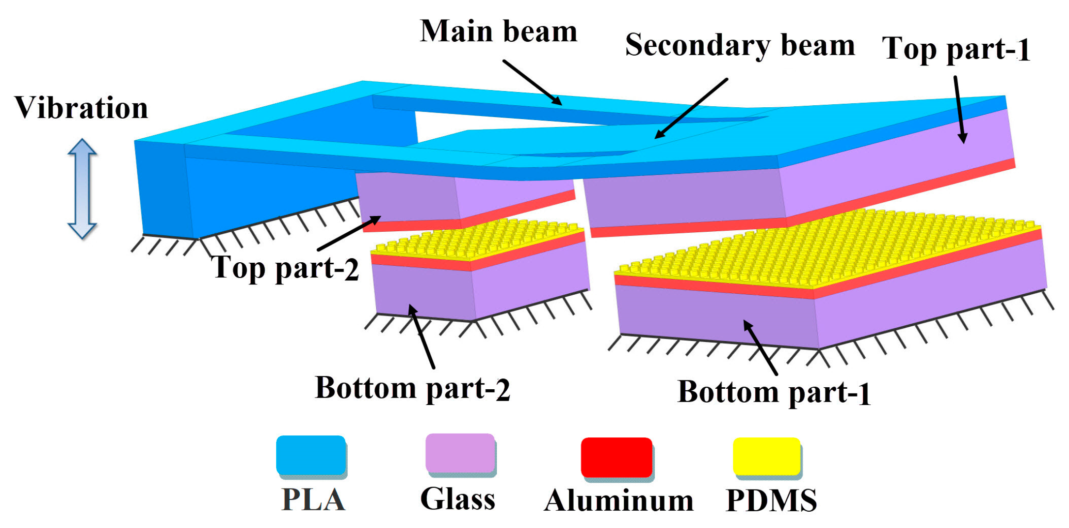
As shown in Figure 1, the schematic structure of the designed broadband VTENG is a cantilever structure (including one main beam and one inner secondary beam) comprised of two top parts attached at the ends of the main and secondary beams as proof masses, and two corresponding bottom parts. The energy is conversed when the triboelectric layers on the top and bottom parts contact and separate periodically. The top part is comprised of both a glass substrate and an aluminum thin film as one triboelectric layer and a top electrode on the substrate, while the bottom part is comprised of a PDMS thin film with microstructures as another triboelectric layer, an aluminum thin film as the bottom electrode, and a glass substrate. Meanwhile, as shown in Figure 1, the designed VTEH consists of two triboelectric elements. Here, the two triboelectric elements are called the main triboelectric nanogenerator (TENG) including top part-1 and bottom part-1, and the secondary TENG including top part-2 and bottom part-2. Once the base of the VTENG starts to vibrate, the main beam and secondary beam act as a spring of the main TENG and the secondary TENG, respectively, to transfer the vibrational energy from environment to active triboelectric surfaces.

Figure 1.
Schematic for the broadband vibration triboelectric nanogenerator.
2.2. Principle of Operation
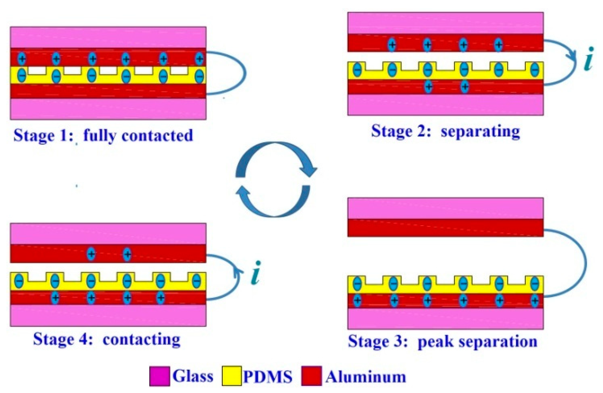
As mentioned above, the VTENG includes the main TENG and secondary TENG, and their working principle is the coupling effect of contact charging and electrostatic induction, the detailed process is shown in Figure 2. In the initial configuration, before applying the mechanical vibration, the top and bottom parts maintain a separation distance without any prior charges. When the mechanical vibration is applied, the top part contacts the bottom part where the two surfaces of top aluminum and PDMS with microstructures rub each other and electrification starts. Because aluminum is much more triboelectrically positive than PDMS, the aluminum surface will be positively charged and the PDMS surface with microstructures will be negatively charged (Figure 2, Stage 1). Once the top part begins to separate from the fixed bottom part, as a result of the vibrating motion of the beams, the electrons transferred from the bottom aluminum beneath the PDMS layer to the aluminum layer of the top part (opposite to the current direction shown in Figure 2, Stage 2). This current continues until the distance between the top part and bottom part reaches maximum where the beams reach the other end of the vibration period (Figure 2, Stage 3). At this time, the electrons stop flowing due to the electrostatic equilibrium. Thereafter, the top part begins to move closer to the bottom part, which breaks the electrostatic equilibrium between the two parts. The electrons start flowing in the opposite direction because of the potential difference (Figure 2, Stage 4). Most of the positive charges on the bottom aluminum electrode flow back to the top aluminum electrode at the moment when the top and bottom parts contact again (Figure 2, Stage 1).

Figure 2.
Operating mechanism for the VTENG (for simplicity the beam is not shown).
2.3. Theoretical Analysis
In the aforementioned process, the VTENG works at a vertical contact-separation mode and the potential difference between the aluminum electrodes for the main TENG or secondary TENG can be calculated as [36]:
where Q is the charge transferred through the external circuit, S is the contact area of the triboelectric layers, ε0 is the dielectric constant of air, εP is the relative dielectric constant of PDMS, δ is the thickness of the patterned PDMS thin film, d is the initial distance between top electrode and top surface of the PDMS film, zi(t) is the relative displacement of the top electrode with respect to PDMS layer, and σ is the surface charge density of the patterned PDMS film.
When the VTENG works in the vertical contact separation mode, the vibration system has two motion states, i.e., before impact when Zi(t) < d and at impact when Zi(t) > d. The frequency response characteristics of a similar 1DOF VTENG with impact nonlinearity have already been fully revealed by previous studies [29,30,31]. According to these studies, we know that the relative displacement amplitude in free vibration and the natural frequency of the driving beam itself are two important parameters. This is because the relative displacement amplitude is related to the operating bandwidth and output performance of the device, and the natural frequency of the drive beam determines the range of the frequency. Therefore, here, we mainly investigate the effects of various system parameters on the relative displacement amplitude before impact and the natural frequency of the system to provide an important design guideline.
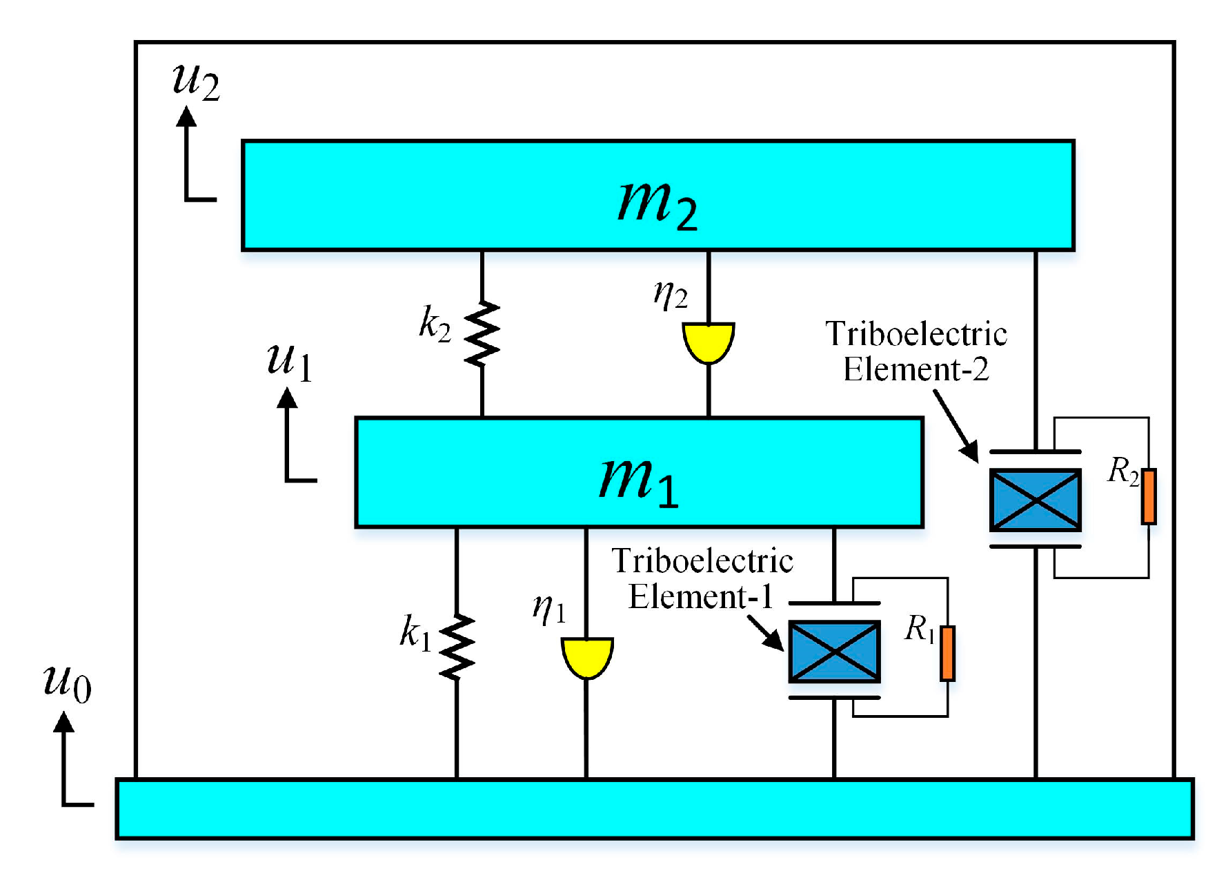
The vibrational model of the proposed VTENG can be regarded as a 2DOF lumped-mass system subjected to base excitation under a no-impact state, as shown in Figure 3, which consists of the main mass m1 and secondary mass m2, mechanical damping η1 and η2, and spring stiffness k1 and k2. The governing equations of this 2DOF system can be derived as:
where u0, u1, and u2(t) are the displacements of the base, mass m1, and mass m2, respectively; Fe1 and Fe2 are the electrostatic forces of the triboelectric element-1 and element-2 (i.e., the main TENG and secondary TENG of the device), respectively, which can be given by [31,37]:
where S1 and S2 are the contact areas of the main TENG and secondary TENG, V1 and V2 are the output voltages of the two TENGs, and R1 and R2 are the load resistance of the two triboelectric elements. The modeling mainly aims to display the mechanism for two comparable peaks that are obtained at two resonant low frequencies by carefully controlling the spring-mass parameters. Therefore, the triboelectric forces (Fe1 and Fe2) will not be considered in the current study. Meanwhile, it is obvious that zi (t) (i = 1, 2) in Equation (1) is the relative displacement of the inertial mass m1 and m2, respectively, i.e., z1(t) = u1 − u0 and z2(t) = u2 − u0. Rearranging them to Equation (2), we now obtain:

Figure 3.
Lumped-mass model of proposed 2DOF VTENG under a no-impact state.
Letting
Applying Laplace transform to Equation (4), solving it and applying s = jω, the relative displacements of the inertial mass m1 and m2 can be obtained as
As shown in Equations (1)–(6), the parameters affecting the performance of the proposed VTENG include material properties of triboelectric layers, the mass ratio m2/m1, the natural frequency ratio ω2/ω1, and the damping ratios ζ1 and ζ2, etc. Here, m1 and m2 are the masses of top part-1 and top part-2 of the designed VTENG, and ω1 and ω2 can be adjusted by changing the parameters of m1, m2, k1, and k2. This provides a qualitative reference of the design of 2DOF VTENG.
In this work, our objective is to design a VTENG with a 2DOF cantilever structure that provides two resonant peaks so that it can achieve a wide operating bandwidth at low frequencies (<100 Hz). Thus, it is especially important to design the VTENG parameters to meet the application in a specific frequency range. For the cut-out 2DOF system, the relatively precise formula for calculating the two natural frequencies can be presented as [38]:
where the stiffness matrix can be obtained [39]:
where E is the material elastic modulus, L1 and L2 are the length of the main and the secondary beams, respectively, and I1 and I2 are their cross-section moment. Ii (i = 1, 2) can be given as follows:
where Wi and Ti (i = 1, 2) are the width and thickness of the two beams.
According to Equations (7)–(9), we obtain the relationship between the structural parameters of the 2DOF device and its two natural frequencies. The above qualitative analysis of structural parameters’ effect on the output performance and the quantitative calculation on natural frequencies form the theoretical basis for designing the device. Meanwhile, the overall size of the device and the effective area of triboelectric layers mounted on the two beams should also be considered comprehensively. The detailed design parameters of the proposed 2DOF VTENG are shown in Table 1. On the basis of the designing parameters, the theoretical primary and secondary resonant frequencies are calculated as 23.932 and 87.595 Hz, respectively.

Table 1.
Design parameters of proposed 2DOF VTENG.
Moreover, the first two resonant frequencies of the 2DOF cantilever for the designed VTENG are simulated by ANSYS Workbench software. Figure 4 shows the predicted first two vibration modes. The resonant frequencies from the primary and second mode are 21.711 Hz and 86.103 Hz, respectively, both of which are less than 100 Hz, meeting the design requirement of less than 100 Hz. The FEM simulated values are basically consistent with the calculated values of 23.932 Hz and 87.595 Hz. The small difference may be due to the fact that the mass of the beams themselves are not taken into account during the theoretical calculation. Meanwhile, as shown in Figure 4, both of the primary and secondary mode shapes are the normal mode, and the main beam and secondary beam vibrate perpendicular to the plane of the system during the two modes, respectively. Additionally, in the primary and secondary modes, the maximum displacements occur at the free end of the main and secondary beams, respectively. This indicates that the main TENG of the VTENG can operate effectively at the primary response frequency, whereas the secondary TENG can operate effectively at the secondary response frequency.

Figure 4.
Displacement distribution of the 2DOF cantilever by FEM simulation: (a) In the primary mode and (b) in the secondary mode.
2.4. Fabrication Process
The fabrication of the designed VTENG requires separate preparation of the cantilever with the main and secondary beams, top parts, bottom parts, and their assembling.
For the bottom parts of the VTENG, the fabrication process flow is shown in detail in Figure 5. As shown in Figure 5i, to prepare patterned PDMS, the process began with a 450 μm thick silicon substrate. First, the silicon wafer micro mold was fabricated using an ultraviolet laser cutting process. A commercial ultraviolet laser system (M355, Shenzhen Han’s laser co., Ltd., CHN.) was used for micromold fabrication and a computer design software was used to build and control the shape and size of microstructures on the silicon wafer substrate. The laser cutting parameters include a scanning speed of 500 mms−1 and an interhole distance of 0.2 mm at a constant laser power of 5 W. With the help of an ultrasonic technique, the molds were cleaned by using acetone and deionized water. Next, the PDMS solution was prepared by mixing the base resin and curing agent (Sylgard 184A, Dow Corning Co.) in a 10:1 weight ratio eliminating air bubbles in a vacuum for 1 h. Then, the PDMS solution was spin coated on the silicon mold at a speed of 650 r/min for 75 s and cured thermally at 90 °C for 2 h. Once it cooled to room temperature, patterned PDMS film was peeled off the silicon mold. The PDMS film with microstructures was then bonded on a glass substrate coated with a 200 nm thick Al film which acted as the bottom electrodes for the VTENG, as shown in Figure 5ii. For bonding, one layer of uncured PDMS as an intermediate adhesive bonding layer was spin coated on a glass with Al film. When the patterned PDMS and the glass with Al film were bonded together face to face, they were cured again at 90 °C for 2 h. Figure 6 shows the optical images of the fabricated PDMS films with three kinds of different microstructures on top of a glass with Al film. From Figure 6, we can clearly see the three PDMS pattern arrays, namely, square, circle, and triangle micropillars. The shape and sizes of the microstructures can be well controlled by changing the initial patterns on the surface of the silicon mold.
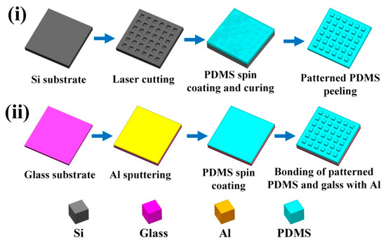
Figure 5.
Schematic of fabrication process for the bottom part of the VTENG.

Figure 6.
Optical images of the fabricated patterned PDMS with different microstructures: (a) Square micropillars, (b) circle micropillars, and (c) triangle micropillars.
The cantilever was 3D printed using polylactic acid (PLA). For the top part, the 0.2 μm Al was sputtered on a glass substrate with the thickness of 1 mm as both a positive triboelectric layer and top electrode. After fabrication of the cantilever and top parts, the two fabricated top parts (top part-1 and top part-2) were fixed on the tips of the main and secondary beams (Figure 1), respectively. Finally, the fabricated cantilever with two top parts and bottom parts were fixed to the vibration input source.
3. Testing and Discussion
3.1. Testing Setup
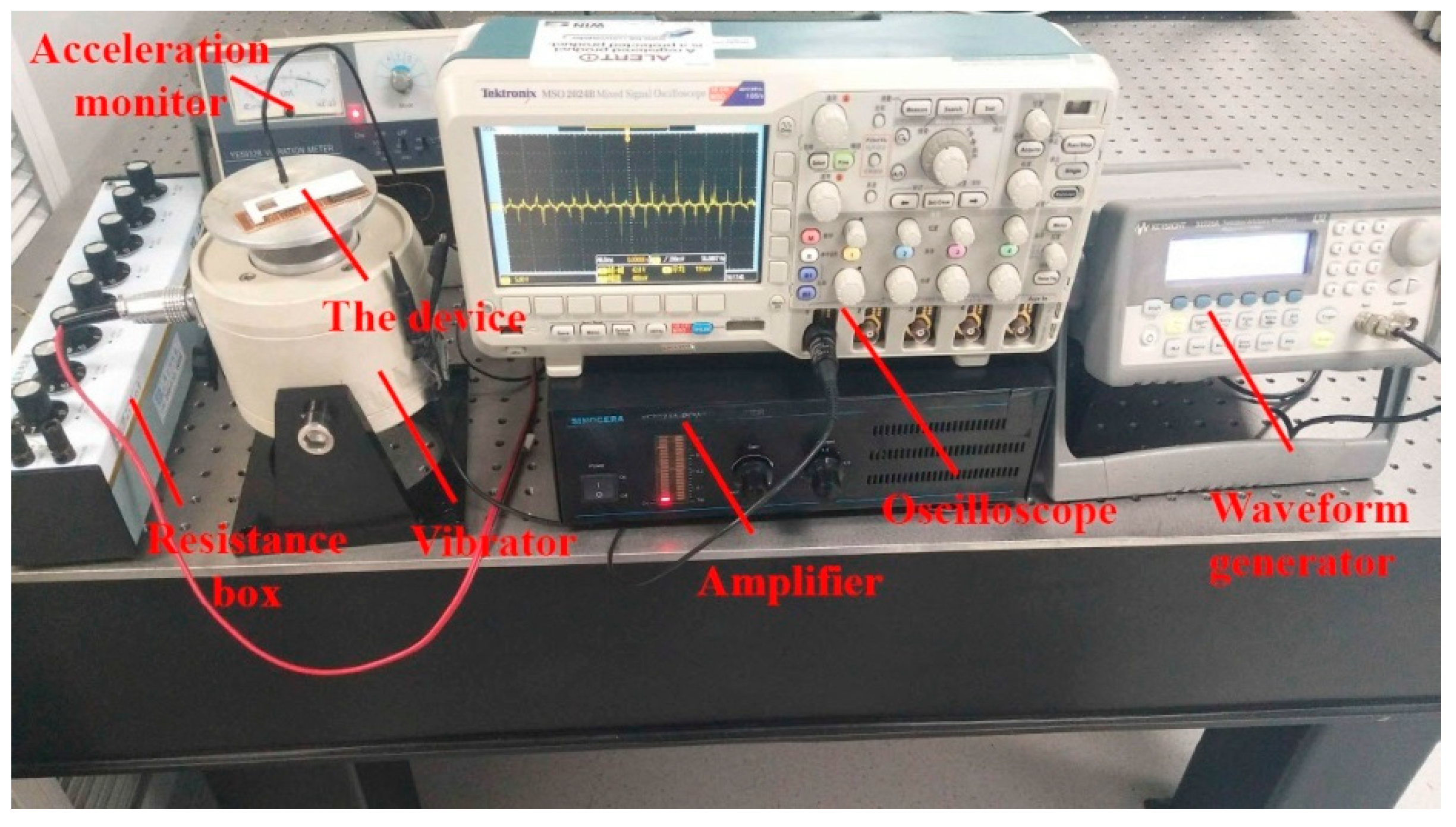
During the VTENG characteristic testing, a vibration testing system is assembled, as shown in Figure 7. It is comprised of a vibrator (JZK-5), waveform generator (33205A), power amplifier (YE5971A), acceleration monitor (YE5932B), resistance box (ZX99-1A), and oscilloscope (MDO3000). The fabricated device and the acceleration monitor are mounted on the vibrator. The waveform generator and power amplifier are used to control the vibration frequency and amplitude of the vibrator, and the acceleration of vibrator is monitored by the acceleration monitor. The resistance box is used to provide variable resistance to investigate the relationship between external resistance and output characteristic of the device. The electrical output of the device is recorded by an oscilloscope with the probe impedance of 100 MΩ.
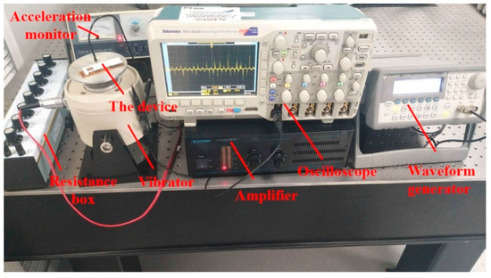
Figure 7.
Test system of the fabricated VTENG.
3.2. Tip Amplitudes of the VTENG without Bottom Parts Assembly
It is well known that gap distance between triboelectric layers is an important parameter that must be considered when assembling the device. Thus, the tip amplitudes from the main and secondary beams of the VTENG without bottom parts assembly were measured first. A laser micro-displacement measuring system (LTS-025-02) was used to evaluate the tip displacements of the main and secondary beams of the fabricated VTEHs versus the excitation frequency.
Figure 8 shows the measured tip amplitudes versus vibrating frequencies under different accelerations before the impact happens. The testing result indicates that the primary and secondary resonant frequencies of the VTENG are 23 Hz and 75 Hz, both of which are in the low-frequency range of less than 100 Hz. The measured resonant frequencies have small deviations from those obtained by FEM simulation and theoretical calculation, which is mainly caused by the cantilever fabrication process and the air damping effect. As mentioned above, the cantilever is 3D printed by using PLA and the material compactness of 3D printing affects the properties of the material, making the parameter settings inconsistent with the actual conditions in the FEM simulation. Therefore, the discrepancy can be effectively reduced by more accurately setting the simulated material parameters according to the actual situation in the following development.
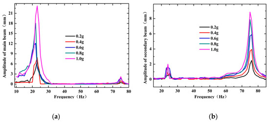
Figure 8.
Tip amplitudes at different accelerations: (a) The main beam and (b) secondary beam.
In addition, from Figure 8, tip amplitude from the main beam is much larger at the primary resonant frequency than that at the secondary resonant frequency, while tip amplitude of the secondary beam shows the opposite behavior. This means that the main TENG operates mainly around the primary resonant frequency, while the secondary TENG works mainly around the secondary resonant frequency. This result agrees well with the results of FEM simulation. As shown in Figure 8a, at the primary resonant frequency, the tip amplitude of the main TENG increases with vibration acceleration and when the vibration acceleration increases from 0.2 to 1.0 g, the tip amplitude is 7, 7.9, 12.1, 18.1, and 23.2 mm, respectively. At the secondary resonant frequency, the relationship between the tip amplitude of the secondary TENG and acceleration are similar to that of the main TENG at the primary resonant frequency, as demonstrated in Figure 8b. When the acceleration increases from 0.2 g to 1.0 g, the tip amplitude of the secondary TENG is 2.5, 3.9, 5.9, 7.9, and 8.8 mm, respectively. Therefore, according to the above-mentioned tip amplitude of the main and secondary beams, in order to ensure that the VTENG can work effectively around both the primary and secondary resonant frequencies for broadband operation under a low exciting acceleration level of 0.2 g, the gap distance between triboelectric layers when assembling the device should not exceed 2.5 mm.
3.3. Effect of Different PDMS Microstructures Configuration
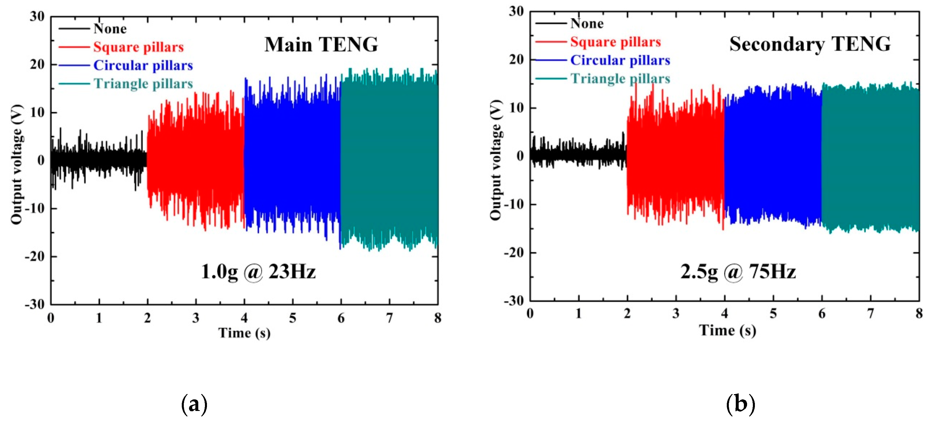
In order to study the output performance of the VTENG, the comparative characterization was performed on devices with four different PDMS microstructures in detail. Figure 9 shows the voltages of the main TENG and secondary TENG from the VTENGs with the following four different PDMS microstructures: none (no microstructure plane), square, circle, and triangle. The size of each of the single PDMS microstructures can be found in Figure 6. The result clearly demonstrates the order of the output performance of both the main and secondary TENGs of different VTENGs as none < square < circular <triangle. The dramatic increment in the output performance of the featured devices over the none-featured device is mainly caused by the increasing of effective triboelectrification and the resulting more surface charges. Meanwhile, the difference in output performance of the three featured devices may be due to the difference in capacitance change during the contact-separation process between triboelectric layers. The triangle-featured device has the largest area of air voids, followed by the circle-featured device. The existence of a larger area of air voids is beneficial to improve the effective dielectric constant, which results in an increase in the capacitance change during operation [40]. Moreover, as shown in Figure 9, when the excitation acceleration is 1 g, the maximum output voltage of the main TENG for triangle-featured device is up to 18.8 V at 23 Hz (the first resonant frequency of the VTENG), while the maximum peak output voltage of the secondary TENG is up to 14.9 V at 75 Hz (the secondary resonant frequency of the VTENG) under the excitation acceleration of 2.5 g; however, the main TENG and the secondary TENG for none-featured device can only produce the maximum peak voltages of 6.6 V and 5.0 V, respectively.
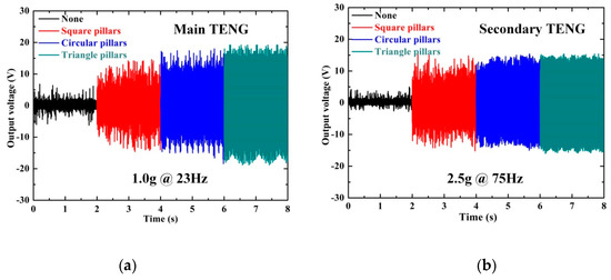
Figure 9.
Comparison of characterization of the VTENG with different microstructures: (a) Output voltage from the main TENG and (b) output voltage from the secondary TENG.
3.4. Broadband Behavior of VTENG
The broadband behavior of the device is evaluated by measuring output voltages of the main TENG excited at a frequency range around the first resonance frequency of 23 Hz and secondary TENG excited at a frequency range around the second resonant frequency of 75 Hz. As we can see in Figure 10a,b, when the acceleration increases from 0.3 g to 1.2 g in steps of 0.3 g, the peak output voltage of the main TENG around the first resonant frequency of 23 Hz is 5.3, 9.1, 15.9, and 20 V, while the peak output voltage from the secondary TENG around the second resonant frequency of 75 Hz is 2.9, 4.9, 6.5, and 7.8 V. The maximum output voltages of both the main and secondary TENGs increase with increasing vibration acceleration. The increased contact force between top and bottom parts is the reason behind this phenomenon. Higher contact force leads to the increased deformation of the PDMS, resulting in increased contact area between the triboelectric layers [34]. Meanwhile, it is noted that the output performance of the main TENG is significantly better than that of the secondary TENG. The larger output voltage (on 100 MΩ) of the main TENG can be attributed to the fact that both the amplitude and effective contact area of the main TENG are greater than those of the secondary TENG under the same acceleration conditions. The larger amplitude will result in a larger contact force when two triboelectric layers impact together, which will cause the effective contact area between triboelectric layers to increase [30]. Furthermore, the nonlinearity effect in the cantilever stiffness due to the contact between triboelectric layers is expected to increase the working bandwidth of the VTENG. Here, in order to judge the working broadband behavior of the VTENG, the full width at half maximum bandwidth is utilized. From Figure 10a,b, we can also observe that the operating bandwidth of the main TENG is increased from 3.5 Hz at 0.3 g to 15.1 Hz (around 23 Hz) at 1.2 g, while the operating bandwidth of the secondary TENG is increased from 3.1 Hz at 0.3 g to 12.5 Hz (around 75 Hz) at 1.2 g. The working bandwidths of both the main and secondary TENGs are increased with an increased vibration acceleration level. The reason is that a larger input vibration acceleration results in a larger amplitude of the cantilever and a corresponding impact effect between the triboelectric layers, thus providing a widening operable frequency range of the main and secondary TENGs [29].
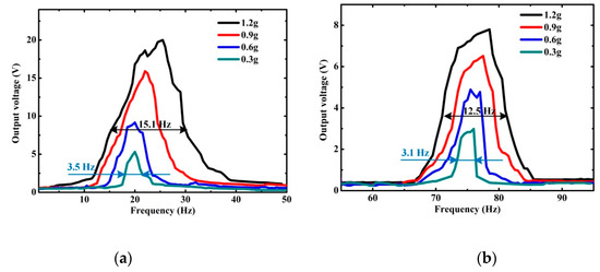
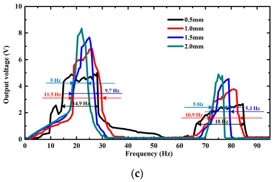
Figure 10.
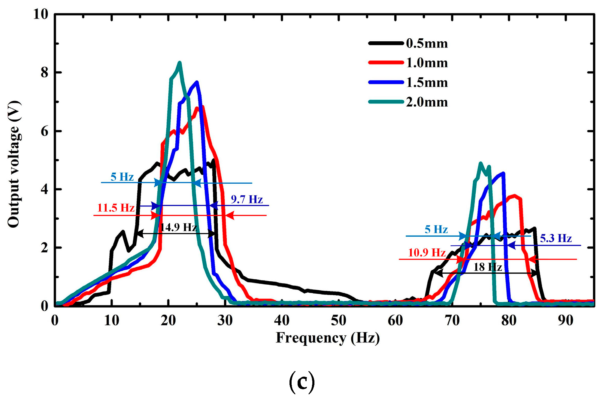
Frequency spectrums of the VTENG peak output voltage: (a) Main TENG peak voltage for different input vibration accelerations, (b) secondary TENG peak voltage for different vibration accelerations, and (c) the peak voltage of the device for different gaps at 0.6 g and 0.5 Hz to 95 Hz.
In order to study the influence of the gap distance on the output performance of the VTENG, corresponding experiments are conducted where both the main TENG and secondary TENG of the device are connected with the external circuit in a parallel manner. The results of changes in gap distance at 0.6 g and the frequency range of 0.5 Hz to 95 Hz are shown in Figure 10c. At around the primary resonant of 23 Hz, when the gap distance is 2.0, 1.5, 1.0, and 0.5 mm, the working bandwidth of the device is 5, 9.7, 11.5, and 14.9 Hz, respectively, while the corresponding maximum peak output voltage is 9.1, 7.7, 6, and 4.9 V, respectively. At around the secondary resonant of 75 Hz, as gap distance increases from 0.5 mm to 2.0 mm, the working bandwidth decreases from 18 Hz to 5 Hz, while the corresponding maximum peak output voltages increases from 2.7 V to 4.9 V. Thus, it is worth noting that the total operating bandwidth of the VTENG can reach up to 32.9 Hz at a low acceleration of 0.6 g (in the frequency range of less than 100 Hz) when the gap distance is 0.5 mm. The broadband performance of the device is listed and compared with other published TENGs in Table 2. This indicates that the operating bandwidth of our device has comparable performance. It is the integration of inherent nonlinearity caused by top and bottom parts impacting and nearby two resonant frequencies of the cantilever, that makes the VTENG capable of harvesting energy from a wide range of frequencies. Moreover, it can be concluded that the output voltage increases as the gap distance increases, but the operating bandwidth decreases. This is because a higher gap distance can increase the moving distance of the concentrated masses (i.e., top part-1 and top part-2 of VTENG), thereby increasing the impacting effect between top and bottom parts, resulting in a larger output voltage [31]. Meanwhile, as observed, the frequency around the primary and secondary resonant frequency at which highest voltage is obtained are shifted to the left when the gap distance increases.

Table 2.
Comparison among our device and other published TENGs with operating bandwidth.
3.5. Voltage and Power Characteristics
To investigate the electric power generation of the VTENG at the primary and secondary resonant frequencies of 23 Hz and 75 Hz, the main TENG and secondary TENG are connected to different external loads, then their output voltages are measured, and corresponding output powers are calculated at an acceleration of 1 g. Here, the output powers can be calculated by the following formula:
where Vpeak is the peak output voltage and R is the external resistance.
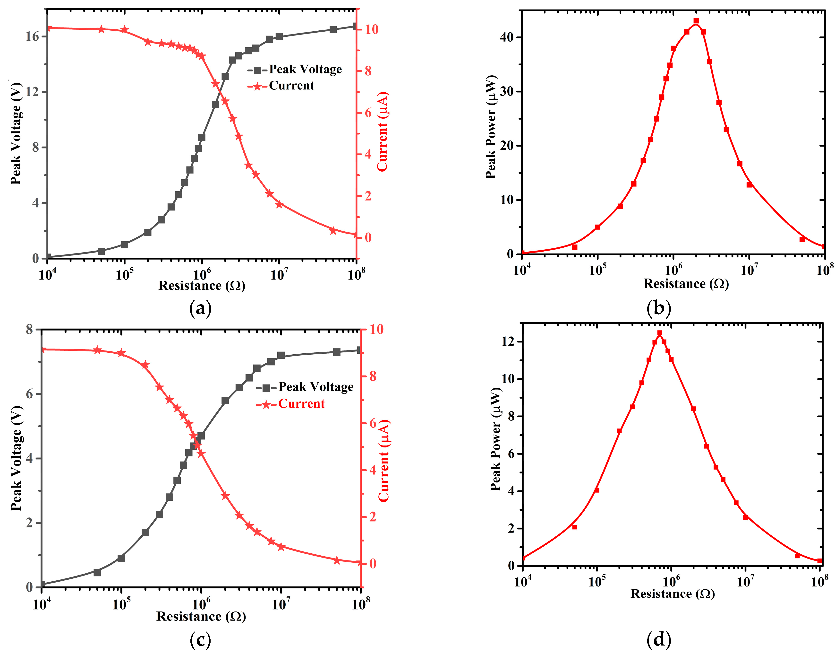
As illustrated in Figure 11a, the load voltage from the main TENG at the first resonant frequency gradually increases with increasing external load, while the current follows an opposite trend. The corresponding power output first increases until it reaches a peak of 43.08 μW at the optimal matched resistance of 2 MΩ, and then decreases (Figure 11b). At the condition of the optimal resistance, the peak voltage and current are 13.12 V and 6.56 μA, respectively. Meawhile, as the device works at the second resonant frequency, the relationship between the output voltages, current, and powers from the secondary TENG and the external loads are similar to those of the main TENG at the first resonant frequency, as demonstrated in Figure 11c,d. The secondary TENG has the instantaneous peak power of 12.5 μW at its optimal matched resistance of 0.7 MΩ, and the corresponding instantaneous voltage and current are 4.18 V and 5.97 μA, respectively. Furthermore, the areal power density can be defined as the output power of the main or secondary TENG divided by its effective area (the main TENG 4 cm2 and the secondary TENG 1 cm2), respectively. Thus, the maximum peak areal power densities of the main and secondary TENGs are 10.77 μW/cm2 and 12.5 μW/cm2, respectively. Both the power densities of the main and secondary TENGs are higher than many reported cantilevers based TENGs [29,31,34,42,43].
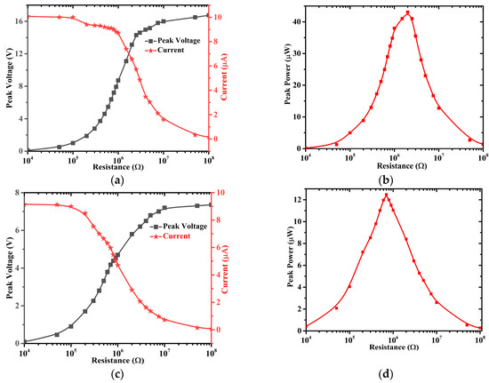
Figure 11.
VTENG output peak voltage, current, and power with resistances: (a) Output peak voltage and current and (b) instantaneous power from the main TENG at 23 Hz. (c) Output peak voltage and current and (d) instantaneous power with resistances from the secondary TENG at 75 Hz.
3.6. Capacitor Charging Characteristics
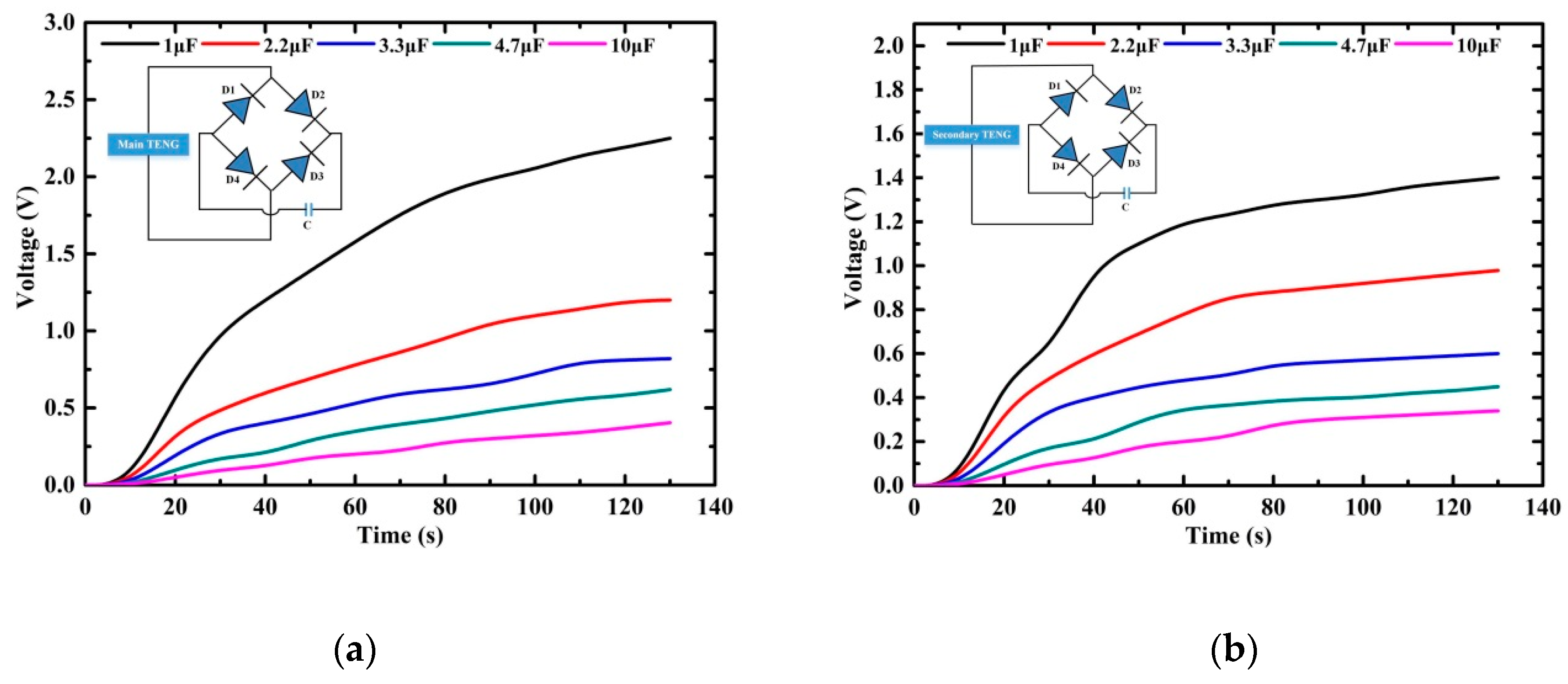
In practical applications, since TENG generates AC power and the power is too small to directly supply the load, a necessary step is needed to convert the AC output to DC power and store it in an energy storage unit such as a capacitor. To evidence this capability, the main TENG or secondary TENG with a rectifier and a capacitor are integrated into a circuit (see inset Figure 12a,b). For the main TENG, the electrical output measurement is carried out at 1 g and exciting frequency of 23 Hz (the primary resonant frequency), and the charging curves of capacitors with the capacitance of 1, 2.2, 3.3, 4.7, and 10 μF are illustrated in Figure 12a. The charged voltage for a 1 μF capacitor, can increase to 2.19 V within 120 s, while the voltage for a 10 μF capacitor only can reach up to 0.37 V within 120 s. For the secondary TENG, the electrical output measurement is carried out at 1 g and 75 Hz (the secondary resonant frequency of the device), and the charging curves with capacitors of 1, 2.2, 3.3, 4.7, and 10 μF are also depicted in Figure 12b. As mentioned above, the secondary TENG gives a smaller triboelectric contact area and vibration amplitude, and therefore a lower voltage output. Thus, under the same charging capacitor condition, the gradient of the charging curve from the secondary TENG is lower than the one from the main TENG. To the capacitor of 1 μF, the charged voltage of the secondary TENG can reach up to 1.38 V in about 120 s, while the charged voltage of 10μF capacitor only can be charged up to 0.33 V in about 120 s.
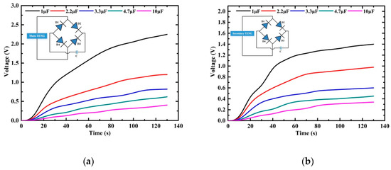
Figure 12.
The charging curves of various capacitors by the device: (a) The main TENG and (b) the secondary TENG. The inset is the circuit of the capacitor charging.
3.7. The Application of Fabricated VTENG
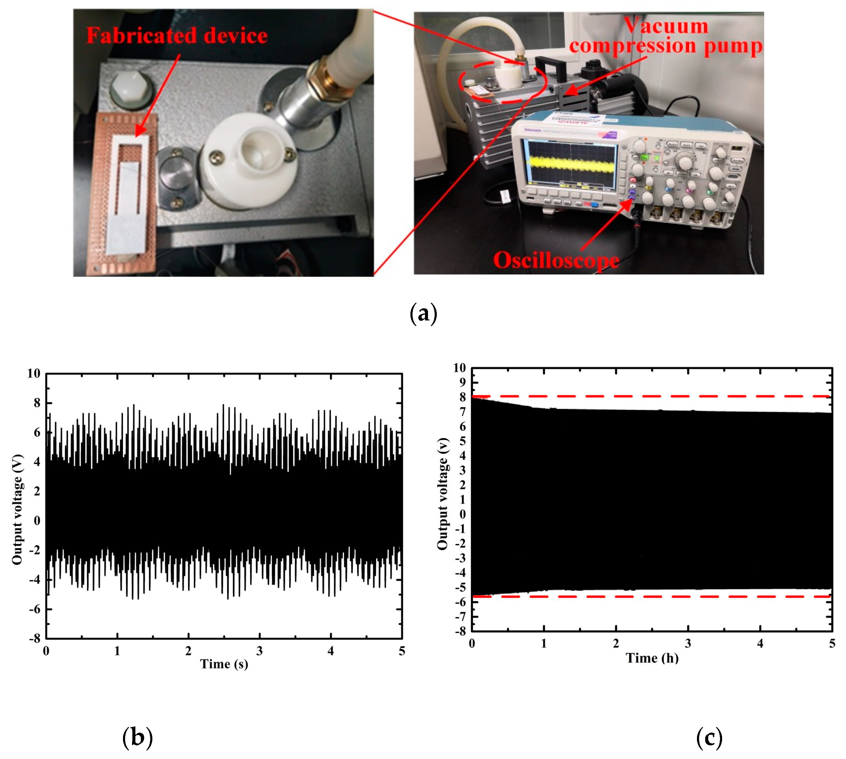
To verify the practical application capacity of the fabricated VTENG in daily life, the VTENG was tested on a vacuum compression pump. As shown in Figure 13a, the device is fixed on the vacuum compression pump and its output voltage is recorded by an oscilloscope. When the pump works, it vibrates and drives the device to oscillate. In this way, the oscillation causes the contact and separation between top and bottom parts of the device and enables the main TENG or secondary TENG to generate electrical voltage. According to the test results, the vibration frequency and acceleration of the pump are ~25 Hz and ~1.1 g, respectively, and thus the main TENG of the VTENG can work effectively under the vibration of the pump. The output voltage from the main TENG of the VTENG was recorded for 5 s (Figure 13b). The obtained maximum peak voltage from main TENG of the device was more than 8 V, which is basically consistent with the value depicted in Figure 10a. Meanwhile, to investigate the stability, the output voltage from main TENG of the VTENG is measured for 5 h under the vibration of the pump. The result shows that the output voltage of the device gradually decreases slightly during the first one hour (Figure 13c, but remains relatively stable during the last four hours. This may be because during the vibrating operation of the device, the stiffness and sizes of the PDMS microstructures initially change slightly due to impact between triboelectric layers, but then gradually stabilize. On the other hand, amid the rapid development of microelectronic circuits and micro and nano fabrication processes, a large number of low-power microelectronic devices have emerged. Their power consumption is very low, even on the order of μW with operating voltages of below 3 V in the inactive mode. This confirmed that this developed VTENG is capable of supplying power for some electronic devices with low-power consumption.
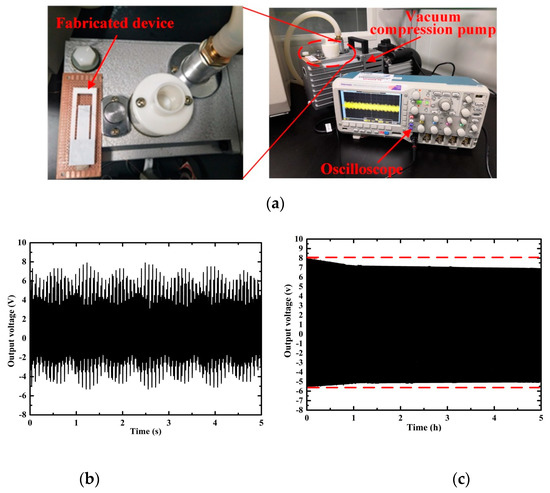
Figure 13.
The output performance of the device under an excitation vibration from a vacuum compression pump: (a) The testing setup, (b) the output voltage, and (c) the stability test.
4. Conclusions
In this work, the design, fabrication, and characterization of a 2DOF cantilever-based VTENG for low-frequency broadband operation have been demonstrated. The proposed 2DOF cantilever spring comprising one main beam and one inner secondary beam introduces multimode resonant behavior in the low-frequency range of less than 100 Hz which contributes to widening of bandwidth. With the help of combining multimode and inherent nonlinear characteristic due to the contact-separation triboelectric mechanism, the total operating bandwidth of the fabricated VTENG can reach up to 32.9 Hz at 0.6 g. The bandwidth of the device increases continuously as the vibration acceleration increases or the gap distance decreases.
The output performance of VTENG can increase by introducing microstructures on PDMS surface. Using scalable methods, four kinds of different PDMS microstructures are prepared. The output performance of the triangle-featured device performs best, far exceeding that exhibited by the none-featured films, and a maximum peak output voltage up to 18.8 V is obtained at the primary resonant frequency of 23 Hz under the input vibration acceleration of 1 g and 14.9 V at the secondary resonant frequency of 75 Hz under the input vibration acceleration of 2.5 g. Under the frequencies of these two modes at 1 g, the optimum peak power output of 43.08 μW and 12.5 μW from the main TENG and secondary TENG are obtained. It is also demonstrated that the capacitor charging ability can be driven by the main TENG and secondary TENG of the device. The main TENG can generate a charging voltage of 2.19 V and 0.37 V in 120 s for the 1 μF and 10 μF capacitors, respectively, while the secondary TENG can generate a charging of 1.38 V and 0.33 V, respectively. In addition, the fabricated device shows good stability with its voltage reaching and maintaining at 8 V when tested on a vacuum compression pump. The experimental results show that the proposed VTENG has the feasibility of powering electronic devices and systems with low-power consumption in wireless sensor networks.
Author Contributions
Conceptualization, G.T. and Q.S.; methodology, G.T. and F.C.; software, X.H.; validation, F.C. and B.H.; formal analysis, B.X. and Z.L.; investigation, G.T. and W.W.; data curation, F.C., X.H., B.H., and D.Y.; writing—original draft preparation, G.T. and F.C.; writing—review and editing, G.T., X.Y., Q.S., and W.W.; project administration, G.T., B.X., Z.L., X.Y., and D.Y.; funding acquisition, G.T., B.X., and X.Y.
Funding
This research was funded by the National Natural Science Foundation of China, grant number 51565038, and the Science and Technology Project of Jiangxi Provincial Education Department, grant number GJJ170986, GJJ151102, and GJJ180938.
Conflicts of Interest
The authors declare no conflict of interest.
References
- Wang, P.; Pan, L.; Wang, J.; Xu, M.; Dai, G.; Zou, H.; Dong, K.; Wang, Z.L. An ultra-low-friction triboelectric-electromagnetic hybrid nanogenerator for rotation energy harvesting and self-powered wind speed sensor. ACS Nano 2018, 12, 9433–9440. [Google Scholar] [CrossRef] [PubMed]
- Ud Din, A.; Kamran, M.; Mahmood, W.; Aurangzeb, K.; Saud Altamrah, A.; Lee, J. An efficient CMOS dual switch rectifier for piezoelectric energy-harvesting circuits. Electronics 2019, 8, 66. [Google Scholar] [CrossRef]
- Zhu, Y.; Yang, B.; Liu, J.; Wang, X.; Wang, L.; Chen, X.; Yang, C. A flexible and biocompatible triboelectric nanogenerator with tunable internal resistance for powering wearable devices. Sci. Rep. 2016, 6, 22233. [Google Scholar] [CrossRef] [PubMed]
- Khalili, M.; Biten, A.B.; Vishwakarma, G.; Ahmed, S.; Papagiannakis, A.T. Electromechanical characterization of a piezoelectric energy harvester. Appl. Energy 2019, 8, 113585. [Google Scholar] [CrossRef]
- Tang, G.; Liu, J.; Yang, B.; Luo, J.; Liu, H.; Li, Y.; Yang, C.; He, D.; Dao, V.D.; Tanaka, K.; et al. Fabrication and analysis of high-performance piezoelectric MEMS generators. J. Micromech. Microeng. 2012, 22, 065017. [Google Scholar] [CrossRef]
- Zhang, J.; Fang, Z.; Shu, C.; Zhang, J.; Zhang, Q.; Li, C. A rotational piezoelectric energy harvester for efficient wind energy harvesting. Sens. Actuators. A 2017, 262, 123–129. [Google Scholar] [CrossRef]
- Ju, S.; Ji, C. Impact-based piezoelectric vibration energy harvester. Appl. Energy 2018, 214, 139–151. [Google Scholar] [CrossRef]
- Zhang, Y.; Wang, T.; Wang, F.; Luo, A.; Hu, Y.; Li, X. Micro electrostatic energy harvester with both broad bandwidth and high normalized power density. Appl. Energy 2018, 212, 362–371. [Google Scholar] [CrossRef]
- Zhang, Y.; Wang, T.; Zhang, A.; Peng, Z.; Luo, D.; Chen, R.; Wang, F. Electrostatic energy harvesting device with dual resonant structure for wideband random vibration sources at low frequency. Rev. Sci. Instrum. 2016, 87, 125001. [Google Scholar] [CrossRef]
- Pan, Y.; Lin, T.; Qian, F.; Liu, C.; Yu, J.; Zuo, L.; Zuo, J. Modeling and field-test of a compact electromagnetic energy harvester for railroad transportation. Appl. Energy 2019, 247, 309–321. [Google Scholar] [CrossRef]
- Fan, K.; Cai, M.; Liu, H.; Zhang, Y. Capturing energy from ultra-low frequency vibrations and human motion through a monostable electromagnetic energy harvester. Energy 2019, 169, 356–368. [Google Scholar] [CrossRef]
- Ravichandran, A.N.; Calmes, C.; Serres, J.R.; Ramuz, M.; Blayac, S. Compact and high performance wind actuated venturi triboelectric energy harvester. Nano Energy 2019, 62, 449–457. [Google Scholar] [CrossRef]
- Lee, B.; Kim, D.H.; Park, J.; Park, K.; Lee, K.J.; Jeong, C.K. Modulation of surface physics and chemistry in triboelectric energy harvesting technologies. Sci. Technol. Adv. Mater. 2019, 20, 758–773. [Google Scholar] [CrossRef] [PubMed]
- Fu, Y.; Ouyang, H.; Davis, R.B. Triboelectric energy harvesting from the vibro-impact of three cantilevered beams. Mech. Syst. Sig. Process. 2019, 121, 509–531. [Google Scholar] [CrossRef]
- Cheng, T.; Li, Y.; Wang, Z.L.; Wang, Y.; Gao, Q.; Ma, T. Triboelectric nanogenerator by integrating a cam and a movable frame for ambient mechanical energy harvesting. Nano Energy 2019, 60, 137–143. [Google Scholar] [CrossRef]
- Xiao, X.; Zhang, X.; Wang, S.; Ouyang, H.; Chen, P.; Song, L.; Wang, Z.L. Honeycomb structure inspired triboelectric nanogenerator for highly effective vibration energy harvesting and self-powered engine condition monitoring. Adv. Energy Mater. 2019, 9, 1902460. [Google Scholar] [CrossRef]
- Sari, I.; Balkan, T.; Kulah, H. An electromagnetic micro power generator for wideband environmental vibrations. Sens. Actuators A 2008, 145–146, 405–413. [Google Scholar] [CrossRef]
- Liu, J.; Fang, H.; Xu, Z.; Mao, X.; Shen, X.; Chen, D.; Cai, B. A MEMS-based piezoelectric power generator array for vibration energy harvesting. Microelectron. J. 2008, 39, 802–806. [Google Scholar] [CrossRef]
- Qi, S.; Shuttleworth, R.; Olutunde Oyadiji, S.; Wright, J. Design of a multiresonant beam for broadband piezoelectric energy harvesting. Smart Mater. Struct. 2010, 19, 094009. [Google Scholar] [CrossRef]
- Ou, Q.; Chen, X.; Gutschmidt, S.; Wood, A.; Leigh, N. A two-mass cantilever beam model for vibration energy harvesting applications. In Proceedings of the 2010 IEEE International Conference on Automation Science and Engineering (CASE), Toronto, ON, Canada, 21–24 August 2010. [Google Scholar]
- Arafa, M.; Akl, W.; Aladwani, A.; Aldraihem, O.; Baz, A. Experimental implementation of a cantilevered piezoelectric energy harvester with a dynamic magnifier. Proc. SPIE 2011, 7977, 79770Q-1–79770Q-9. [Google Scholar] [CrossRef]
- Wu, H.; Tang, L.; Yang, Y.; Soh, C.K. A novel two-degrees-of-freedom piezoelectric energy harvester. J. Intell. Mater. Syst. Struct. 2012, 24, 357–368. [Google Scholar] [CrossRef]
- Kim, J.E.; Kim, Y.Y. Power enhancing by reversing mode sequence in tuned mass-spring unit attached vibration energy harvester. AIP Adv. 2013, 3, 72103. [Google Scholar] [CrossRef]
- Soliman, M.S.M.; Abdel-Rahman, E.M.; El-Saadany, E.F.; Mansour, R.R. A wideband vibration-based energy harvester. J. Micromech. Microeng. 2008, 18, 115021. [Google Scholar] [CrossRef]
- Liu, H.; Lee, C.; Kobayashi, T.; Tay, C.J.; Quan, C. Investigation of a MEMS piezoelectric energy harvester system with a frequency-widened-bandwidth mechanism introduced by mechanical stoppers. Smart Mater. Struct. 2012, 21, 035005. [Google Scholar] [CrossRef]
- Liu, H.; Tay, C.J.; Quan, C.; Kobayashi, T.; Lee, C. Piezoelectric MEMS energy harvester for low-frequency vibrations with wideband operation range and steadily increased output power. J. Microelectromech. Syst. 2011, 20, 1131–1142. [Google Scholar] [CrossRef]
- Zhu, J.; Wang, A.; Hu, H.; Zhu, H. Hybrid electromagnetic and triboelectric nanogenerators with multi-impact for wideband frequency energy harvesting. Energies 2017, 10, 2024. [Google Scholar] [CrossRef]
- Ibrahim, A.; Ramini, A.; Towfighian, S. Modeling an impact vibration harvester with triboelectric transduction. In Proceedings of the International Design Engineering Technical Conferences & Computers and Information in Engineering Conference IDETC/CIE, Cleveland, OH, USA, 6–9 August 2017. [Google Scholar]
- Bhatia, D.; Kim, S.W.; Kim, W.; Lee, S.; Choi, D. Tandem triboelectric nanogenerators for optimally scavenging mechanical energy with broadband vibration frequencies. Nano Energy 2017, 33, 515–521. [Google Scholar] [CrossRef]
- Yang, J.; Chen, J.; Yang, Y.; Zhang, H.; Yang, W.; Bai, P.; Wang, Z.L. Broadband vibrational energy harvesting based on a triboelectric nanogenerator. Adv. Energy Mater. 2014, 4, 1301322. [Google Scholar] [CrossRef]
- Ibrahim, A.; Ramini, A.; Towfighian, S. Experimental and theoretical investigation of an impact vibration harvester with triboelectric transduction. J. Sound Vib. 2018, 416, 111–124. [Google Scholar] [CrossRef]
- Nelson, D.; Ibrahim, A.; Towfighian, S. A tunable triboelectric wideband energy harvester. J. Intell. Mater. Syst. Struct. 2019, 30, 1745–1756. [Google Scholar] [CrossRef]
- Dhakar, L.; Tay, F.E.H.; Lee, C. Investigation of contact electrification based broadband energy harvesting mechanism using elastic PDMS microstructures. J. Micromech. Microeng. 2014, 24, 104002. [Google Scholar] [CrossRef]
- Dhakar, L.; Tay, F.E.H.; Lee, C. Development of a broadband triboelectric energy harvester with SU-8 micropillars. J. Microelectromech. Syst. 2014, 24, 91–99. [Google Scholar] [CrossRef]
- Nafari, A.; Sodano, H.A. Surface morphology effects in a vibration based triboelectric energy harvester. Smart Mater. Struct. 2017, 27, 015029. [Google Scholar] [CrossRef]
- Niu, S.; Wang, S.; Lin, L.; Liu, Y.; Zhou, Y.S.; Hu, Y.; Wang, Z.L. Theoretical study of contact-mode triboelectric nanogenerators as an effective power source. Energy Environ. Sci. 2013, 6, 3576–3583. [Google Scholar] [CrossRef]
- Xu, G.; Li, X.; Xia, X.; Fu, J.; Ding, W.; Zi, Y. On the force and energy conversion in triboelectric nanogenerators. Nano Energy 2019, 59, 154–161. [Google Scholar] [CrossRef]
- Zayed, A.A.A.; Assal, S.F.M.; Nakano, k.; Kaizuka, T.; EI-Bab, A.M.R.F. Design procedure and experimental verification of a broadband quad-stable 2-DOF vibration energy harvester. Sensors 2019, 19, 2893. [Google Scholar] [CrossRef]
- Wu, H.; Tang, L.; Yang, Y.; Soh, C.K. Development of a broadband nonlinear two-degree-of-freedom piezoelectric energy harvester. J. Intell. Mater. Syst. Struct. 2014, 25, 1875–1889. [Google Scholar] [CrossRef]
- Fan, F.; Lin, L.; Zhu, G.; Wu, W.; Zhang, R.; Wang, Z.L. Transparent triboelectric nanogenerators and self-powered pressure sensors based on micropatterned plastic films. Nano Lett. 2012, 12, 3109–3114. [Google Scholar] [CrossRef]
- Jeon, S.; Kim, D.; Seol, M.; Park, S.; Choi, Y. 3-Dimensional broadband energy harvester based on internal hydrodynamic oscillation with a package structure. Nano Energy 2015, 17, 82–90. [Google Scholar] [CrossRef]
- Quan, T.; Yang, Y. Fully enclosed hybrid electromagnetic–triboelectric nanogenerator to scavenge vibrational energy. Nano Res. 2016, 9, 2226–2233. [Google Scholar] [CrossRef]
- Yang, W.; Chen, J.; Zhu, G.; Wen, X.; Bai, P.; Su, Y.; Wang, Z.L. Harvesting vibration energy by a triple-cantilever based triboelectric nanogenerator. Nano Res. 2013, 6, 880–886. [Google Scholar] [CrossRef]
© 2019 by the authors. Licensee MDPI, Basel, Switzerland. This article is an open access article distributed under the terms and conditions of the Creative Commons Attribution (CC BY) license (http://creativecommons.org/licenses/by/4.0/).

