Article

A 3GSps 12-bit Four-Channel Time-Interleaved Pipelined ADC in 40 nm CMOS Process

1
Institute of Microelectronics of the Chinese Academy of Sciences, Beijing 100029, China
2
School of Microelectronics, University of Chinese Academy of Sciences, Beijing 100049, China
*
Author to whom correspondence should be addressed.
Electronics 2019, 8(12), 1551; https://doi.org/10.3390/electronics8121551
Submission received: 12 November 2019 / Revised: 9 December 2019 / Accepted: 11 December 2019 / Published: 16 December 2019
(This article belongs to the Section Circuit and Signal Processing)

Abstract

:
This paper presents a four-channel time-interleaved 3GSps 12-bit pipelined analog-to-digital converter (ADC). The combination of master clock sampling and delay-adjusting is adopted to remove the time skew due to channel mismatches. An early comparison scheme is used to minimize the non-overlapping time, where a custom-designed latch is developed to replace the typical non-overlapping clock generator. By using the dither capacitor to generate an equivalent direct current input, a zero-input-based calibration is developed to correct the capacitor mismatch and inter-stage gain error. Fabricated in a 40 nm CMOS process, the ADC achieves a signal-to-noise-and-distortion ratio (SNDR) of 57.8 dB and a spurious free dynamic range (SFDR) of 72 dB with a 23 MHz input tone. It can achieve an SNDR above 52.3 dB and an SFDR above 61.5 dB across the entire first Nyquist zone. The differential and integral nonlinearities are −0.93/+0.73 least significant bit (LSB) and −2.8/+4.3 LSB, respectively. The ADC consumes 450 mW powered at 1.8V, occupies an active area of 3 mm × 1.3 mm. The calculated Walden figure of merit reaches 0.44 pJ/step.

1. Introduction

Direct sampling receivers [1,2,3,4] are playing more critical roles in modern 5G communication base stations, where traditional downconverter parts, such as mixers, local oscillator, intermediate frequency (IF) amplifiers and anti-aliasing filters, are replaced with radio-frequency analog-to-digital converters (RF-ADCs). This direct sampling scheme brings in several benefits. First, the alias frequency bands can be spaced much far away from the frequency band of interest and hence mitigating the design difficulty of the filters. Second, the non-idealities of downconversion components like local oscillator leakage in traditional IF architecture could produce an unwanted emission within the desired transmission, hence degrading system performance. With the direct sampling scheme, the system signal-to-noise-and-distortion ratio (SNDR) can be optimized because the downconversion components are removed from the critical signal path. Third, the high data throughput of 5G communication lies in the introduction of multiple-input, multiple-output (MIMO) antenna technology on a massive scale. The direct sampling scheme not only minimizes the size, heat and complexity in massive MIMO systems but also reduces the overall cost by saving the on board components. However, the performance bottleneck in a direct sampling receiver is the RF-ADC. Previous studies have proven that the direct sampling RF-ADCs are required to have both high resolution (>10-bit) and fast conversion speed (>1GSps) [5,6,7,8]. Particularly, 3GSps 12-bit pipelined ADC has become a good choice due to its economy and practicality for the 5G communication. For such high conversion speed, time-interleaving structure has become the mainstream architecture to keep the ADC in the linear power-speed region [9,10,11,12,13,14,15,16,17].
For interleaving ADCs, the matching impairments such as gain-mismatch, offset-mismatch and time skew could significantly deteriorate their performance. The gain and offset mismatches have been addressed in previous studies using digital calibration [17,18]. Although many techniques have been developed to overcome the time skew issue, they usually need auxiliary circuits such as extra channels [12,16], digital multipliers [10,12,13,14] and long finite impulse response (FIR) filters [11,15], which could not only degrade the performance of the ADC but also consume plenty of power. For the pipeline stages in the single channel, a proper clock scheme could significantly relax the circuit design. In the conventional comparison scheme, the sub-ADC makes its decision in the non-overlapping time, which not only claims a high requirement for the comparator but also squeezes the settling time of the residue amplifier (RA) [19]. In addition, the dynamic performance of the pipelined ADC is also limited by the linearity error in the pipeline stages, such as the inter-stage gain error and the capacitor mismatch [18,20,21]. These errors are usually corrected by digital calibration [20,21,22,23,24]. In traditional calibration methods, an additional driving circuit is usually needed to provide a specific input voltage, which may suffer from accuracy, frequency and power efficiency deterioration [18,25].
To address these issues, this paper designed a 3GSps 12-bit time-interleaving pipelined ADC with 0.5-bit redundancy multiplying digital-to-analog converter (MDAC), where several techniques have been exploited. First, a master clock sampling (retiming) scheme combined with a delay-adjusting variable delay line (VDL) is designed to remove the time skew, avoiding a massive capacitor array. Second, an early comparison scheme [26] is utilized to allocate the sub-ADC an approximate quarter of the clock cycle for resolving the digital code. Thus the non-overlapping, that doesn’t contain the sub-ADC resolving time, is minimized to allow more settling time for RA. Moreover, a custom-designed latch is developed to generate the non-overlapping clock, which simplifies the circuit design, reduces the clock jitter and saves the power consumption as well as the die area. Third, a zero-input-based calibration is developed to correct the linearity error, which avoids the extra driving circuits to achieve both high conversion speed and good linearity. In this calibration, the actual bit-weight of every digital-to-analog converter (DAC) capacitors in the first three MDACs is measured with an equivalent direct current (DC) input instead of the real input voltage.
The multi-GSps ADC also benefits from advanced process for two reasons. First, the sampling switch is a critical component for multi-GS/s ADC which turns on and off the capacitors for signal sampling and charge transfer. With the advanced process, it can achieve the faster rising and fall time characteristics for quickly switching between the sample and hold phases and a low RC (low on-resistance and small stray capacitance) time constant to make the switched capacitor circuit charge and discharge faster. Second, the advanced process offers the high trans-conductance transistors with low parasitic capacitance as the RA input devices which are optimal for the wide bandwidth and the good phase margin. However, a high-gain RA design is more and more difficult as the process scales down due to the decreased intrinsic gain of transistor. The 40 nm CMOS process is adopted to implement this ADC owing to its small stray capacitance and appropriate intrinsic gain of the transistor, where both the sampling switch and the RA requirements can be fulfilled with a reasonable effort.

2. Proposed ADC Architecture

Figure 1 shows the block diagram of the designed four-channel time-interleaved ADC. The 3 GHz input clock is divided by 4 to generate four clocks of 750 MHz with different phases (ph0~ph3), and three adjacent of phases are fed into the channel clock generator to produce their inner-clocks with the retiming clock Φ <k> (digitally controlled by a 4 bits VDL). In each channel, the sampling clocks (clks1 and clksc) for the first MDAC stage are retimed by the sampling latch (SL) that is driven by Φ <k> to overcome the time skew between the interleaved channels. The digital code for controlling Φ <k> is given by a background calibration [9] that is performed digitally by observing the ADC output without a separate timing reference channel. To align with the sampling clock, the other inner clocks such as non-overlapping clocks (clks and clkf) and comparator clock (clkc) are also retimed with the same clock. Due to the minimized non-overlapping time, the deliberated non-overlapping clock generator (NCG) is dispensable so that a custom-designed latch for non-overlapping clock (CLNC) is developed to generate the clks and clkf.
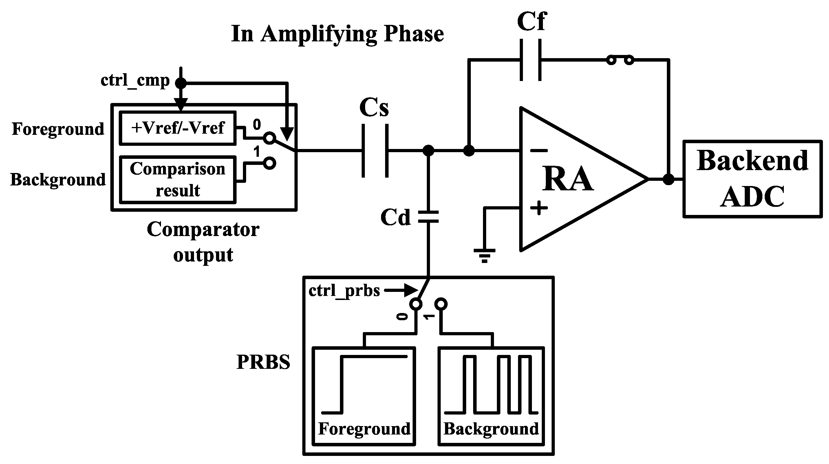
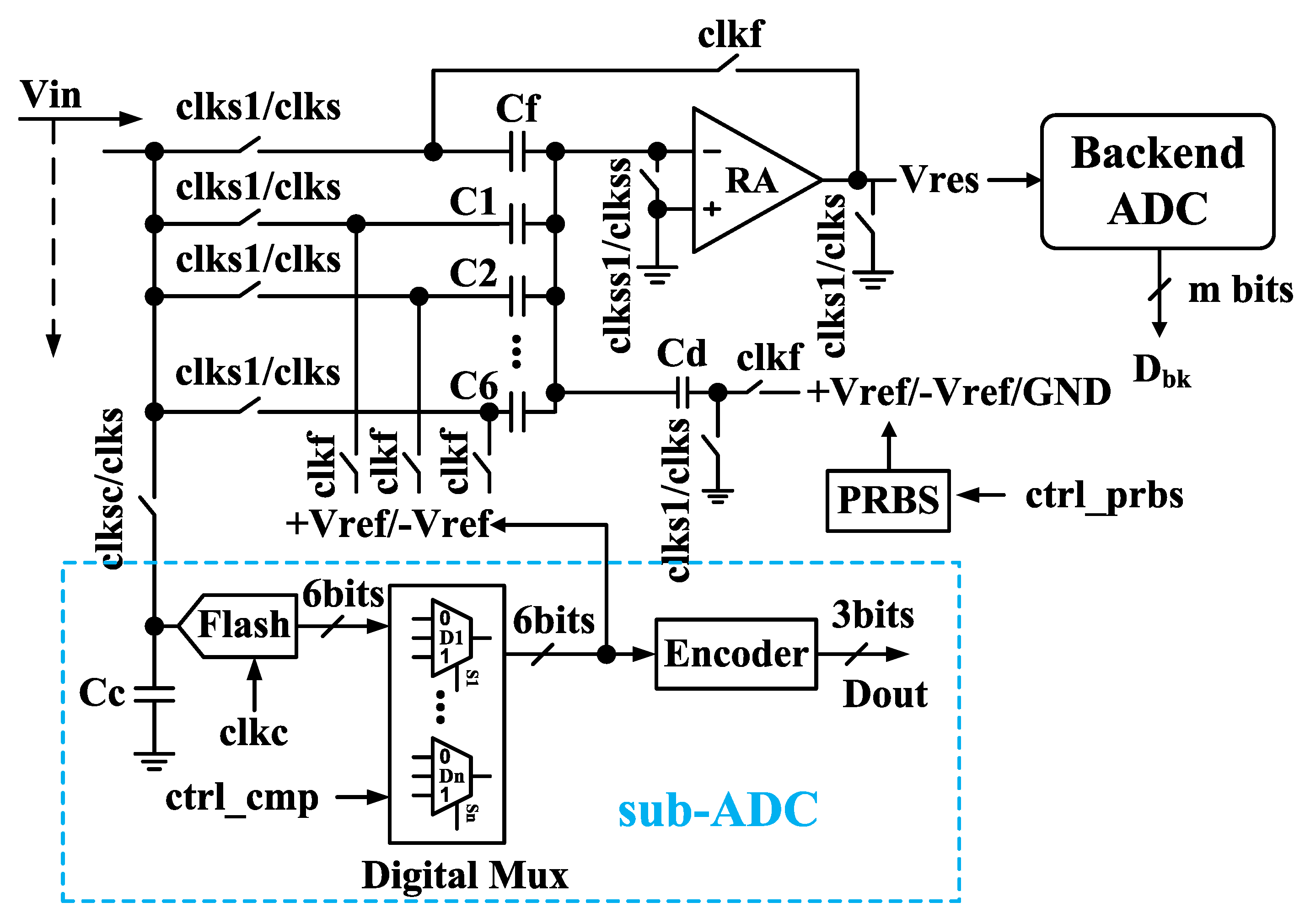
Sample and hold amplifier less (SHA-less) front end is utilized for each channel. And the resulting aperture error is removed by a VDL in Figure 1. Every channel consists of five 2.5-bit MDACs with 0.5-bit redundancy followed by a 2-bit flash. In the first three MDAC stages, both foreground and background calibrations are applied by sending commands to the control block via the SPI bus. According to the commands, the control block sends control signals (ctrl_prbs and ctrl_cmp) to the pseudorandom bit sequence (PRBS) circuits and the comparators in the sub-ADC as illustrated in Figure 2. The PRBS circuit has two operation modes. In the foreground calibration, it sends a constant signal to the dither capacitor Cd in the amplifying phase so that a fixed charge injection is created on the input stored on the switch capacitors. Cooperated with the outputs of comparators controlled by the signal ctrl_cmp, the bit-weight is measured to correct the linearity error. In the background calibration, a pseudo-random signal is sent by the PRBS circuit which is uncorrelated with the input signal. The dither is injected into residue voltage. Through the accumulation and average, the inter-stage gain error is corrected by the correlation-based calibration [19].

3. Circuits Implementation and Calibration

3.1. The Combination of Retiming and Delay-Adjusting

Figure 3a shows the ideal timing diagram for master clock sampling. The ph0~ph3 are the divided clocks in Figure 1. They suffer from the time skew caused by the different signal path and the variation in the delay gates, which results in the different phase shifts between two adjacent of clocks, as shown in Figure 3a. Therefore, ph0~ph3 are not directly used as the sampling clocks. The master clock sampling is a widely used technique [7,27] to reduce the time skew. CK M C is the master clock that has a sufficiently low clock jitter to drive each clock block on the chip. The sampling clocks (ch0_clks1~ch3_clks1) are retimed with the CK M C . Theoretically, the sampling clocks should have been optimally aligned with the rising edges of the master clock. Nevertheless the achievable sampling skew is usually limited to several hundreds of femtosecond (RMS) due to the layout parasitics associated with the sampling clocks and the mismatches of related devices. The delay-adjusting is a general technique that deals with the time skew for the time-interleaved ADC with high resolution [28] or ultra-high sampling rate [12]. However it usually takes a massive capacitor array (≥7 bits) to achieve both wide correction range and small step size.
Figure 3b presents the retiming scheme combined with delay-adjusting used in this paper. CK 3 G is the master clock of 3GHz for this time-interleaved ADC. The sampling clock for each channel is retimed by the SL with CK 3 G . And four VDLs are located in the master clock (CK 3 G ) path to further correct the delay mismatch. In the layout, the VDL and SL are placed as close as possible to the sampling switches to reduce the path mismatch. Furthermore, they are also optimized by appropriate transistor size to decrease the gate delay mismatch. The retiming scheme provides a coarse-tuning of the delay mismatch that compresses the correction range for the fine-tuning. It saves the most-significant-bit (MSB) capacitors of the programmable delay line in References [12,28].
The fine-tuning is provided by the VDLs consisting of a 4 bits digitally controlled capacitor array and the CMOS inverters as shown in Figure 3b. The unit capacitor is 0.4fF, which achieves the step size of 0.15ps. The digital calibration in Reference [9] is adopted to detect the mismatch caused by time skew. The channel ch0 serves as the timing reference. The sampling instants of other channels (t1’~t3’) are offset from their ideal values (t1~t3) as shown in Figure 4a. First, five adjacent sampled points (x0~x4) are given by the four channels (ch0~ch3). Among of them, x1~x3 are sampled by the calibrated channels ch1~ch3, respectively. x0 and x4 are sampled by the reference channel ch0. Second, the ch0 and ch2 are considered as an independent sampling system with half of the full sampling rate. Therefore the timing mismatch Δ T2 between ch0 and ch2 can be detected by evaluating the average value of |x2-x0|-|x4-x2| as shown in Figure 4b. With the detection results, the digital code is produced to feed into the VDL of the ch2 for tuning the sampling instant. Third, when the sampling instant of ch2 is tuned to its ideal value, the average values of |x1-x0|-|x2-x1| (shown in Figure 4c) and |x3-x2|-|x4-x3| (shown in Figure 4d) are simultaneously evaluated to detect the timing mismatch Δ T1 and Δ T3. Then they are removed by the VDLs in the ch1 and ch3. Although only three of the VDLs are employed during the calibration, the forth VDL is necessary to guarantee the performance of master clock sampling. Moreover, any one of four channels can be the timing reference with four VDLs.

3.2. Early Comparison Scheme

The operation of sub-ADC is usually performed in the non-overlapping time [19]. But the long non-overlapping time results in a short settling time for the RA. When the sub-ADC takes 10% of unit conversion period (UCP) to make its decision, just about 35% of UCP is left for the RA output to settle to the needed accuracy [19]. With this clock scheme, the blocks with high power consumption are needed to achieve high conversion speed, such as the high-speed comparators and the RA with high gain-bandwidth product [18,19]. The early comparison scheme [26] is adopted to relax the speed requirement for both comparators and RA, saving the power consumption.
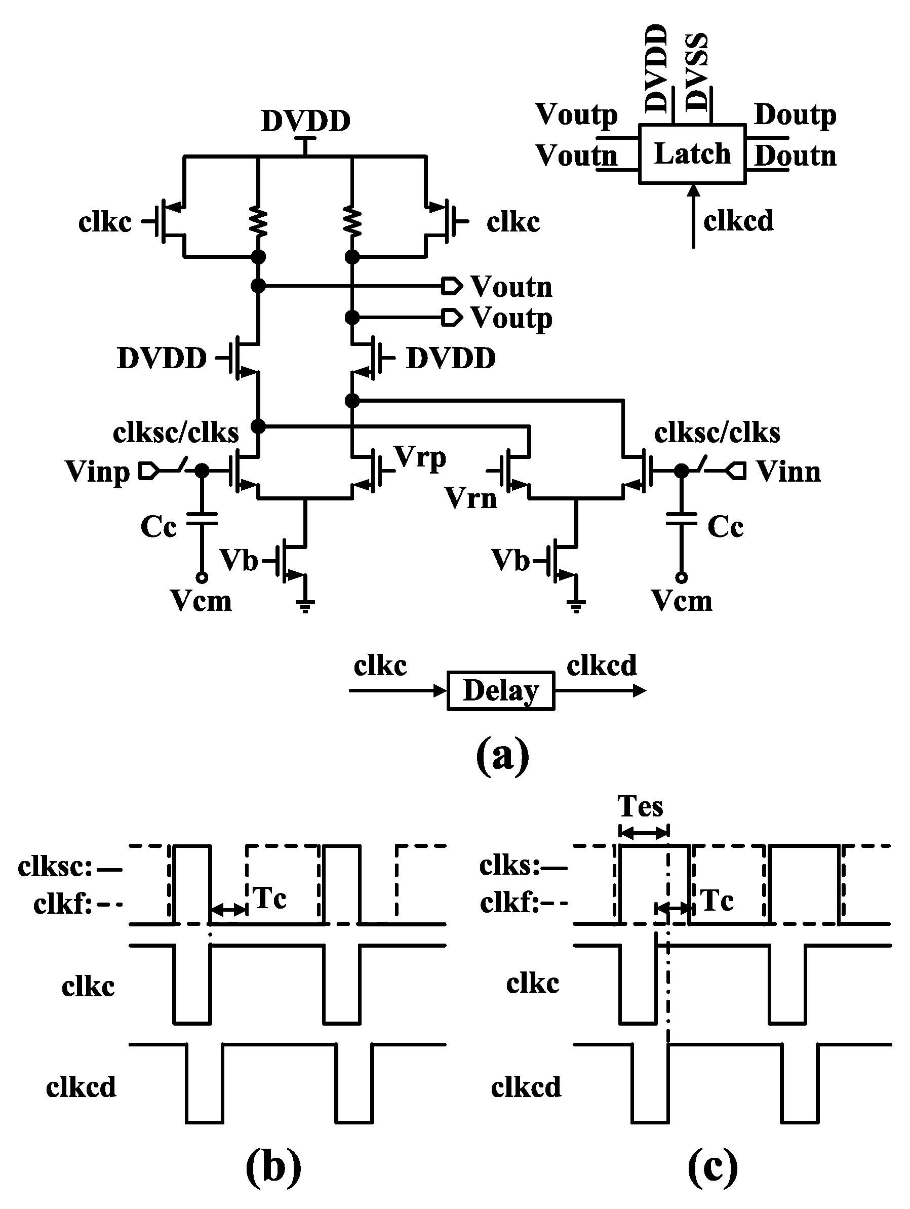
To implement the early comparison scheme, the comparator used in sub-ADC is shown in Figure 5a. For a 2.5-bit MDAC, the comparator offset of just 75 mV can be tolerated due to the full scale of 1.2 V. In the typical dynamic cross-coupled latch [29], process variation and device mismatches bring about a large offset voltage. Therefore the preamplifier is designed to reduce the offset voltage and isolate the kick-back noise, where the two nMOS pairs are connected to the input and reference as shown in Figure 5a. The clksc/clks are the sampling clocks for the 1st stage and the rest stages, respectively. When the rising edge of clkc arrives, the comparison result of the input sampled on the capacitor Cc and the reference starts to be amplified onto the nodes Voutp/Voutn. While the rising edge of clkcd delayed by the clkc arrives, the latch is enabled to start regenerating the output (Doutp/Doutn). Then the quantization result is propagated through the driving circuits and the digital mux to the MDAC before the rising edge of clkf. Figure 5b shows the timing diagram for the 1st stage, the duty cycle of the sampling clock (clksc) is 25% in virtue of the four-channel time-interleaving. Naturally, the sub-ADC starts to work as soon as the sampling phase is finished. It has 20% above of UCP to make the decision. And about 45% of UCP is left for the RA to settle to the desired accuracy. For the rest stages, the duty cycle of the sampling clock (clks) changes to 45% as shown in Figure 5c. However the clkc/clkcd are applied as the same as the 1st stage. In other words, the sub-ADC starts to work in the middle of the sampling phase. The effective sampling time for the sub-ADC becomes as shown in Figure 5c, which leads to a lower resolution for the effective signal sampled on the sub-ADC compared to the MDAC. But the difference between the two sampling paths is small and constant, which is equivalent to a comparator offset that can be corrected by the redundancy. With the early comparison scheme for the comparator discussed above, 20% above of UCP (Tc as shown in Figure 5b,c) is allocated for the sub-ADC and about 45% of UCP is for RA. The non-overlapping time is reduced to less than 10% of UCP.
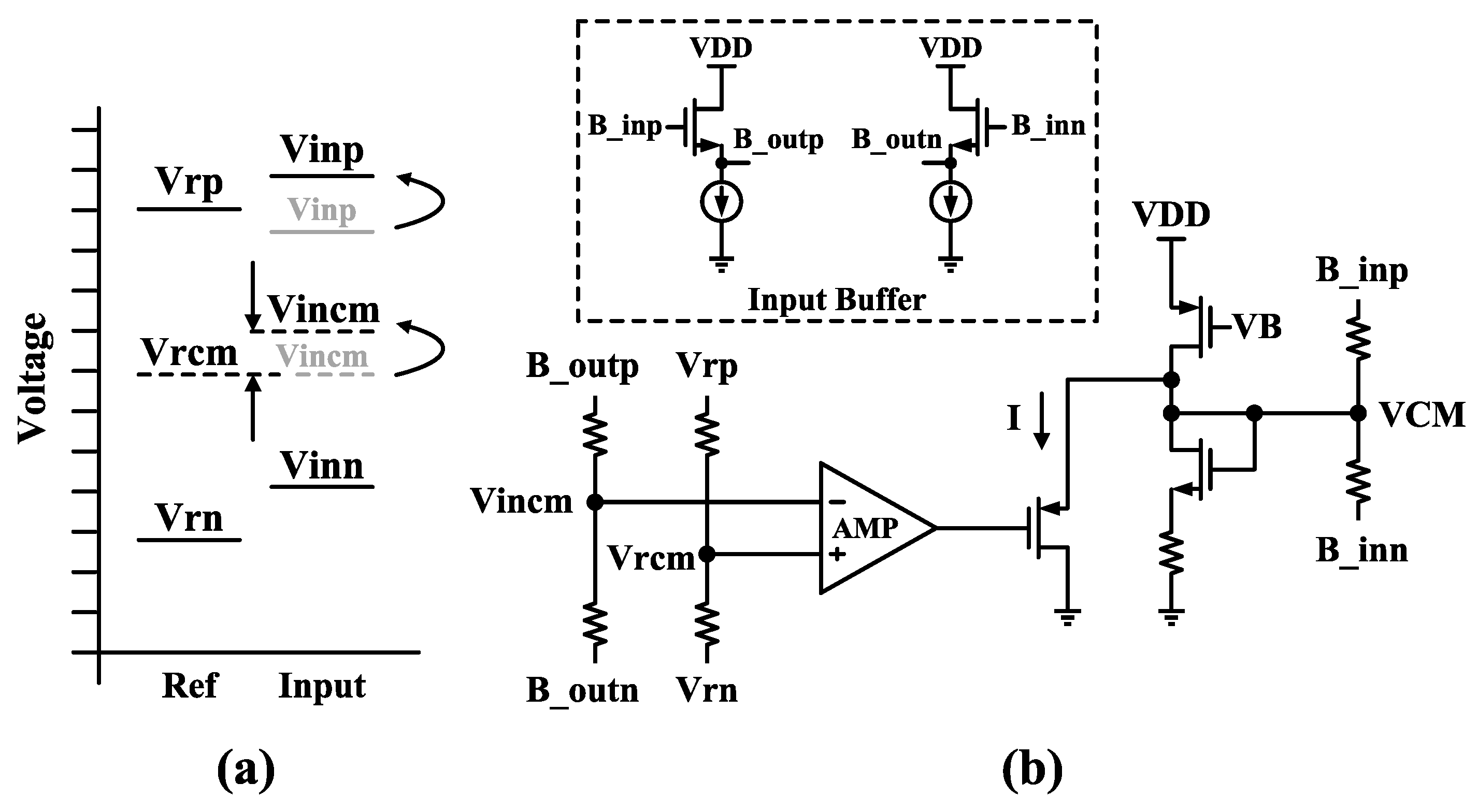
The offset voltage due to the mismatch in latch is minimized by the preamplifier. However the offset voltage, caused by the common-mode mismatch between the input and reference, is also non-negligible [26]. When the common-modes of the input and reference (Vincm and Vrcm as shown in Figure 6a are aligned, the (Vinp-Vrp) and (Vrn-Vinn) have the same polarity on the output of the preamplifier. As the common-mode mismatch appears, the polarity would become opposite with the approaching of the input to the reference. Coupled with the device mismatches in the preamplifier, the comparator offset would get worse. A feedback circuit is presented in the Figure 6b to remove the common-mode mismatch in the 1st MDAC stage. B_outp and B_outn are the outputs of the input buffer connected to the inputs of the sub-ADC. They follow the input signal B_inp and B_inn. The common-mode is obtained by an amplifier with two identical resistances. The difference of two common-modes is amplified into a trans-impedance circuit, which controls the common-mode of B_inp and B_inn. The common-mode mismatch between the input of sub-ADC and the reference is removed by the feedback circuit so that the corresponding comparator offset is canceled. And little power consumption is needed due to the slow change of common-mode. The common-mode mismatches for the rest stages are addressed by the strong common-mode feedback circuits of the residue amplifiers in their preceding stages.

3.3. The Implementation of CLNC

The typical NCG is usually implemented by cascading several logic gates and clock buffers [18], which adjusts the non-overlapping time in a wide range. However its power consumption and area increase dramatically along with the required clock speed.
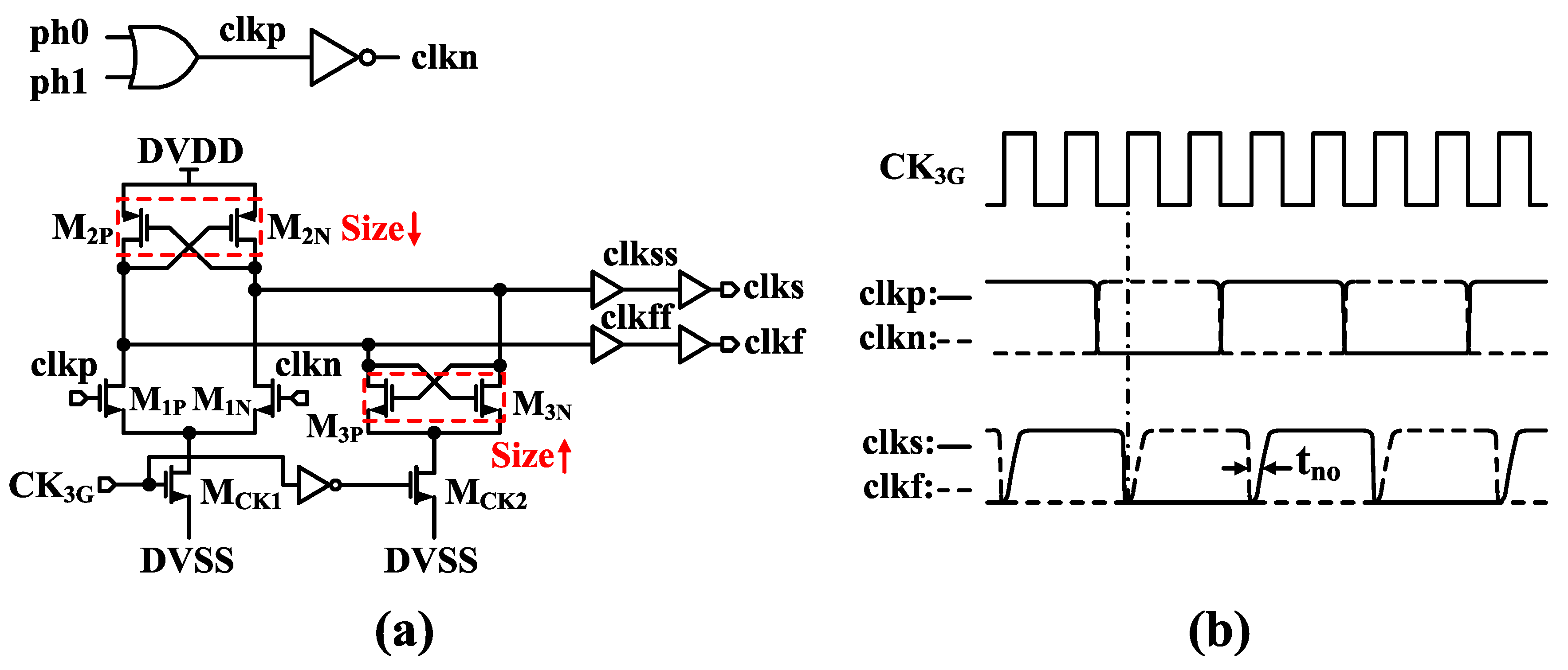
Owing to the minimized non-overlapping time, the typical NCG is replaced by a CLNC as shown in Figure 7a. It takes the clocks clkp/clkn as the input which are generated by two adjacent of phases (ph0 and ph1 etc.) via an OR logic gate and an inverter. When the clkp is low (clkn is high), a rising edge of CK 3 G triggers the rising edges of clkf as shown in Figure 7b and clkff which enable the amplifying phase of all the odd stages, as well as the sampling phase of all the even stages. And they operate in the opposite phase when the complementary clock is triggered (the sampling phase of the 1st stage is enabled by clks1 and clkss1). The non-overlapping time between the two phases is required to minimize the effects of signal-dependent charge injection which depends on the design of two cross-coupled nMOS and pMOS pairs as shown in Figure 7a. It is noticed that the rising edge of the retimed clock is determined by the pMOS pair (M 2 P /M 2 N ) while the falling edge is determined by the nMOS pair (M 3 P /M 3 N ). For generating the non-overlapping clock, the asymmetrical edges are required for the rising and falling on the premise that the sampling performance doesn’t degrade. The sampling resolution is mostly determined by the falling edge which can reduce the distortion with a short settling time. Therefore the M 3 P /M 3 N are designed with large size for the sharp edge. Meanwhile, the M 2 P /M 2 N are designed with relative small size to flatten the rising edge for producing the non-overlapping time (t n o ), as shown in Figure 7b. The combination of typical NCG and master clock sampling is realized by the CLNC. The total clock jitter is improved because of less transistors compared to the typical NCG. Moreover, the merging of NCG into latch also saves the power consumption and die area.

3.4. Zero-input-based calibration

Compared with the 1-bit redundancy MDAC, the 0.5-bit can save one comparator per stage and avoid the offset of ADC output [30]. Therefore, the 0.5-bit redundancy MDAC as shown in Figure 8 is employed in the pipelined ADC of this paper. To avoid the additional driving circuits in the calibration for 0.5-bit redundancy, this paper developed a zero-input-based foreground calibration with an improved bit-weight measurement.
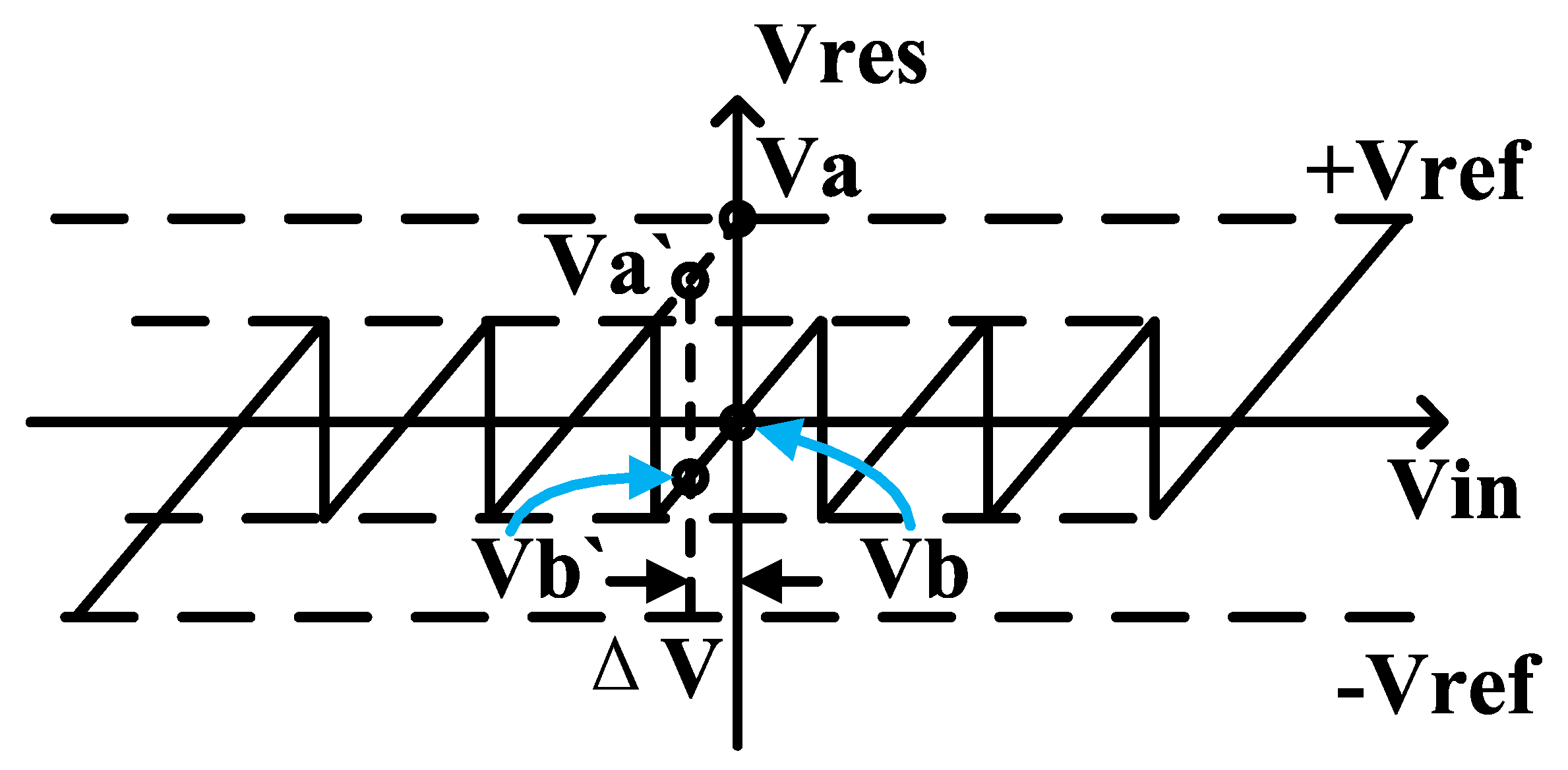
The bit-weight measurement is to obtain the unique jump [18] due to the fabrication mismatches between DAC capacitors in the digital domain. Two measured points (residue voltage of the MDAC) need to be quantized by the backend ADC like Va and Vb shown in Figure 9.
When the conventional bit-weight measurement based on zero-input [18] is applied by the 0.5-bit redundancy MDAC following a 10-bit backend ADC, the quantized residue voltage Va in Figure 9 is expressed as:
D b k _ V a = 0 512 × 1 2 C i C 3 4 6 C j ( 1 + 1 A β ) C f ,
which is around 512. It means that the residue voltage is on the edge of the backend ADC input range as shown in Figure 9. Out-range error would arise with little disturbance. A specific input voltage Δ V is necessary to make the residue voltage located in the backend ADC input range (Va’ and Vb’) as illustrated in Figure 9. By using the capacitor Cd in Figure 8, an equivalent DC input is generated instead of offering a real input voltage. The improved bit-weight measurement is depicted as follows. In the sampling phase, zero input is sampled on the switch capacitors (Cf, Cc and C1~C6), while the capacitor Cd is shorted to ground. As the amplifying phase arrives, the PRBS circuit is controlled by the ctrl_prbs shown in Figure 8 to send a constant signal, making the Cd connected to +Vref. A fixed charge is injected into the signal stored on the switch capacitors, which is equivalent to a DC input Δ V for the quantization of Va’ and Vb’ as shown in Figure 9. And the capacitor under measurement is connected to +Vref and -Vref alternatively for the two quantization. At the same time, two of the remaining DAC capacitors (C1~C6) are connected to +Vref and the rest are connected to -Vref. These operations are performed by externally controlling the digital mux via ctrl_cmp as shown in Figure 8.
The 3rd bit-weight measurement is taken as an instance. The fixed charge is injected by the PRBS circuit via ctrl_prbs. By sending the digital code (110000) of ctrl_cmp, the quantization results of residue voltage (Va’) is given by:
D b k _ V a = 512 × C d ( 1 + 1 A β ) C f 512 × 1 2 C i C 3 4 6 C j ( 1 + 1 A β ) C f ,
with the digital code (111000), the quantization results of residue voltage (Vb’) is given by:
D b k _ V b = 512 × C d ( 1 + 1 A β ) C f 512 × 1 2 C i + C 3 4 6 C j ( 1 + 1 A β ) C f .
Compared with the formula (1), the 1st item in formula (2) and (3) is the residue shift owing to the equivalent DC input described above, which makes the value of D b k _ V a less than 512. Its magnitude is concerned with the ratio of Cd to Cf. An appropriate capacitance of Cd ensures that the output of the MDAC can be covered by the input range of the backend ADC as shown in Figure 9. The 3rd bit-weight is obtained by subtracting formula (3) from formula (2) as formula (4):
H 3 = D b k _ V a D b k _ V b = 512 × 2 C 3 ( 1 + 1 A β ) C f .
The calibration starts from stage 3 to stage 1 and the following stages of the calibrated one operate as the backend ADC while the output reset switch of its preceding stage is reused to set the input to zero. After the foreground calibration, the Cd capacitor can be reused to inject dither signal in the background calibration.

4. Results

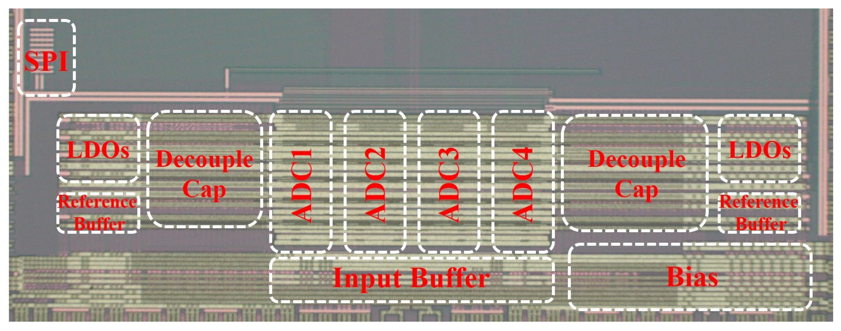
The die micrograph of 3GSps 12-bit pipelined ADC fabricated in 40 nm CMOS is presented in Figure 10. It occupies an active area of 3 mm × 1.3 mm mainly including input buffer, four channels, internal low dropout regulator (LDO) and reference buffer. Besides, the SPI block is placed on the top left corner to receive the control signal and the bias block is on the low right corner to provide the bias current for all blocks. A massive decoupled capacitors are filled in the spaces between different blocks, to absorb transient current for stabilizing the DC voltage.
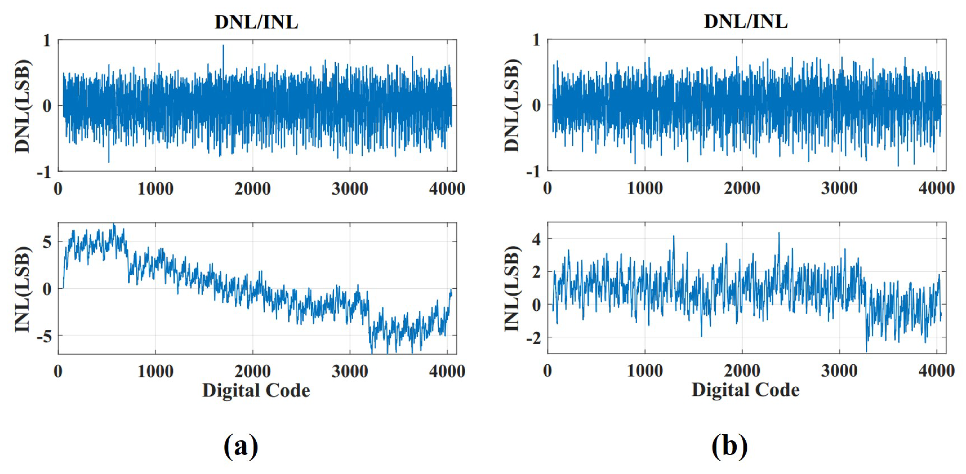
The static performance of the differential nonlinearity (DNL) and integral nonlinearity (INL) is shown in Figure 11. The measured DNL and INL before the zero-input-based calibration are −0.87/+0.92 and −6.95/+6.94 respectively. After the calibration, they are decreased to −0.93/+0.73 LSB and −2.8/+4.3 LSB.
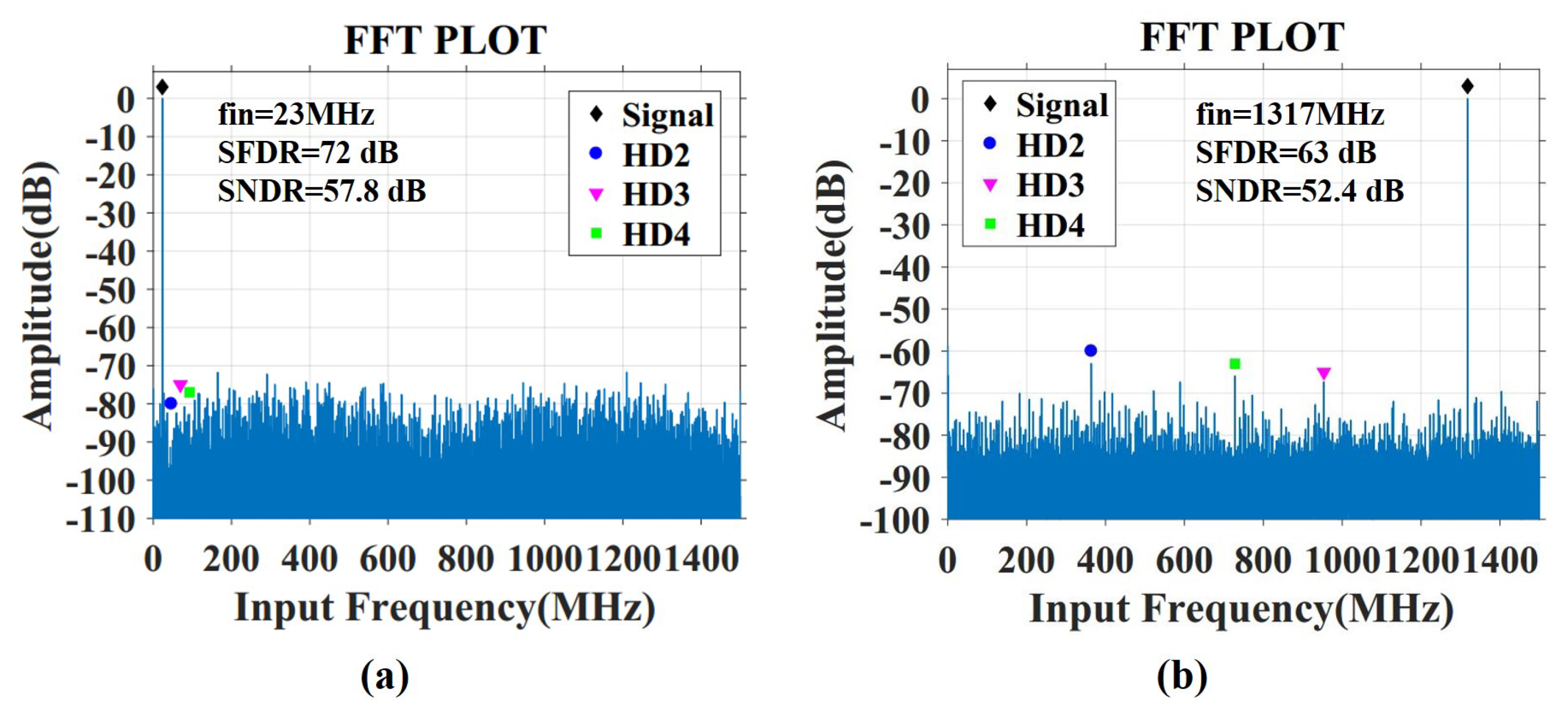
The SFDR and SNDR reach 72 dB and 57.8 dB respectively with a 23 MHz input tone at 3GSps as shown in the fast Fourier transform (FFT) spectrum of Figure 12a. When the input frequency is raised to 1317 MHz, the SFDR and SNDR can maintain 63 dB and 52.4 dB, respectively. As shown in Figure 12b, the 2nd order harmonic (HD2) is the main limitation for SFDR with high input frequency which may be partially contributed by the imbalance of the balun block mounted on PCB.
Figure 13 shows the SFDR and SNDR performance with and without calibration versus the input frequency. The best improvement of about 8 dB is achieved for SFDR by the developed calibration. When the input frequency is above 800 MHz, the improvement of the calibration is attenuated with respect to the input frequency. Meanwhile, the SNDR is slightly improved by the calibration.
The total ADC consumes 450 mW (including the internal LDO and reference buffer) powered at 1.8 V. The figure of merit (FOM) is 0.44 pJ/step according to the formula (5).
F O M = P o w e r 2 ( S N D R 1.76 6.02 ) × f s .

5. Discussion

The results in Section 4 demonstrated the effectiveness of the techniques exploited in this paper. First, the time skew due to channel mismatches is removed with minimal hardware overhead and power consumption. The distortion due to time skew is fully suppressed in both low and high input frequency as shown in Figure 12. However the capacitor-based delay cell in Figure 3 may be unqualified for the higher delay resolution due to thermal and power-supply noise jitter [12]. The delay cell based on current-starved inverter is a good choice when the required delay resolution increases [9]. Second, the FOM improvement shown in Table 1 depends on the early comparison scheme which optimizes the sub-ADC resolving time and the RA settling time and makes a power-efficient CLNC replace the typical NCG. Third, although zero-input-based calibration is well implemented with 1-bit redundancy MDAC for pipelined ADC [18], the out-range error limits the application in 0.5-bit redundancy MDAC. In this paper, the calibration becomes feasible with the dither capacitors and the PRBS circuits, where the INL and DNL is improved as shown in Figure 11 and the dynamic performance can also be ameliorated in a wide band as shown in Figure 13. Moreover, these hardware overhead are not exclusive to the foreground calibration. They can be reused in the background calibration based on correlation.
As the antennas of massive MIMO system grow in quantity for 5G communication, the number of RF chains including ADC and DAC also increases dramatically. The promotion of ADC chip would eventually bring in a large amount of benefits for the whole system. For the base station in 5G communication, it means a higher deployment density and less maintenance expense.

6. Conclusions

This paper presented a 3GSps 12-bit four-channel time-interleaved pipelined ADC for 5G communication. By combining the master clock sampling and delay-adjusting, the time skew due to channel mismatches is removed without a massive capacitor array. And this time skew calibration is not concerned with the ADC quantization principle, which is also adaptive to the interleaving of other ADC architectures [32,33,34]. The early comparison scheme is adopted to optimize the sub-ADC resolving time and the RA settling time. Therefore the typical NCG can be replaced by a developed CLNC owing to the minimized non-overlapping time, which improves the performance and reduces the hardware overhead. Furthermore, the hybrid ADCs based on residue amplification [35,36] become more and more favorable as the technology scales down, where the sampling phase and amplifying phase are still needed. Thus the CLNC is also a potential power-efficient scheme to generate non-overlapping clock instead of typical NCG. The bit-weight of pipelined ADC is measured by a zero-input-based calibration to correct the capacitor mismatch and inter-stage gain error for 0.5-bit redundancy MDAC. Most ADC architectures also have to deal with the capacitor mismatch for highly accurate quantization [33,34,35,36]. This calibration provides an inspiration for estimating the capacitor mismatch through one input voltage and well-defined operations.

Author Contributions

J.L. (Jianwen Li) designed the circuits, analyzed the measurement data, and wrote the manuscript. X.G., J.L. (Jian Luan), D.W. and L.Z. assisted the circuits implementation and simulation. Y.H. assisted the chip package implementation and the PCB designing. N.W. and H.J. performed the chip test. X.Z. and J.W. contributed to the technical discussions and reviewed the manuscript. X.L. gave some valuable guidance and confirmed the final version of manuscript.

Funding

This research was funded by the National Key Research and Development Program of China (Grant No. 2018YFB2202302).

Conflicts of Interest

The authors declare no conflict of interest.

Abbreviations

The following abbreviations are used in this manuscript:
ADCAnalog-to-digital converterThe system that converts an analog signal into a digital signal.
CLNCCustom-designed latch for non-overlapping clockThe circuit that replaces NCG to generate the non-overlapping clock.
CMOSComplementary metal oxide siliconThe basic component of integrated circuits.
DACDigital-to-analog converterThe system that converts a digital signal into an analog signal.
DNLDifferential nonlinearityA term describing the deviation between two analog values corresponding to adjacent input digital values.
FFTFast Fourier transformIt converts a signal from time domain to a representation in the frequency domain.
FIRFinite impulse responseThe impulse response (or response to any finite length input) is of finite duration, because it settles to zero in finite time.
FOMFigure of meritA numerical expression representing the performance or efficiency of a given ADC.
GSpsGiga samples per secondThe unit of sampling rate.
HDHarmonic distortionThe distortion due to the signal whose frequency is an integral multiple of the frequency of the fundamental signal.
INLIntegral nonlinearityA term describing the deviation between the ideal output value and the actual measured output value for a certain input code.
LDOLow dropout regulatorA DC linear voltage regulator that can regulate the output voltage.
MDACMultiplying digital-to-analog converterThe cascaded coarse digitization stage which mainly consist of a sampling switch, a coarse ADC, a digital-to-analog converter (DAC), and a residue amplifier.
MIMOMultiple-input, multiple-outputA method for multiplying the capacity of a radio link using multiple transmission and receiving antennas to exploit multipath propagation.
NCGNon-overlapping clock generatorThe circuit that generates the non-overlapping clock.
PRBSPseudorandom bit sequenceA binary sequence that, while generated with a deterministic algorithm, is difficult to predict and exhibits statistical behavior similar to a truly random sequence.
RAResidue amplifierThe circuit that amplifies the residue signal to full scale.
SFDRSpurious free dynamic rangeStrength ratio of the fundamental signal to the strongest spurious signal in the output, which is measured with the unit of dB scale.
SHASample and hold amplifierThe circuit that is used to sample an analog signal and to store its value for some length of time.
SPISerial peripheral interfaceA synchronous serial communication interface specification used for short-distance communication.
SNDRSignal-to-noise-and-distortion ratioIt stands for the ratio of the signal power to all the unwanted components, which is measured with the unit of dB scale.
SLSampling latchThe sampling clock is retimed by this circuit with master clock.
UCPUnit conversion periodThe time that ADC converts an analog signal to a digital signal once.
VDLVariable delay lineThe circuit that adjusts the delay time of sampling clock.
DCDirect current
IFIntermediate frequency
RFRadio frequency
LSBLeast significant bit
MSBMost significant bit
nMOSn-type metal oxide silicon
pMOSp-type metal oxide silicon
PCBPrinted circuit board

References

  1. Kumar, A.; Ganti, R.K.; Aniruddhan, S. A Same-Channel Full-Duplex Receiver Using Direct RF Sampling. In Proceedings of the 2018 IEEE International Symposium on Circuits and Systems (ISCAS), Florence, Italy, 27–30 May 2018; pp. 1–4. [Google Scholar]
  2. Haberl, M.; Sanftl, B.; Trautmann, M.; Weigel, R.; Koelpin, A. A direct RF-to-baseband quadrature subsampling receiver using a low cost ADC. In Proceedings of the 2017 IEEE Radio and Wireless Symposium (RWS), Phoenix, AZ, USA, 15–18 January 2017; pp. 144–146. [Google Scholar]
  3. Psiaki, M.L.; Powell, S.P.; Hee, J.; Kintner, P.M. Design and practical implementation of multifrequency RF front ends using direct RF sampling. IEEE Trans. Microw. Theory Tech. 2005, 53, 3082–3089. [Google Scholar] [CrossRef]
  4. Thor, J.; Akos, D.M. A direct RF sampling multifrequency GPS receiver. In Proceedings of the 2002 IEEE Position Location and Navigation Symposium, Palms Springs, CA, USA, 15–18 April 2002; pp. 44–51. [Google Scholar]
  5. Doris, K.; Janssen, E.; Nani, C.; Zanikopoulos, A.; Van der Weide, G. A 480 mW 2.6GS/s 10b 65 nm CMOS time-interleaved ADC with 48.5 dB SNDR up to Nyquist. In Proceedings of the 2011 IEEE International Solid-State Circuits Conference, San Francisco, CA, USA, 20–24 February 2011; pp. 180–182. [Google Scholar]
  6. Gupta, S.; Choi, M.; Inerfield, M.; Wang, J. A 1GS/s 11b Time-Interleaved ADC in 0.13 um. In Proceedings of the 2006 IEEE International Solid State Circuits Conference, San Francisco, CA, USA, 6–9 February 2006; pp. 2360–2369. [Google Scholar]
  7. Brandolini, M.; Shin, Y.J.; Raviprakash, K.; Wang, T.; Wu, R.; Geddada, H.M.; Ko, Y.; Ding, Y.; Huang, C.; Shih, W.; et al. A 5 GS/s 150 mW 10 b SHA-Less Pipelined/SAR Hybrid ADC for Direct-Sampling Systems in 28 nm CMOS. IEEE J. Solid-State Circuit 2015, 50, 2922–2934. [Google Scholar] [CrossRef]
  8. Janssen, E.; Doris, K.; Zanikopoulos, A.; Murroni, A.; Weide, G.; Lin, Y.; Alvado, L.; Darthenay, F.; Fregeais, Y. An 11b 3.6 GS/s time-interleaved SAR ADC in 65 nm CMOS. In Proceedings of the 2013 IEEE International Solid-State Circuits Conference, San Francisco, CA, USA, 17–21 February 2013; pp. 464–465. [Google Scholar]
  9. Wei, H.; Zhang, P.; Sahoo, B.D.; Razavi, B. An 8 Bit 4 GS/s 120 mW CMOS ADC. IEEE J. Solid-State Circuit 2014, 49, 1751–1761. [Google Scholar] [CrossRef]
  10. Razavi, B. Design Considerations for Interleaved ADCs. IEEE J. Solid-State Circuit 2013, 48, 1806–1817. [Google Scholar] [CrossRef] [Green Version]
  11. Jamal, S.M.; Fu, D.; Hurst, P.J.; Lewis, S.H. A 10b 120 MSample/s time-interleaved analog-to-digital converter with digital background calibration. In Proceedings of the 2002 IEEE International Solid-State Circuits Conference, San Francisco, CA, USA, 7 February 2002; pp. 172–457. [Google Scholar]
  12. El-Chammas, M.; Murmann, B. A 12-GS/s 81-mW 5-bit Time-Interleaved Flash ADC With Background Timing Skew Calibration. IEEE J. Solid-State Circuit 2011, 46, 838–847. [Google Scholar] [CrossRef]
  13. Mcneil, J.A.; David, C.; Coin, M.; Croughwell, R. “Split ADC” Calibration for All-Digital Correction of Time-Interleaved ADC Errors. IEEE Trans. Circuits Syst. II Express Briefs 2009, 56, 344–348. [Google Scholar] [CrossRef]
  14. Haftbaradaran, A.; Martin, K.W. A Sample-Time Error Compensation Technique for Time-Interleaved ADC Systems. In Proceedings of the 2007 IEEE Custom Integrated Circuits Conference, San Jose, CA, USA, 16–19 September 2007; pp. 341–344. [Google Scholar]
  15. Huang, S.; Levy, B.C. Adaptive blind calibration of timing offset and gain mismatch for two-channel time-interleaved ADCs. IEEE Trans. Circuits Syst. I Regul. Pap. 2006, 53, 1278–1288. [Google Scholar] [CrossRef]
  16. Stepanovic, D.; Nikolic, B. A 2.8 GS/s 44.6 mW Time-Interleaved ADC Achieving 50.9 dB SNDR and 3 dB Effective Resolution Bandwidth of 1.5 GHz in 65 nm CMOS. IEEE J. Solid-State Circuit 2013, 48, 971–982. [Google Scholar] [CrossRef]
  17. Khalil, R.; Louerat, M.M.; Petigny, R.; Gicquel, H. Background offset and gain calibration for time-interleaved ADC using digital sinusoidal calibration signal. In Proceedings of the 2012 International Conference on Synthesis, Modeling, Analysis and Simulation Methods and Applications to Circuit Design (SMACD), Seville, Spain, 19–21 September 2012; pp. 273–276. [Google Scholar]
  18. Zheng, X.; Wang, Z.; Li, F.; Zhao, F.; Yue, S.; Zhang, C.; Wang, Z. A 14-bit 250 MS/s IF Sampling Pipelined ADC in 180 nm CMOS Process. IEEE Trans. Circuits Syst. I Regul. Pap. 2016, 63, 1381–1392. [Google Scholar] [CrossRef] [Green Version]
  19. Ali, A.M.A.; Dinc, H.; Bhoraskar, P.; Dillon, C.; Puckett, S.; Gray, B.; Speir, C.; Lanford, J.; Brunsilius, J.; Derounian, P.R.; et al. A 14 Bit 1 GS/s RF Sampling Pipelined ADC With Background Calibration. IEEE J. Solid-State Circuit 2014, 49, 2857–2867. [Google Scholar] [CrossRef]
  20. Chiu, Y.; Tsang, C.W.; Nikolic, B.; Gray, P.R. Least mean square adaptive digital background calibration of pipelined analog-to-digital converters. IEEE Trans. Circuits Syst. I-Regul. Pap. 2004, 51, 38–46. [Google Scholar] [CrossRef]
  21. Moon, U.-K.; Song, B.-S. Background digital calibration techniques for pipelined ADCs. IEEE Trans. Circuits Syst. II 1997, 44, 102–109. [Google Scholar] [CrossRef] [Green Version]
  22. Grace, C.R.; Hurst, P.J.; Lewis, S.H. A 12-bit 80-MSample/s pipelined ADC with bootstrapped digital calibration. IEEE J. Solid-State Circuit 2005, 40, 1038–1046. [Google Scholar] [CrossRef] [Green Version]
  23. Ali, A.M.A.; Nagaraj, K. Background calibration of operational amplifier gain error in pipelined A/D converters. IEEE Trans. Circuits Syst. II 2003, 50, 631–634. [Google Scholar]
  24. Jalali-Farahani, B.; Meruva, A. A 14-b 32 MS/s pipelined ADC with fast convergence comprehensive background calibration. Analog Integr. Circuits Process. 2009, 61, 65–74. [Google Scholar] [CrossRef]
  25. Chiang, S.W.; Sun, H.; Razavi, B. A 10-Bit 800-MHz 19-mW CMOS ADC. In Proceedings of the 2013 Symposium on VLSI Circuits, Kyoto, Japan, 12–14 June 2013; pp. C100–C101. [Google Scholar]
  26. Min, B.M.; Kim, P.; Bowman, F.W.; Boisvert, D.M.; Aude, A.J. A 69-mW 10-bit 80-MSample/s Pipelined CMOS ADC. IEEE J. Solid-State Circuit 2003, 38, 2031–2039. [Google Scholar]
  27. Lien, Y.C. A 14.6 mW 12b 800MS/s 4× time-interleaved pipelined SAR ADC achieving 60.8 dB SNDR with Nyquist input and sampling timing skew of 60fsrms without calibration. In Proceedings of the 2016 IEEE Symposium on VLSI Circuits (VLSI-Circuits), Honolulu, HI, USA, 15–17 June 2016; pp. 1–2. [Google Scholar]
  28. Pu, J.; Shen, X.; Huang, X.; Fu, D.; Zhang, R. A 14-bit 500 MS/s low power time-interleaved analog-to-digital converter in 0.18-uM CMOS technology with background calibration. In Proceedings of the 2014 12th IEEE International Conference on Solid-State and Integrated Circuit Technology (ICSICT), Guilin, China, 28–31 October 2014; pp. 1–3. [Google Scholar]
  29. Cho, T.B.; Gray, P.R. A 10 b, 20 Msample/s, 35 mW pipeline A/D converter. IEEE J. Solid-State Circuit 1995, 30, 166–172. [Google Scholar] [CrossRef]
  30. Lewis, S.H.; Fetterman, H.S.; Gross, G.F.; Ramachandran, R.; Viswanathan, T.R. A 10-b 20-Msample/s analog-to-digital converter. IEEE J. Solid-State Circuit 1992, 27, 351–358. [Google Scholar] [CrossRef] [Green Version]
  31. Hsu, C.; Huang, F.; Shih, C.; Huang, C.; Lin, Y.; Lee, C.; Razavi, B. An 11b 800MS/s Time-Interleaved ADC with Digital Background Calibration. In Proceedings of the 2007 IEEE International Solid-State Circuits Conference, San Francisco, CA, USA, 11–15 February 2007; pp. 464–615. [Google Scholar]
  32. Zhong, Y.; Li, S.; Tang, X.; Shen, L.; Zhao, W.; Wu, S.; Sun, N. A Second-Order Purely VCO-Based CT ΔΣ ADC Using a Modified DPLL Structure in 40-nm CMOS. IEEE J. Solid-State Circuit 2019. [Google Scholar] [CrossRef]
  33. Shen, Y.; Tang, X.; Shen, L.; Zhao, W.; Xin, X.; Liu, S.; Zhu, Z.; Sathe, V.S.; Sun, N. A 10-bit 120-MS/s SAR ADC With Reference Ripple Cancellation Technique. IEEE J. Solid-State Circuit 2019. [Google Scholar] [CrossRef]
  34. Cho, S.; Lee, C.; Lee, S.; Ryu, S.R. A Two-Channel Asynchronous SAR ADC With Metastable-Then-Set Algorithm. IEEE Trans. Very Large Scale Integr. (VLSI) Syst. 2012, 20, 765–769. [Google Scholar] [CrossRef]
  35. Moon, K.; Jo, D.; Kim, W.; Choi, M.; Ko, H.; Ryu, S. A 9.1-ENOB 6-mW 10-Bit 500-MS/s Pipelined-SAR ADC With Current-Mode Residue Processing in 28-nm CMOS. IEEE J. Solid-State Circuit 2019, 54, 2532–2542. [Google Scholar] [CrossRef]
  36. Seo, M.; Kim, Y.; Chung, J.; Ryu, S. A 40nm CMOS 12b 200 MS/s Single-amplifier Dual-residue Pipelined-SAR ADC. In Proceedings of the 2019 Symposium on VLSI Circuits, Kyoto, Japan, 9–14 June 2019; pp. C72–C73. [Google Scholar]
Figure 1. Proposed four-channel time-interleaved pipelined analog-to-digital converter (ADC).
Electronics 08 01551 g001
Figure 2. Illustration of the calibration for multiplying digital-to-analog converter (MDAC) stage.
Electronics 08 01551 g002
Figure 3. (a) Ideal timing diagram for the master clock sampling; (b) Block diagram of the retiming scheme combined with delay-adjusting.
Electronics 08 01551 g003
Figure 4. (a) The sampled waveform with time skew; Block diagram for the detection of the timing mismatch (b) Δ T2, (c) Δ T1 and (d) Δ T3.
Electronics 08 01551 g004
Figure 5. (a) The comparator for the sub-ADC; Timing diagram for the comparators in (b) the 1st stage (c) and the rest stages.
Electronics 08 01551 g005
Figure 6. (a) Illustration of the common-mode mismatch between input and reference; (b) The feedback circuit for cancelling the common-mode mismatch.
Electronics 08 01551 g006
Figure 7. (a) Circuit implementation of the custom-designed latch for non-overlapping clock (CLNC); (b) Timing diagram for the CLNC.
Electronics 08 01551 g007
Figure 8. The proposed 0.5-bit redundancy MDAC architecture.
Electronics 08 01551 g008
Figure 9. The bit-weight measurement illustrated with the residue transfer curve.
Electronics 08 01551 g009
Figure 10. The die micrograph.
Electronics 08 01551 g010
Figure 11. The static performance of DNL/INL(a) with and (b) without the zero-input-based calibration.
Electronics 08 01551 g011
Figure 12. The measured fast Fourier transform (FFT) spectrum at 3GSps for the input frequency (a) 23 MHz and (b) 1317 MHz.
Electronics 08 01551 g012
Figure 13. Measured signal-to-noise distortion ratio (SNDR) and spurious free dynamic range (SFDR) performance versus input frequency at 3GSps.
Electronics 08 01551 g013
Table 1. Summarizes the performance of this work and comparison with state-of-art ADCs.
Reference[8][5][6][31]This Work
ProcessCMOS 65 nmCMOS 65 nmCMOS 0.13 μ mCMOS 90 nmCMOS 40 nm
Sampling rate(MSps)3600260010008003000
Resolution(bits)1110111112
Supply(V)1.2/2.51.2/1.3/1.61.2/2.51.3/1.51.8
SNDR@Nyquist(dB)4248.5525452.3
SFDR@Nyquist(dB)5053.853.16061.5
Power(W)0.7950.480.250.350.45
FOM@Nyquist(pJ/step)2.150.850.51.10.44