1. Introduction
From low speed applications such as industrial monitoring, bio-medical and sensor node [
1,
2,
3] to high speed applications such as high speed links and next generation communication systems [
4,
5], Successive Approximate Register (SAR) ADC is the most widely adopted ADC architecture owing to its low power operation from a simple operating principle. Moreover, an asynchronous architecture is also widely used to mitigate the requirements of the comparison time of the comparator in SAR ADC.
In the asynchronous SAR ADC, the time budget of the sampling clock is composed of an input sample time, comparator comparison time, capacitor DAC settling time, digital logic propagation delay, and the number of repetitions proportional to the resolution, as shown in
Figure 1. While many studies have been conducted to reduce each timing budget to enhance the ADC performance, the loop delay that replaces the DAC settling time has been subjected to few methodological studies. Therefore, this paper focuses on digitally controlled delay generation methods with linear delay characteristics when the asynchronous SAR ADC has a sampling frequency of several MS/s. The linear delay characteristics can be applied to design the loop delay circuit of SAR ADC with reconfigurable sampling frequency or tapered bit periods [
6,
7]. For the SAR ADC of this paper, we designed an ADC with reconfigurable sampling frequency to obtain an adjustable frame rate in a touch screen panel (TSP) readout IC.
There are several ways to implement a digitally controlled variable delay cell. The popular method is a delay cell with shunt capacitors [
8]. Assuming that the delay cell is a first-order RC circuit, this delay cell adjusts the capacitance depending on the digital input patterns. Similarly, a method adjusting the resistance in the first-order RC circuit was introduced in reference [
9]. An MOS transistor array was used as a variable resistor. Another method used to generate a digitally controlled delay cell is a current starved architecture [
10]. The delay cell adopts a tail current source, thus adjusting delay by digitally controlled current level. Using digital logic propagation delay is another way to implement a digitally controlled delay cell [
11]. This method adjusts the delay by varying the number of logic gates.
When the delay cell is applied to the asynchronous SAR ADC, with sampling frequency of few MS/s and medium resolution, the delay cell should have a delay value of several tens of nanoseconds. Thus, the delay generation methods using the logic propagation delay and variable capacitance are inadequate due to power consumption in proportion to delay. In addition, the current staved structure requires an analog bias voltage, which leads to static current consumption by an additional bias generation circuit. In the case of using a MOS transistor as a variable resistor, the coding problem occurs due to the unpredictable circuit characteristic when the delay is generated by the equivalent resistance value.
Among the methods used to generate delay, the proposed delay cell adopts a resistive controlled delay cell to achieve high linearity with low power consumption. Thus, the proposed delay cell replaces the MOS transistor array to passive resistors to avoid the nonlinear delay characteristic and code dependent parasitic capacitance of the active device. The structure of the proposed delay cell is described in
Section 2, along with the analysis of the linearity of the delay. The detailed circuit implementation of the proposed delay cell is represented in
Section 3 with a delay calibration method. Finally, the simulation and measurement results are shown in
Section 4, and we conclude the paper in
Section 5.
2. Linearity of Delay Cell
Figure 2 shows a simple delay cell structure with a RC low-pass filter. When the input changes from high to low, the output voltage
can be expressed as a first order response given as
where
is supply voltage of delay cell. Then, we can solve the (1) for
, yielding
Assuming that a logical signal is delivered to the next digital logic when the voltage settling is about 50 percent, the final value of
can be approximated to be
. Then, the logarithm term in (2) can be replaced by a constant coefficient
. Thus, the calculated delay time for the time constant can be expressed as
where
is the turn on resistance of the P-type MOS transistor. From (3), the resistance
, capacitance
and equivalent resistance of the MOS transistor
are the factors that can adjust the delay time. However, adjusting
is difficult, because the power consumption of delay cell is proportional to
. In addition, using turn on resistance
of the transistor is also not suitable due to the poor linearity of delay from the nonlinear characteristic of active devices. Therefore, adjusting
is the most reasonable approach in terms of power consumption and delay linearity. Then, we obtain a linear delay step according to the derivation of
which is given as
It is important that the effect on , which causes the nonlinearity, is eliminated in the resistive controlled delay cell.
The proposed digitally controlled delay cell is shown in
Figure 3. The resistance is controlled by a switch with a small resistance value.
is the parasitic capacitance of the switch. As the switch is made of a pass transistor, the parasitic capacitance changes depending on whether the switches are on or off.
is sum of the parasitic capacitances for all pass transistors.
From (3) the delay time is a calculated by the product of time constant of the circuit and constant coefficient . In other words, we can obtain the delay time by calculating the time constant of delay cell. To derive the time constant of entire RC network of proposed delay circuit, the Elmore delay model is employed.
Figure 4 represents the RC network model of proposed delay cell.
is the turn on resistance of a switch made of pass transistor.
and
are parasitic capacitances of turn on and off switch, respectively. Among the switches, only one switch is turned on as the digital control input, so the internal RC network connected in parallel with the
must be converted to a network, to which the Elmore delay model is applicable.
To simplify the internal RC network,
Figure 5 describes a lumped PI-T transform method [
12]. After calculating the time constant of PI and T model using Elmore delay model, two relations of the lumped PI-T transform are given as
Using the lumped PI-T transform, the internal RC network can be simplified in the form of PI, and the parameters of the simplified PI model
and
are calculated as
where
is the number of
in the internal RC network.
Figure 6 shows the RC network model of proposed delay cell using (6).
represents the total number of switches. Assuming that
is much smaller than
, the resistance of parallel resistors can be approximated as
Then, the normalized time constant equation of the proposed delay cell can be obtained as
where
Finally, the delay step can be obtained by the difference between the previous and current step of the normalized time constant from (4) and is derived as
It is important to note that the nonlinearity of proposed delay cell is determined by the term multiplied by the value of
. If
is large enough, Equation (9) can be approximated as
The term including is very small and hence negligible. If is not in (10), then the delay linearity of the proposed structure has an error of approximately ±12.5 percent at maximum. In order to attain more linearity, the passive capacitor is added at the cost of the increased power consumption.
3. Circuit Implementation
The implementation of loop delay circuit for asynchronous SAR ADC is presented in
Figure 7. This circuit senses the comparison completion of the comparator and makes the comparator reset and operation clock repeatedly. The detailed circuit operation is as follows. When the START generated by inverting the sampling clock goes high, the loop is activated and the first comparison is made as the comparator clock COMP_CLK goes high. After the comparison of the comparator, the COMP_DONE indicating the end of the comparison becomes high and quickly resets COMP_CLK through the comparator reset path. As the comparator is reset, COMP_DONE is also reset. Then, the low state of COMP_DONE is propagated through DAC settling path, and COMP_CLK becomes high again after a propagation delay of delay cell. This SAR operation loop is repeated until the STOP goes high after all conversion cycles have ended.
One feature of the loop delay circuit is that it is divided into the DAC settling path and the comparator reset path depending on the logical state of COMP_DONE. This two path operation has the advantage of using both fast and slow signal passing. However, the internal node of the delay cell can be in undesired states when the low state is applied to the delay cell input, because the input of the delay cell may change before the internal logical states by earlier high state input are entirely propagated. To prevent these uncertain states in the proposed delay cell, it includes reset switches as shown in
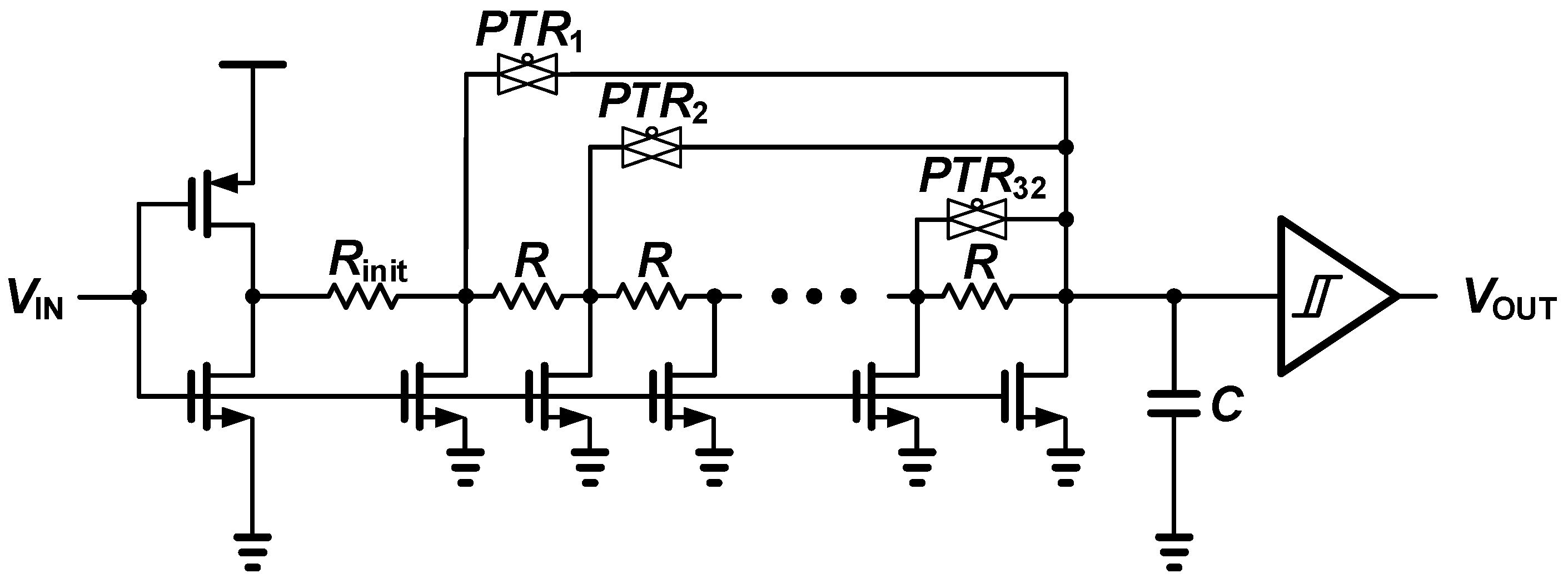
Figure 8. The reset switches quickly reset the internal nodes of the delay cell when the comparator reset path is activated. The delay cell is controlled by 5-bit digital input, hence 32 resistors and switches consist of a proposed delay cell.
, representing the first passive resistance, is replaced by a lager resistance, instead of
, to increase the minimum delay. In addition, a Schmitt trigger is employed at the output stage to prevent any glitch caused by the supply fluctuations [
13].
The main drawback of using a passive resistor is that the resistance in the silicon process varies significantly with the process corner or temperature. Particularly, the delay variation is mostly dominated by process variation rather than temperature variation. To resolve this process variation, a foreground calibration is performed for the loop delay circuit. The delay is calibrated so that the STOP indicating the end of the conversion is aligned with the rising edge of next track and hold clock, as shown in
Figure 7. Moreover, an additional DAC settling cycle is added to cover the temperature variation, hence securing a 1 cycle margin.
4. Simulation and Measurement Results
Figure 9a shows the calculated delay times from (8) with simulated delays from SPICE simulation according to the input digital codes. In the proposed delay cell,
and
are 15.1
and 1.9
, respectively, at the nominal corner.
and
are 2.77
and 3.45
, respectively, and are extracted by the SPICE simulation. Because foreground calibration is performed to correct the delay mismatch from process variation, the delays in all corner conditions meet the 15
after calibration. The gray lines show the delays as temperature variations at a nominal corner. Compared to the corner variation, the delay variation from the temperature variation is very small, which is covered by the 1 cycle margin. The calculated delay values reflected the different
values of (3) as the temperature and corner.
and
also reflected the temperature and corner variation.
Figure 9b shows the step delays from SPICE simulation of the proposed delay cell. The proposed delay cell achieves an error of about 5 percent, owing to the additional 155
of Metal-Oxide-Metal (MOM) capacitor
to improve linearity.
Figure 10 shows simulation results of best and worst delay errors by component mismatch. From 200 samples of a Monte Carlo simulation, the best and worst delay error are 2.8 percent and 4.4 percent, respectively, with a mean of 3.6 percent and a standard derivation of 0.2 percent. Thus, the effect of mismatch does not significantly affect the delay linearity.
Table 1 shows the comparison of delay cell structures with respect to current consumption and delay error. In the case of the current staved delay cell, we followed the design procedure of reference [
10] with 30
of load capacitor. For fair comparison, the current consumption is measured with clock frequency of 20 MHz, and the each digital codes that adjusts the delay is set to 15ns. In terms of current consumption, the current starved delay cell has low current consumption. However, it has a 45 percent delay error, which is inadequate for tapered bit periods and reconfigurable sampling frequency. Contrarily, the shunt capacitor based delay cell has high linearity but consumes too much current. In case of the passive resistor based delay cell without
, the delay error is 8 percent with same current level of the current starved delay cell. To reduce delay error, the passive capacitor
is added in our application with additional 10 percent of current consumption. In the total power consumption of ADC, the passive resistor based delay cell consumes 28.4 μW.
Figure 11 shows the signal to noise and distortion ratio (SNDR) performance of prototype SAR ADC according to the delay codes. As the delay code increases, LSB conversions are not performed due to increased DAC settling delay at a given time, hence degrading SNDR performance. In order to use the proposed delay cell for the ADC with reconfigurable sampling frequency, two frequencies and their corresponding delay codes are required to obtain the relation equation. For example, measuring the sampling frequency of prototype SAR ADC at 2 MHz and 3 MHz from two delay calibrations, the corresponding delay codes from calibration are 0 and 11, respectively. Then, in the case of 2.5 MHz, the calculated delay code is 5.5 from the relation equation made with a two point calibration, and thus, delay code of 5 is applied, which is well matched to the measurement at a 2.5 MHz sampling frequency. The delay codes where the bits are skipped also show that the delay cell is sufficiently linear to be utilized for the ADC with a varied sampling frequency.
The prototype SAR ADC is fabricated in the 40 nm CMOS process.
Figure 12 shows the die photograph of prototype SAR ADC, which occupies a core area measuring 670
80
. The delay cell occupies 35
17
, which is about 1 percent of total area. The prototype SAR ADC operates under 1.1 V supply voltage, consuming 67 μW at the 3 MHz sampling frequency.
Figure 13 shows the differential nonlinearity (DNL) and integral nonlinearity (INL). The peak DNL are 2.9/-1 LSB, and the peak INL are 5.8/−10.5 LSB.
Figure 14 shows an output spectrum from the prototype SAR ADC for near 100 kHz and 1.5 MHz. With a near 100 kHz input frequency, a measured spurious free dynamic range (SFDR) and SNDR are 68 dB and 59.4 dB, respectively. With a near 1.5 MHz input frequency, the prototype ADC achieves an SFDR of 65.2 dB and SNDR of 57.4 dB, yielding a FoM of 35.4 fJ/conversion-step. The overall performance of the prototype ADC is summarized in
Table 2 and compared to references [
14,
15,
16,
17].


