A Simplified Methodology to Evaluate Circuit Complexity: Doherty Power Amplifier as a Case Study


Abstract
:1. Introduction
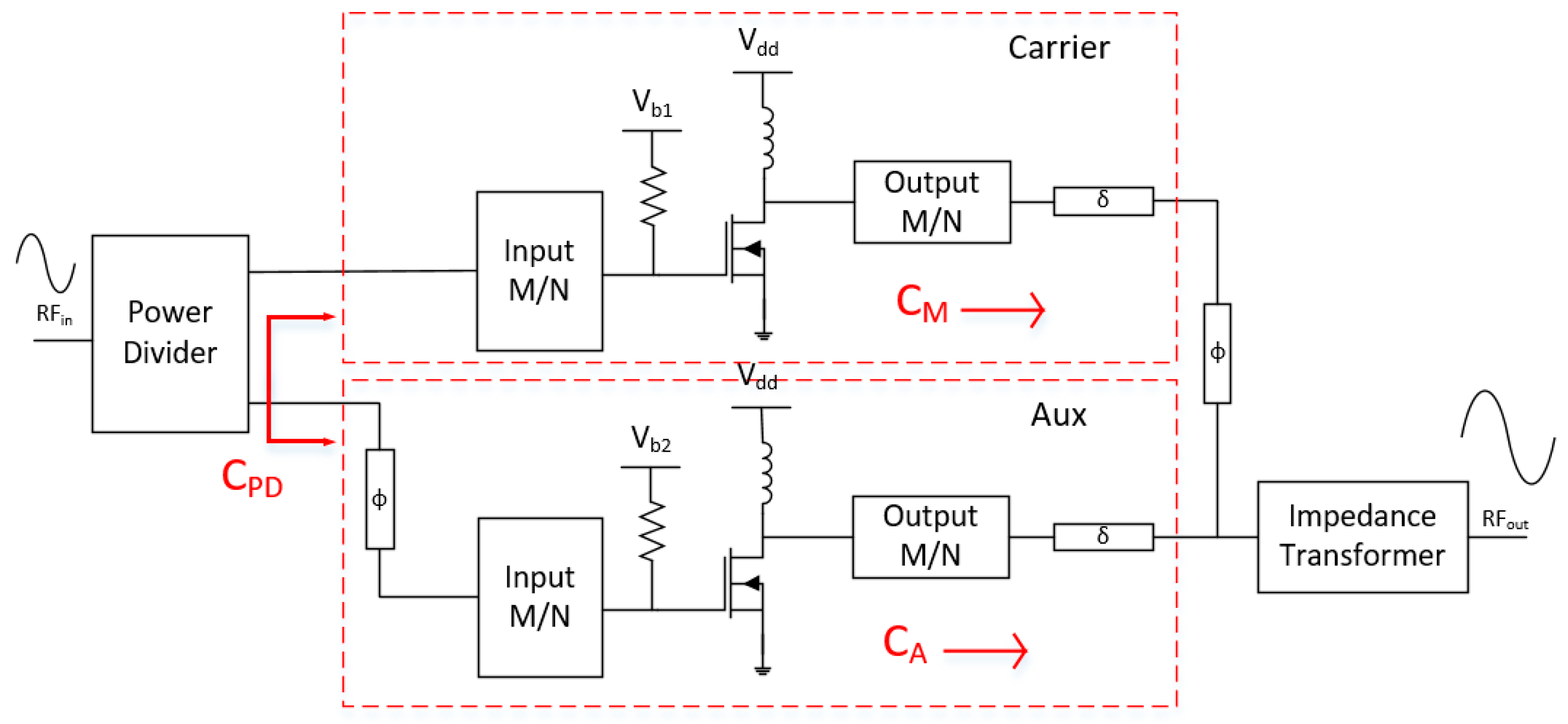
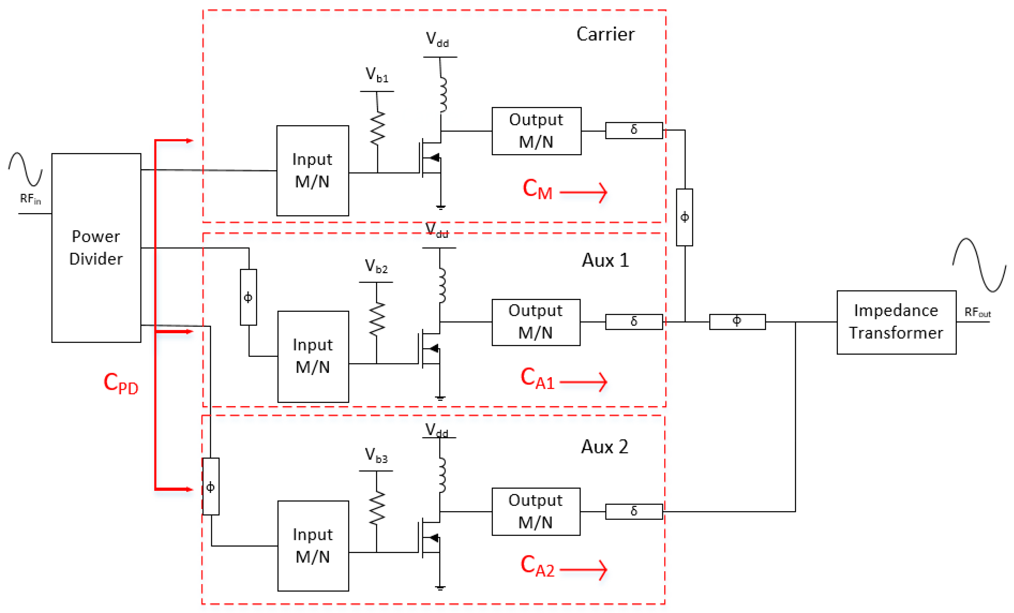
2. Complexity Analysis Using DPA
- is the complexity number for the power divider
- is the complexity number for the power amplifier
- is the complexity number for the matching network.
3. Proposed Complexity Factor For DPA
- = 2 for T-line model
- = 3 for discrete model
4. Experiments and Discussions
5. Conclusions
Author Contributions
Funding
Conflicts of Interest
References
- Doherty, W.H. A New High Efficiency Power Amplifier for Modulated Waves. Proc. Inst. Radio Eng. 1936, 24, 1163–1182. [Google Scholar]
- Enjun, X.; Yuan, J.S.; Hong, Y. CMOS RF and DC reliability subject to hot carrier stress and oxide soft breakdown. IEEE Trans. Device Mater. Reliab. 2004, 4, 92–98. [Google Scholar]
- Venkatasubramanian, R.; Chang, D.; Ozev, S. Analysis and Mitigation of Electromigration in RF Circuits: An LNA Case Study. In Proceedings of the Sixteenth IEEE European Test Symposium, Trondheim, Norway, 23–27 May 2011; p. 215. [Google Scholar]
- Fang, X.; Cheng, K.K.M. Broadband, wide efficiency range, Doherty Amplifier design using frequency-varying Complex Combining Load. In Proceedings of the IEEE MTT-S International Microwave Symposium 2015, Phoenix, AZ, USA, 17–22 May 2015; pp. 1–4. [Google Scholar]
- Kim, C.H.; Jee, S.; Jo, G.D.; Lee, K.; Kim, B. A 2.14-GHz GaN MMIC Doherty Power Amplifier for Small-Cell Base Stations. IEEE Microw. Wirel. Compon. Lett. 2014, 24, 263–265. [Google Scholar] [CrossRef]
- Camarchia, V.; Pirola, M.; Quaglia, R.; Jee, S.; Cho, Y.; Kim, B. The Doherty Power Amplifier: Review of Recent Solutions and Trends. IEEE Trans. Microw. Theory Tech. 2015, 63, 559–571. [Google Scholar] [CrossRef] [Green Version]
- Chen, K.; Lee, J.; Chappell, W.J.; Peroulis, D. Co-Design of Highly Efficient Power Amplifier and High-Q Output Bandpass Filter. IEEE Trans. Microw. Theory Tech. 2013, 61, 3940–3950. [Google Scholar] [CrossRef]
- Fang, X.H.; Liu, H.Y.; Cheng, K.K.M.; Boumaiza, S. Two-Way Doherty Power Amplifier Efficiency Enhancement by Incorporating Transistors’ Nonlinear Phase Distortion. IEEE Microw. Wirel. Compon. Lett. 2018, 28, 168–170. [Google Scholar] [CrossRef]
- Srirattana, N.; Raghavan, A.; Heo, D.; Allen, P.E.; Laskar, J. Analysis and design of a high-efficiency multistage Doherty power amplifier for wireless communications. IEEE Trans. Microw. Theory Tech. 2005, 53, 852–860. [Google Scholar] [CrossRef]
- Fang, X.H.; Cheng, K.K.M. Improving Power Utilization Factor of Broadband Doherty Amplifier by Using Bandpass Auxiliary Transformer. IEEE Trans. Microw. Theory Tech. 2015, 63, 2811–2820. [Google Scholar] [CrossRef]
- Chen, S.; Xue, Q. Optimized Load Modulation Network for Doherty Power Amplifier Performance Enhancement. IEEE Trans. Microw. Theory Tech. 2012, 60, 3474–3481. [Google Scholar] [CrossRef]
- Lee, J.; Lee, D.H.; Hong, S. A Doherty Power Amplifier with a GaN MMIC for Femtocell Base Stations. IEEE Microw. Wirel. Compon. Lett. 2014, 24, 194–196. [Google Scholar] [CrossRef]
- Lee, Y.S.; Lee, M.W.; Jeong, Y.H. Highly Efficient Doherty Amplifier Based on Class-E Topology for WCDMA Applications. IEEE Microw. Wirel. Compon. Lett. 2008, 18, 608–610. [Google Scholar] [CrossRef]
- Lee, M.W.; Kam, S.H.; Lee, Y.S.; Jeong, Y.H. Design of Highly Efficient Three-Stage Inverted Doherty Power Amplifier. IEEE Microw. Wirel. Compon. Lett. 2011, 21, 383–385. [Google Scholar] [CrossRef]
- Kang, J.; Yu, D.; Min, K.; Kim, B. A Ultra-High PAE Doherty Amplifier Basedon 0.13-um CMOS Process. IEEE Microw. Wirel. Compon. Lett. 2006, 16, 505–507. [Google Scholar] [CrossRef]
- Lee, H.; Lim, W.; Bae, J.; Lee, W.; Kang, H.; Hwang, K.C.; Lee, K.Y.; Park, C.S.; Yang, Y. Highly Efficient Fully Integrated GaN-HEMT Doherty Power Amplifier Based on Compact Load Network. IEEE Trans. Microw. Theory Tech. 2017, 65, 5203–5211. [Google Scholar] [CrossRef]
- Jee, S.; Yunsik, P.; Cho, Y.; Lee, J.; Seokhyeon, K.; Bumman, K. A highly linear dual-band Doherty power amplifier for femto-cell base stations. In Proceedings of the IEEE MTT-S International Microwave Symposium 2015, Phoenix, AZ, USA, 17–22 May 2015; pp. 1–4. [Google Scholar]
- Rubio, J.M.; Fang, J.; Camarchia, V.; Quaglia, R.; Pirola, M.; Ghione, G. 3–3.6-GHz Wideband GaN Doherty Power Amplifier Exploiting Output Compensation Stages. IEEE Trans. Microw. Theory Tech. 2012, 60, 2543–2548. [Google Scholar] [CrossRef]
- Probst, S.; Martinelli, T.; Seewald, S.; Geck, B.; Manteuffel, D. Design of a linearized and efficient doherty amplifier for C-band applications. In Proceedings of the 2017 12th European Microwave Integrated Circuits Conference (EuMIC), Nuremberg, Germany, 12 October 2017; pp. 121–124. [Google Scholar]
- Hamed, A.; Aref, A.; Saeed, M.; Negra, R. Doherty power amplifier in 28 nm CMOS for 5G applications. In Proceedings of the 11th German Microwave Conference (GeMiC), Freiburg, Germany, 12–14 March 2018; pp. 191–194. [Google Scholar]
- Gustafsson, D.; Cahuana, J.C.; Kuylenstierna, D.; Angelov, I.; Rorsman, N.; Fager, C. A Wideband and Compact GaN MMIC Doherty Amplifier for Microwave Link Applications. IEEE Trans. Microw. Theory Tech. 2013, 61, 922–930. [Google Scholar] [CrossRef]
- Lin, Y.A.; Ji, J.R.; Chien, T.H.; Chang, H.Y.; Wang, Y.C. A Ka-band 25-dBm output power high efficiency monolithic Doherty power amplifier in 0.15-um GaAs E-mode pHEMT process. In Proceedings of the IEEE Asia Pacific Microwave Conference (APMC), Yokohama, Japan, 13–16 November 2017; pp. 984–987. [Google Scholar]
- Nguyen, D.P.; Curtis, J.; Pham, A.V. A Doherty Amplifier with Modified Load Modulation Scheme Based on Load-Pull Data. IEEE Trans. Microw. Theory Tech. 2018, 66, 227–236. [Google Scholar] [CrossRef]
- Agah, A.; Dabag, H.T.; Hanafi, B.; Asbeck, P.M.; Buckwalter, J.F.; Larson, L.E. Active Millimeter-Wave Phase-Shift Doherty Power Amplifier in 45-nm SOI CMOS. IEEE J. Solid-State Circuits 2013, 48, 2338–2350. [Google Scholar] [CrossRef]
- Liang, C.; Roblin, P.; Hahn, Y.; Xiao, Y. Automatic Algorithm for the Direct Design of Asymmetric Doherty Power Amplifiers. In Proceedings of the IEEE Topical Conference on RF Power Amplifiers for Radio and Wireless Applications, Orlando, FL, USA, 20–23 January 2019. [Google Scholar]


| DPA Blocks | Complexity Variables | Complexity Number | ||
|---|---|---|---|---|
| Discrete Passives | T-Line Passives | Hybrid Passives | ||
| Power Divider | 9 | 9 | 9 | |
| Main Branch | 4 | 4 | 4 | |
| 2 | 4 | 3 | ||
| 2 | 4 | 3 | ||
| 6 | 4 | 4 | ||
| 96 | 256 | 144 | ||
| Auxiliary Branch | 4 | 4 | 4 | |
| 2 | 4 | 3 | ||
| 2 | 4 | 3 | ||
| 6 | 4 | 4 | ||
| 96 | 256 | 144 | ||
| CF | 1728 | 4608 | 2592 | |
| Types of Passive Components | Complexity Factor |
|---|---|
| Discrete | 1728 |
| T-Line | 4608 |
| Hybrid | 2592 |
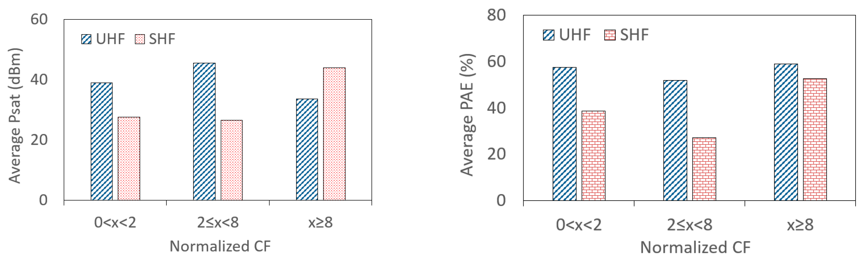
| Freq (GHz) | Psat (dBm) | PAE (%) | G (dB) | NCF | PA FoM | Ref. |
|---|---|---|---|---|---|---|
| 1.55 | 42 | 58.4 | 14 | 8.4 | 558.9 | [8] |
| 1.95 | 33 | 48.5 | 12.2 | 1.3 | 61.1 | [9] |
| 2.0 | 43 | 55.8 | 12 | 4.4 | 705.6 | [10] |
| 2.0 | 42 | 50.3 | 11 * | 6.4 | 401.2 | [4] |
| 2.14 | 33 * | 74 | 10.5 * | 1.0 | 76 | [11] |
| 2.14 | 41.2 | 56.2 | 19.7 | 1.0 | 3166.4 | [12] |
| 2.14 | 42 | 58.3 | 16.5 | 0.4 | 1890.2 | [5] |
| 2.14 | 46 | 72.5 | 12 | 6.0 | 2094.9 | [13] |
| 2.14 | 50.5 | 40 * | 10 | 2.3 | 2055.4 | [14] |
| 2.4 | 25 | 61.3 * | 25 | 10 | 353.3 | [15] |
| 2.6 | 44 | 61.2 * | 18 * | 0.9 | 6555.6 | [16] |
| 2.65 | 42 * | 46.3 | 16 * | 0.5 | 1629.0 | [17] |
| 3.3 | 43 | 45.0 * | 12.5 * | 16.7 | 1739.1 | [18] |
| 4.9 | 44.5 | 60 * | 11 * | 9.2 | 5111.4 | [19] |
| 5.5 | 20 | 34.2 * | 10 | 1.17 | 10.3 | [20] |
| 7.65 | 35 | 43 * | 9 * | 0.8 | 632.1 | [21] |
| 25.8 | 25.1 | 16.5 | 7 | 2.0 | 178.1 | [22] |
| 29.5 | 27.8 | 38 | 10.5 | 6.1 | 2235.8 | [23] |
| 45 | 18 | 21 | 8 | 3.0 | 169.3 | [24] |
© 2019 by the authors. Licensee MDPI, Basel, Switzerland. This article is an open access article distributed under the terms and conditions of the Creative Commons Attribution (CC BY) license (http://creativecommons.org/licenses/by/4.0/).
Share and Cite
Tan, A.; Toh, R.T.; Lim, A.; Li, Y.; Kong, Z.H. A Simplified Methodology to Evaluate Circuit Complexity: Doherty Power Amplifier as a Case Study. Electronics 2019, 8, 313. https://doi.org/10.3390/electronics8030313
Tan A, Toh RT, Lim A, Li Y, Kong ZH. A Simplified Methodology to Evaluate Circuit Complexity: Doherty Power Amplifier as a Case Study. Electronics. 2019; 8(3):313. https://doi.org/10.3390/electronics8030313
Chicago/Turabian StyleTan, Aaron, Rui Tze Toh, Alfred Lim, Yongfu Li, and Zhi Hui Kong. 2019. "A Simplified Methodology to Evaluate Circuit Complexity: Doherty Power Amplifier as a Case Study" Electronics 8, no. 3: 313. https://doi.org/10.3390/electronics8030313