Analysis and Experimental Test of Electrical Characteristics on Bonding Wire
Abstract
:1. Introduction
2. Bonding Wire Model
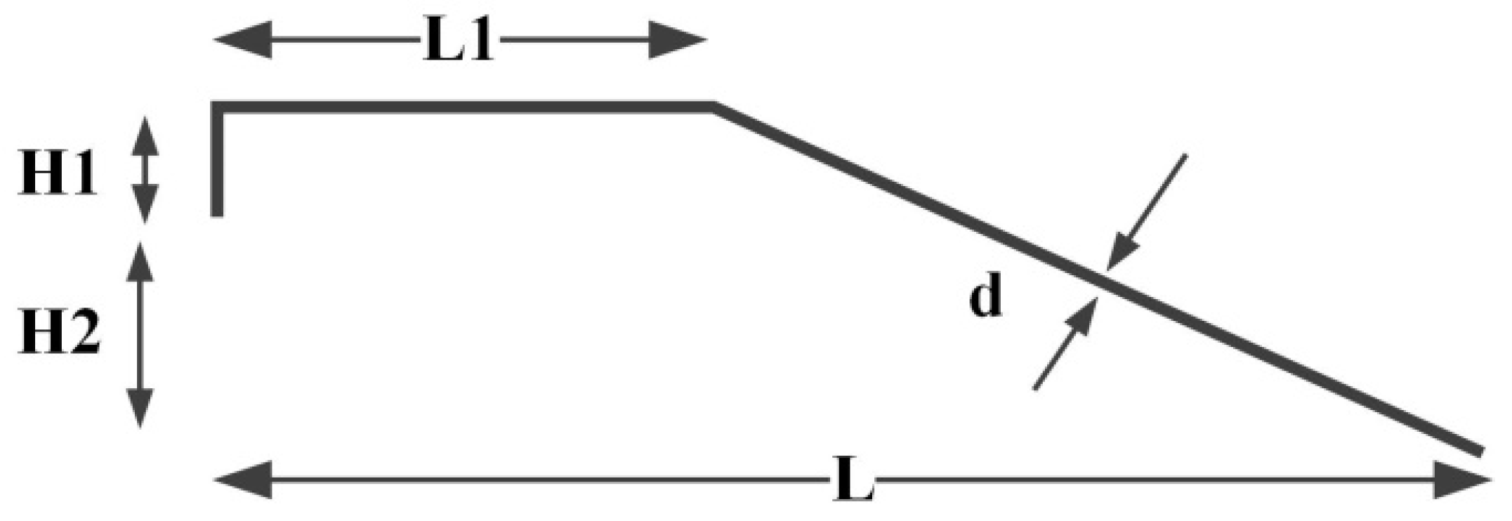
2.1. Geometric Parameters
2.2. Simulation Model of Single Gold Bonding Wire
2.3. Solve Setting
3. Frequency Domain Simulation
3.1. Influence of Flat Length Ratio on S Parameter of Bonding Wire
3.2. Influence of Diameter on S Parameter of Bonding Wire
3.3. Influence of Span on S Parameter of Bonding Wire
3.4. Influence of Bonding Height on S Parameter of Bonding Wire
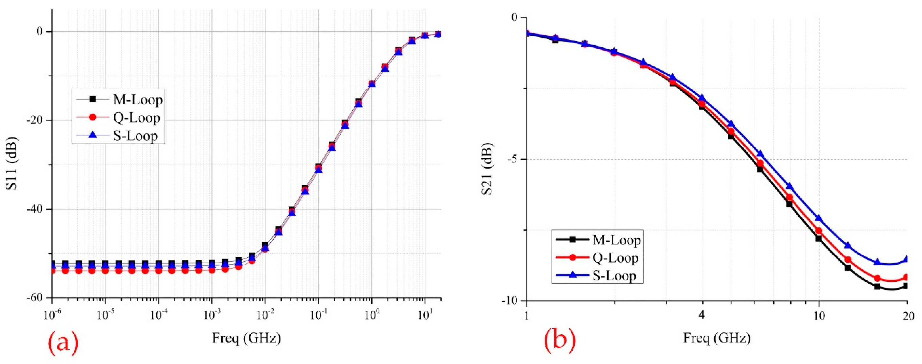
3.5. Influence Of Three Loops On S Parameter Of Bonding Wire
3.6. Design Rules
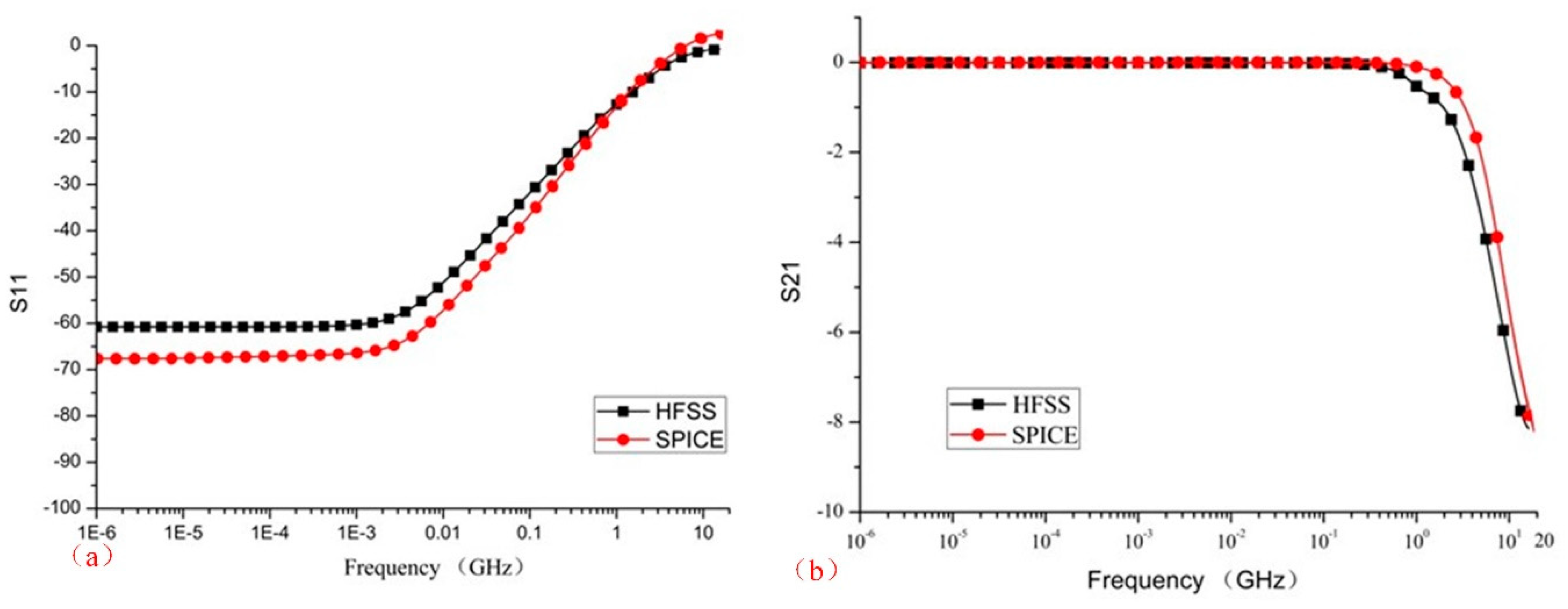
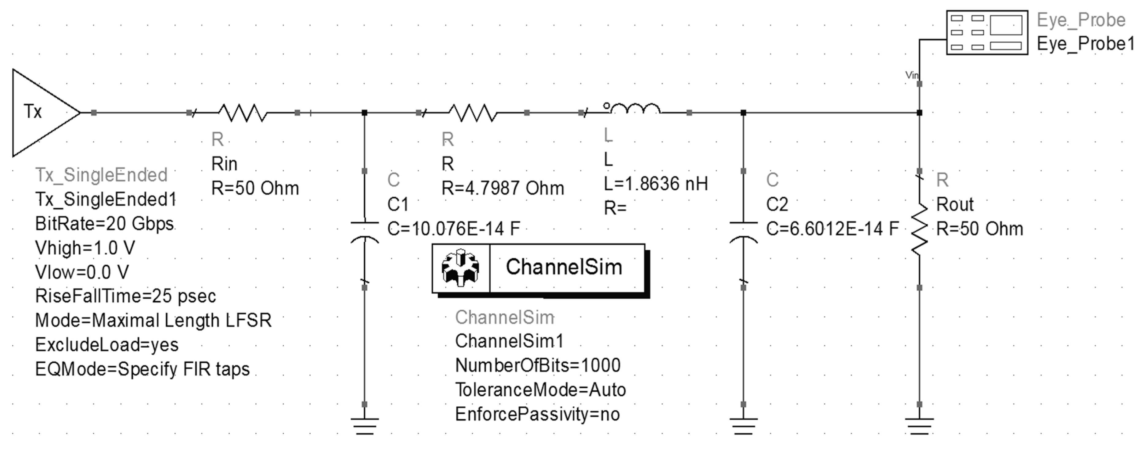
3.7. SPICE Equivalent Circuit Model Of Bonding Wire
3.8. Eye Diagram Analysis
4. Bonding Wire Design and Measurement Experiment
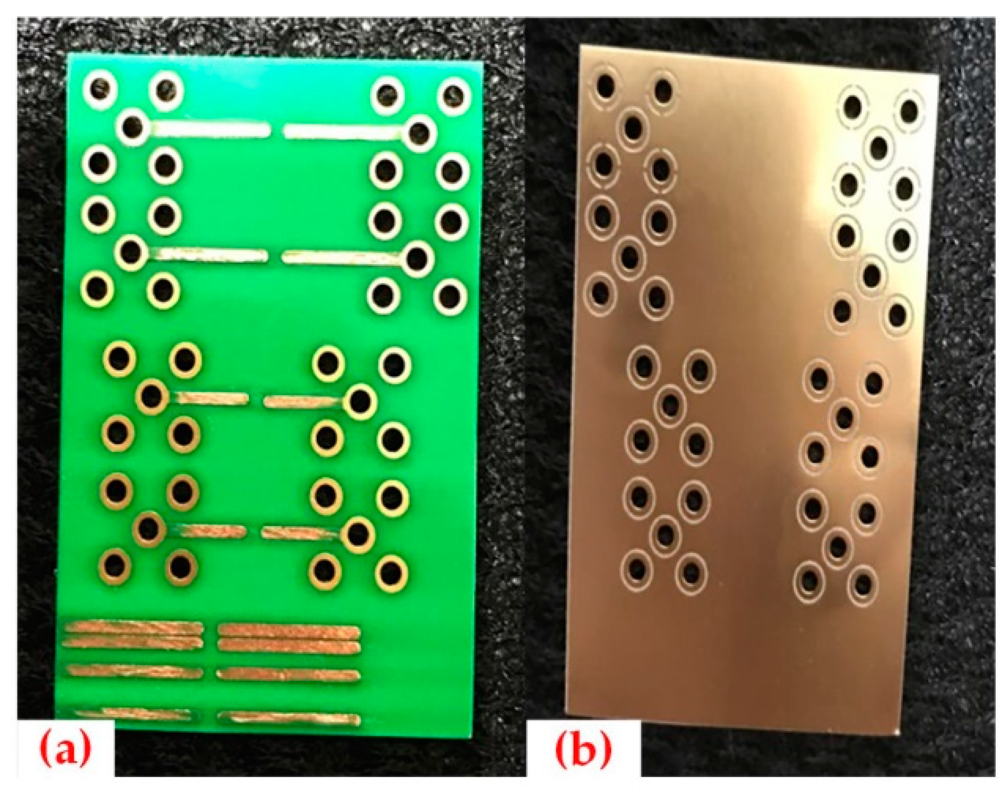
4.1. Circuit Board Design
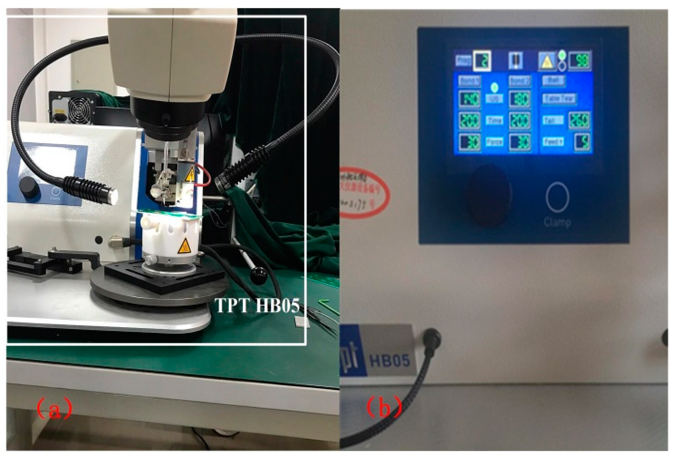
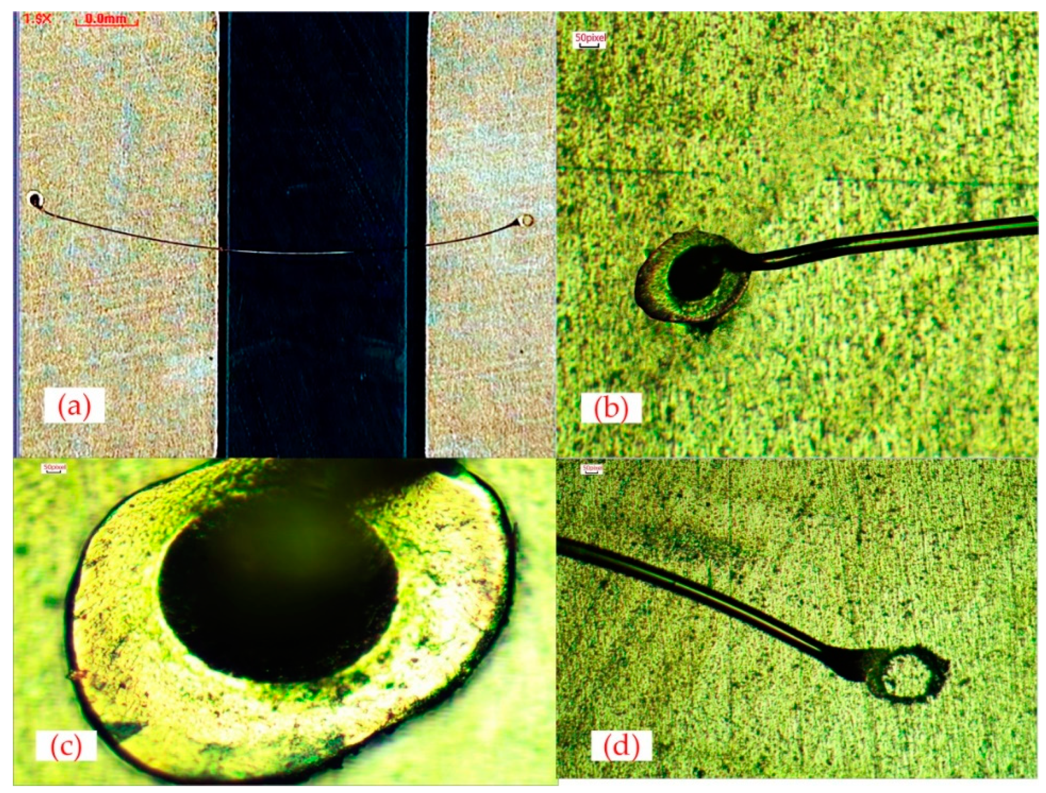
4.2. Bonding Wire Shape
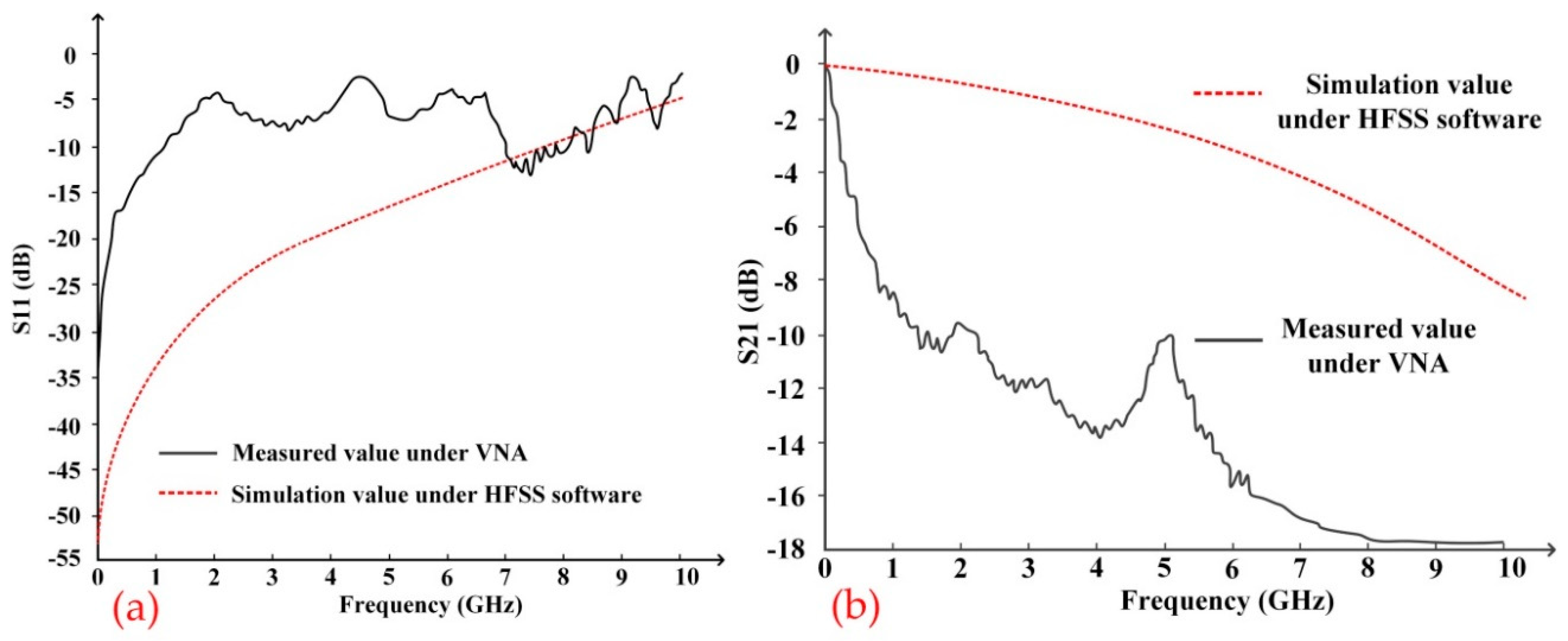
4.3. S Parameter Measurement And Error Analysis
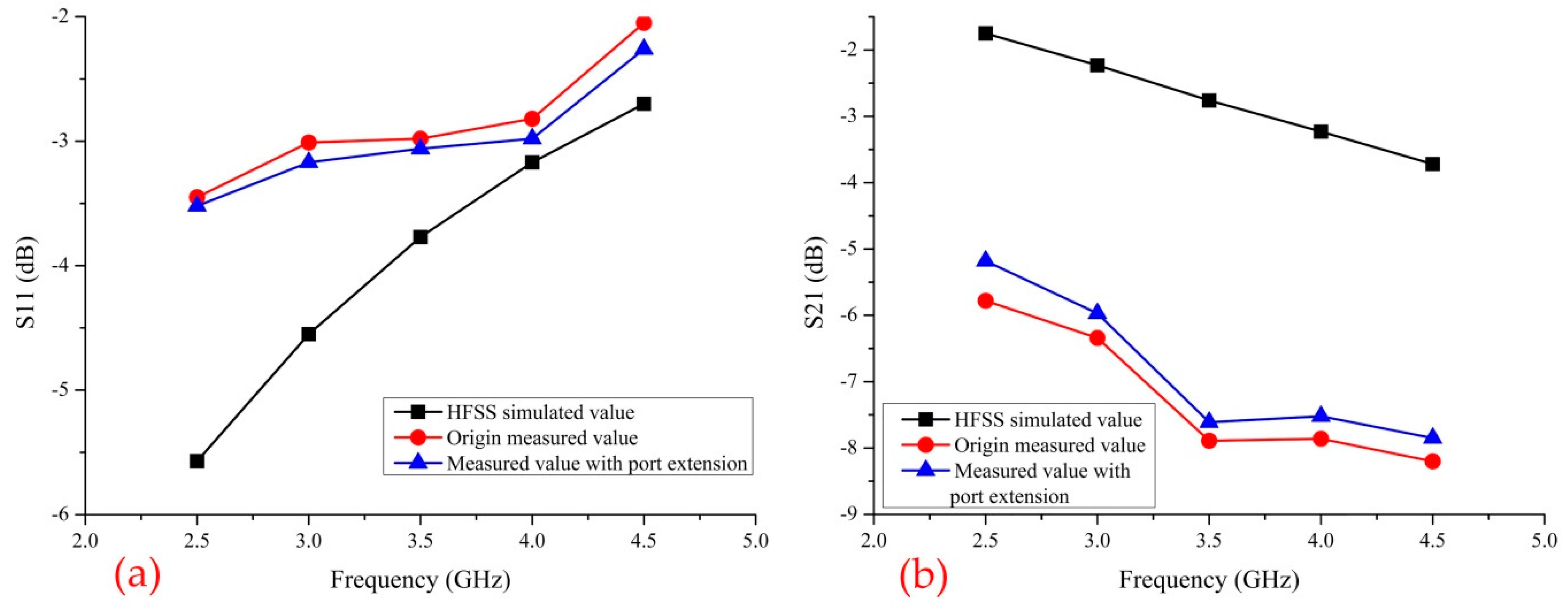
4.4. Port Extension
5. Conclusions
Author Contributions
Acknowledgments
Conflicts of Interest
References
- Fischer, A.C.; Korvink, J.G.; Roxhed, N. Unconventional applications of wire bonding create opportunities for microsystem integration. J. Micromechan. Microeng. 2013, 23, 905–923. [Google Scholar] [CrossRef]
- Chao, Y.Q.; Yang, Z.J.; Qiao, H.L. Progress on Technology of Wire Bonding. J. Electron. Process Technol. 2007, 4, 205–210. [Google Scholar]
- Tian, W. Electronic Packaging, Microelectromechanical and Micro System; Xidian University Press: Xi’an, China, 2012; Volume 1, pp. 59–66. [Google Scholar]
- Casper, T. Electrothermal simulation of bonding wire degradation under uncertain geometries. In Proceedings of the Automation & Test in Europe Conference & Exhibition, Dresden, Germany, 14–18 March 2016. [Google Scholar]
- Manoharan, S.; Patel, C.; Mccluskey, P.; Pecht, M. Effective decapsulation of copper wire-bonded microelectronic devices for reliability assessment. Microelectron. Reliab. 2018, 84, 197–207. [Google Scholar] [CrossRef]
- Ke, M.; Li, D.; Dai, X.; Jiang, H.; Deviny, I.; Luo, H.; Liu, G. Improved surge current capability of power diode with copper metallization and heavy copper wire bonding. In Proceedings of the IEEE European Conference on Power Electronics & Applications, Karlsruhe, Germany, 5–9 September 2016. [Google Scholar]
- Lorenz, G.; Naumann, F.; Mittag, M.; Petzold, M. In Mechanical characterization of bond wire materials in electronic devices at elevated temperatures. In Proceedings of the IEEE 5th Electronics System-integration Technology Conference (ESTC), Helsinki, Finland, 16–18 September 2014; pp. 1–6. [Google Scholar]
- Zhong, Z.W. Overview of wire bonding using copper wire or insulated wire. Microelectron. Reliab. 2011, 51, 4–12. [Google Scholar] [CrossRef]
- Liu, P.; Tong, L.; Wang, J.; Shi, L.; Tang, H. Challenges and developments of copper wire bonding technology. Microelectron. Reliab. 2012, 52, 1092–1098. [Google Scholar] [CrossRef]
- Ndip, I.; Huhn, M.; Brandenburger, F.; Ehrhardt, C.; Schneider-Ramelow, M.; Reichl, H.; Lang, K.D.; Henke, H. Experimental verification and analysis of analytical model of the shape of bond wire antennas. Electron. Lett. 2017, 53, 906–908. [Google Scholar] [CrossRef]
- Zuo, P.; Wang, M.; Li, H.; Song, T.; Liu, J.; Li, E.P. Modeling and analysis of transmission performance of bonding wire interconnection. In Proceedings of the IEEE MTT-S International Conference on Numerical Electromagnetic & Multiphysics Modeling & Optimization, Beijing, China, 27–29 July 2016. [Google Scholar]
- Yu, X.Q.; Bai, Y.D.; Zhou, Y.; Bai, W.; Yang, L.; Min, J.X. In EMI study of high-speed IC package based on pin map. In Proceedings of the IEEE Asia-Pacific International Symposium on Electromagnetic Compatibility, New York, NY, USA, 21–24 May 2012; pp. 305–308. [Google Scholar]
- Huang, N.K.H.; Jiang, L.J.; Yu, H.C.; Li, G.; Xu, S.; Ren, H.S. Fundamental components of the IC packaging electromagnetic interference (EMI) analysis. In Proceedings of the IEEE 21st Conference on Electrical Performance of Electronic Packaging and Systems, New York, NY, USA, 21–24 October 2012; pp. 141–144. [Google Scholar]
- Lim, J.H.; Kwon, D.H.; Rieh, J.S.; Kim, S.W.; Hwang, S.W. RF characterization and modeling of various wire bond transitions. IEEE Trans. Adv. Packag. 2005, 28, 772–778. [Google Scholar]
- Radojcic, R.; Chandrasekaran, A.; Lane, R. Hybrid Package Construction with Wire Bond and through Silicon Vias. U.S. Patent No. 8,803,305, 12 August 2014. [Google Scholar]
- Zhang, Y. Study on Influence of Grounding Vias Substrate on Performance of Millimeter Wave Products. J. Radio Eng. 2017, 47, 60–63. [Google Scholar]
- Lu, F.; Cao, Y.; Lian, B. Study on the electrical performance of one differential pair bonding fingers on different layers in wire bonding package. In Proceedings of the IEEE International Conference on Electronic Packaging Technology, Wuhan, China, 16–19 August 2016. [Google Scholar]
- Liang, Y.; Huang, C.; Wang, W. Modeling and characterization of the bonding-wire interconnection for microwave. In Proceedings of the IEEE MCM International Conference on Electronic Packaging Technology & High Density Packaging, Xi’an, China, 16–19 August 2010. [Google Scholar]
- Kung, H.K.; Chen, H.S.; Lu, M.C. The wire sag problem in wire bonding technology for semiconductor packaging. Microelectron. Reliab. 2013, 53, 288–296. [Google Scholar] [CrossRef]
- Liu, G.M. Dielectric Resonator Antenna Research. Master’s Thesis, Zhejiang University, Hangzhou, China, 2005. [Google Scholar]

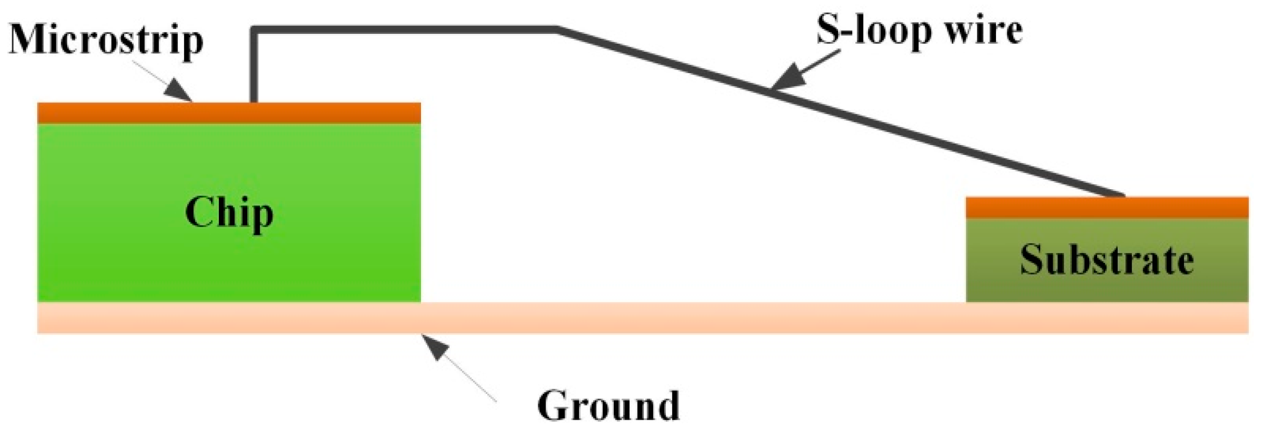









| Name | Material | Dielectric Constant |
|---|---|---|
| S-loop wire | Gold | 0.99996 |
| Microstrip | Copper | 0.99991 |
| Chip | Silicon | 11.9 |
| Substrate | Rogers RO4350B | 3.66 |
| Ground | Copper | 0.99991 |
| Ratio of Flat Length to Span | SP00 | SP12 | SP20 | SP40 | SP60 | SP70 |
|---|---|---|---|---|---|---|
| Min S21 (Insertion Loss)/dB | −9.10 | −8.71 | −9.34 | −9.58 | −9.82 | −9.92 |
| Corresponding frequency/GHz | 17.63 | 17.38 | 17.58 | 17.58 | 17.48 | 17.48 |
| Passing signal/incoming signal/% | 35.07 | 36.69 | 34.12 | 33.19 | 32.28 | 31.92 |
| Diameter/μm | 15 | 20 | 25 | 30 | 35 | 40 |
|---|---|---|---|---|---|---|
| Min S21 (Insertion Loss)/dB | −9.42 | −8.87 | −8.71 | −8.55 | −8.37 | −8.16 |
| Corresponding frequency/GHz | 17.53 | 17.43 | 17.38 | 17.38 | 17.33 | 17.18 |
| Passing signal/incoming signal/% | 33.80 | 36.01 | 36.67 | 37.38 | 38.16 | 39.06 |
| Span/μm | 2500 | 3000 | 3500 | 4000 | 4500 | 5000 |
|---|---|---|---|---|---|---|
| Min S21 (Insertion Loss)/dB | −8.01 | −8.37 | −8.69 | −8.71 | −8.96 | −9.03 |
| Corresponding frequency/GHz | 25.12 | 22.54 | 19.82 | 17.33 | 15.67 | 14.33 |
| Passing signal/incoming signal/% | 39.76 | 38.15 | 36.77 | 36.69 | 35.65 | 35.36 |
| Bonding Height/μm | 210 | 230 | 250 | 270 | 290 | 310 |
|---|---|---|---|---|---|---|
| Min S21 (Insertion Loss)/dB | −8.61 | −8.59 | −8.71 | −8.79 | −8.88 | −9.02 |
| Corresponding frequency/GHz | 17.58 | 17.33 | 17.38 | 17.28 | 17.43 | 17.38 |
| Passing signal/incoming signal/% | 37.11 | 37.20 | 36.69 | 36.35 | 35.97 | 35.40 |
| Bonding Wire Loop | M | Q | S |
|---|---|---|---|
| Min S21 (Insertion Loss)/dB | −9.59 | −9.29 | −8.71 |
| Corresponding frequency/GHz | 17.73 | 17.68 | 17.38 |
| Passing signal/incoming signal/% | 33.15 | 34.32 | 36.69 |
| Factors | Measurement | Restriction |
|---|---|---|
| Flat Length (S-loop wire) | Flat length changes nonlinearly with return loss and insertion loss. The flat length only stands in a specific value, and its signal transmission performance is good | Through the comparison of the data, it is found that signal quality is the best when the flat ratio of length and span is 12%, maybe the best L1/L is 11% or 13% in real operation. |
| Diameter | The bigger diameter is, the better electrical properties are. Insertion loss and equivalent inductance decline with increasing diameter. | Excessive increase in wire diameter: 1. Aggravate the cost of materials 2. Decline in toughness |
| Span | The shorter loop span is, the better electrical properties are. Shorter loop can reduce signal loss and improve the quality of signal transmission. | Too shorter span: 1. Increase line tension, 2. Make welding spot unstable 3. Cause wire sag and sweep problem |
| Bonding Height | The lower wire height is, the better electrical properties are. | Too lower height: 1. Stress concentration 2. Phenomenon of expanding under hot condition and shrinking under cold condition in bonded component. |
| Number | Span/μm | Logical 1 Voltage/V | Logical 0 Voltage/V | Eye Height/V | Eye Width/ps |
|---|---|---|---|---|---|
| a | 2000 | 0.473 | 0.012 | 0.424 | 50 |
| b | 2500 | 0.458 | 0.021 | 0.392 | 50 |
| c | 3000 | 0.450 | 0.028 | 0.351 | 49.5 |
| d | 3500 | 0.441 | 0.032 | 0.320 | 49.25 |
| e | 4000 | 0.440 | 0.039 | 0.294 | 48.75 |
| f | 4500 | 0.425 | 0.046 | 0.261 | 48 |
| Frequency/GHz | ||||
| 2.5 | 6.67 × 10⁻¹ | −2.51 × 10 | 5.51 × 10⁻² | 3.27 × 10 |
| 3.0 | 6.94 × 10⁻¹ | 5.87 × 10 | 5.03 × 10⁻² | −4.62 × 10 |
| 3.5 | 7.03 × 10⁻¹ | 2.60 × 10² | 4.16 × 10⁻² | −8.54 × 10 |
| 4.0 | 7.10 × 10⁻¹ | −4.21 × 10 | 4.21 × 10⁻² | −1.08 × 10 |
| 4.5 | 7.71 × 10⁻¹ | 8.59 × 10 | 4.05 × 10⁻² | 1.85 × 10² |
| Frequency/GHz | ||||
| 2.5 | 4.65 × 10⁻² | 3.24 × 10 | 6.89× 10⁻¹ | −2.69 × 10 |
| 3.0 | 4.47 × 10⁻² | −2.89 × 10 | 7.23 × 10⁻¹ | 4.17 × 10 |
| 3.5 | 4.32 × 10⁻² | −5.69 × 10 | 7.42 × 10⁻¹ | 3.28× 10² |
| 4.0 | 4.02 × 10⁻² | −6.78 × 10² | 7.38 × 10⁻¹ | −8.26 × 10 |
| 4.5 | 3.65 × 10⁻² | 1.95 × 10² | 7.94 × 10⁻¹ | 1.22 × 10 |
| S Parameter | Max Relative Error | Frequency | Min Relative Error | Frequency |
|---|---|---|---|---|
| S11 | 33% | 2.5 GHz | 11% | 4.0 GHz |
| S21 | 69% | 3.5 GHz | 39% | 2.5 GHz |
© 2019 by the authors. Licensee MDPI, Basel, Switzerland. This article is an open access article distributed under the terms and conditions of the Creative Commons Attribution (CC BY) license (http://creativecommons.org/licenses/by/4.0/).
Share and Cite
Tian, W.; Cui, H.; Yu, W. Analysis and Experimental Test of Electrical Characteristics on Bonding Wire. Electronics 2019, 8, 365. https://doi.org/10.3390/electronics8030365
Tian W, Cui H, Yu W. Analysis and Experimental Test of Electrical Characteristics on Bonding Wire. Electronics. 2019; 8(3):365. https://doi.org/10.3390/electronics8030365
Chicago/Turabian StyleTian, Wenchao, Hao Cui, and Wenbo Yu. 2019. "Analysis and Experimental Test of Electrical Characteristics on Bonding Wire" Electronics 8, no. 3: 365. https://doi.org/10.3390/electronics8030365
APA StyleTian, W., Cui, H., & Yu, W. (2019). Analysis and Experimental Test of Electrical Characteristics on Bonding Wire. Electronics, 8(3), 365. https://doi.org/10.3390/electronics8030365


