Article

A High-Efficiency K-band MMIC Linear Amplifier Using Diode Compensation

School of Aeronautics and Astronautics, Zhejiang University, Hangzhou 310027, China
*
Author to whom correspondence should be addressed.
Electronics 2019, 8(5), 487; https://doi.org/10.3390/electronics8050487
Submission received: 12 April 2019 / Revised: 28 April 2019 / Accepted: 29 April 2019 / Published: 30 April 2019
(This article belongs to the Special Issue Millimeter-Wave (mmWave) Communications)

Abstract

:
This paper describes the design and measured performance of a high-efficiency and linearity-enhanced K-band MMIC amplifier fabricated with a 0.15 μm GaAs pHEMT processing technology. The linearization enhancement method utilizing a parallel nonlinear capacitance compensation diode was analyzed and verified. The three-stage MMIC operating at 20–22 GHz obtained an improved third-order intermodulation ratio (IM3) of 20 dBc at a 27 dBm per carrier output power while demonstrating higher than a 27 dB small signal gain and 1-dB compression point output power of 30 dBm with 33% power added efficiency (PAE). The chip dimension was 2.00 mm × 1.40 mm.

1. Introduction

GaAs MMIC is regarded as the premier power device for the microwave communication system [1] and phase array radar system [2] witnessed in recent decades. However, when facing high peak-to-average ratio (PAR) modulation schemes such as QPSK and OFDM, the nonlinearity of the power amplifier causes spectral reproduction and intermodulation distortion. When multi-signals are amplified within a single channel, the beat between carriers generates amplitude modulation [3].
To meet the linearity requirements in the point-to-point radio or satellite communications which usually operate with a high PAR and inconstant enveloped input signal, conventional designs have to work at a back-off output point compared to their saturated power level. Thus, several techniques have been employed to improve the efficiency in the low power region, such as the linear Doherty design, feed-forward technique, and envelop feedback. Some linear Doherty amplifier [4] and feed-forward designs [5] show a high linearity at an acceptable efficiency; however the complexity and cost of chips are not low. Class-J [6] was also reported to achieve a high linearity in the back-off region. Those technologies usually generate a high circuit complexity. Some literature has also reported on the possibility of inner chip nonlinear compensation methods based on diodes [7]. However, no concrete MMIC design has been proposed.
This paper presents a high-efficiency K-band MMIC linear power amplifier fabricated with a 0.15 μm GaAs pHEMT processing technology. A kind of linearizer circuit of diode nonlinear compensation was accomplished. The Y-parameter matrix method was used to analyze and deduce the dynamic characteristic of the parallel diode and FET network. Both simulation and measurement results show the linearity improvement of the circuit. As a result, the proposed linear amplifier achieved an excellent performance with more than a 1 W output power and 33% power-added efficiency at the 1-dB compression point while maintaining an IM3 better than 20 dBc at an output power of 27 dBm per carrier over a 20–22 GHz band.

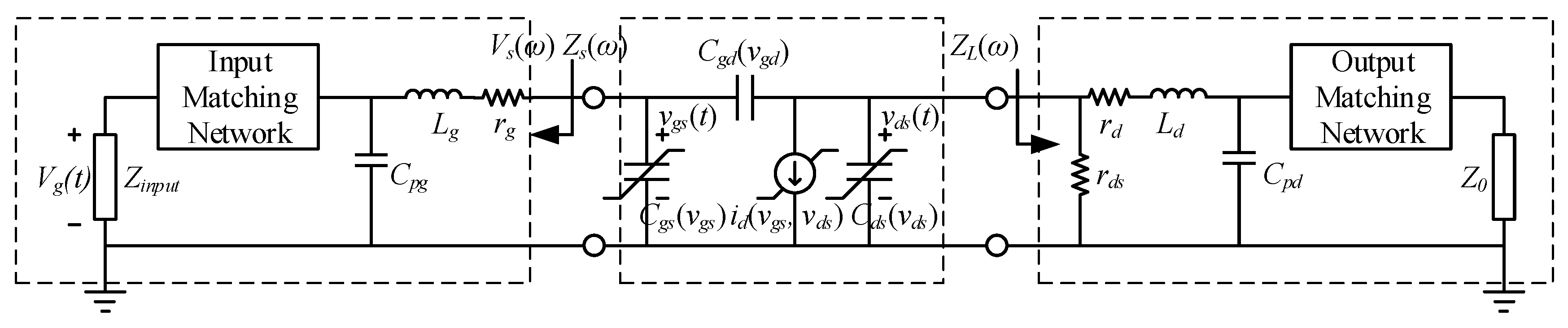
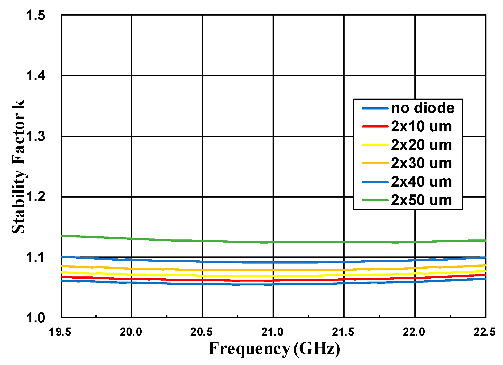
2. Nonlinear Analysis and Diode Compensation

Table 1 shows the main parameter of the 0.15 μm GaAs pHEMT process. The equivalent circuit models of pHEMT and a diode are shown in Figure 1.
Using a diode depletion capacitance model [8], the values of Cgs and Cgd can be derived as
C g s ( v g s ) = C g s b 1 v g s v b i
C g d ( v g d ) = C g d b 1 v g d v b i
The functional model of a single-stage pHEMT amplifier can be represented by Figure 2.
In this model, VS(ω) and ZS(ω) constitute the Thevenin equivalent of the excitation source and the input matching network, and ZL(ω) is the load impedance of the pHEMT. Assuming that the pHEMT is excited by a voltage, vgs(A, t):
v g s ( A , t ) = 0 n V g s k ( A , ω ) cos ( k ω 0 t )
where Vgsk represents the Fourier components of vgs and A is the amplitude. By setting the dynamic charge between the gate and source determined by vgs as Qgs, igs can be derived as
i g s ( t ) = Q g s [ v g s ] t = C g s [ v g s ] v g s t
Then, we get the frequency domain representation of igs as
I g s = [ 1 2 n n C g s k ( V g s , ω ) ] [ 1 2 n n j k ω 0 V g s k ]
where Cgsk is the Fourier components of Cgs:
C g s k = ω 2 π π / ω π / ω C g s [ v g s ] e j k ω 0 t d t
Substituting (R4) into (R3), the fundamental component of igs would be
I g s 1 = j ω 0 C g s 0 V g s 1 + 1 2 j 2 ω 0 C g s 1 * V g s 2 1 2 j ω 0 C g s 2 V g s 1 * +
As a result, the fundamental vgs(t) voltage Vgs1 (A) can be derived as
V g s 1 = V S ( ω ) j ω Z s ( ω ) { C g s 0 V g s 1 + C g s 1 * V g s 2 1 2 C g s 2 V g s 1 * + }
and solving (8) leads to
V g s 1 = V s ( ω ) 1 + j ω Z s ( ω ) C g s 0
The term involving Cgs2 and Vgs2 is neglected as it is significantly smaller than the others. Incorporating the feedback capacitor Cgd into (9), we get
V g s 1 = V s ( ω ) 1 + j ω Z s ( ω ) [ C g s 0 + C g d ( 1 A v ) ]
(10) reveals that Cgs and Cgd influence the phase of fundamental vgs(t), which leads to AM/PM distortion. Using a similar method, we can derive the fundamental vds(t) voltage Vds1 (A) as
V d s 1 ( A ) Z L ( ω ) I d 1 ( A ) 1 + j ω Z L ( ω ) [ C d s 0 ( A ) + C g d ( A v 1 A v ) ]
The term involving Cds2 is neglected as it is significantly smaller than the others. Since the denominator of (11) is approximately equal to unity [9], as a result, there is no significant impact on AM/PM brought about by Cds. From (10) and (11), it can be derived that the main contributors to the AM/PM distortion are the variations of Cgs and Cgd. According to the barrier capacitance effect, the value of Cgs is usually much bigger than that of Cgd. Therefore, the nonlinear characteristic of pHEMT is mainly contributed by Cgs, which approximately equals Cin. As shown in Figure 3, a Schottky diode is parallel in the gate and the drain of the output stage FET to compensate for the nonlinearity of Cgs.
The voltage between the reverse diode is
v d i o d e = v d s v g s
The two-port Y-parameter matrix can be utilized to analyse the parallel network composed of the FET and diode. The matrix form of FET is as follows:
[ i g i d ] = [ y 11 y 12 y 21 y 22 ] [ v g s v d s ]
where
y 11 = j ω C g s 1 + j ω C g s r g s + j ω C g d
y 12 = j ω C g d
y 21 = g m 1 + j ω C g s R g s j ω C g d
y 22 = 1 r d s + j ω ( C d s + C g s )
Incorporating the diode barrier capacitance into the matrix,
y 11 = j ω C g s 1 + j ω C g s r g s + j ω ( C g d + C d i o d e )
C i n = 1 ω Im ( 1 y 11 )
Cin′ represents the input capacitance of the network. According to the previous analysis, the state of input capacitance mainly determines the nonlinear characteristics of the network. Thus, it is possible to perform distortion compensation utilizing the high-frequency C-V characteristic of the diode. As vdiode < 0, Cdiode is dominated by depletion layer capacitance Cj, where
C j = C j 0 1 v d i o d e Φ B
where ΦB is the junction built-in potential, so
C i n = [ ω C g s R g s ( C g d + C j ) ] 2 + ( C g s + C g d + C j ) 2 ( ω C g s R g s ) 2 ( C g d + C j ) ( C g s + C g d + C j )
As the input RF power increases, the electric field within the FET channel is enhanced, which makes the swing of both vgs and vds become higher. However, the negative swing of vds is limited by the knee voltage (Vknee) and the positive swing of vgs is limited by the diffusion barrier voltage (Vdiff). As a result, v ¯ ds grows higher while v ¯ gs grows lower. Consequently, v ¯ diode (3) becomes higher while v ¯ gs becomes lower. The voltage waveform versus input RF power is shown in Figure 4.
Therefore, substituting (1), (2), and (20) into (21) and combining the voltage analysis above, the characteristics of input capacitance can be shown as the curve in Figure 5.
The principles for the choice of diode periphery are as follows.
  • The size of the diode should be large enough to compensate for the input capacitance of the pHEMT as the input power increases;
  • The barrier capacitance of the diode should not be too large to over change the input characteristics of the HMET and generate excessive feedback between drain and gate.
Figure 6 shows that as the size of diode increases, the additional feedback becomes stronger. As a result, the MaxGain of the network decreases, which leads to lower linear gain. Therefore, combined with the C-V characteristics of the diode shown in Figure 5a, we gradually adjusted the diode size so that it could effectively compensate for the input capacitance of pHEMT while reducing the effect on the gain. The C-V characteristics of the selected 2 × 20 μm diode and the input capacitance of the network versus RF power are shown in Figure 7.
The parasitic parameter value of the selected pHEMT and diode is shown in Table 2 and Table 3, respectively.
Converting (7) to the S-parameter matrix:
[ b 1 b 2 ] = [ S 11 S 12 S 21 S 22 ] [ a 1 a 2 ]
where
S 11 = ( 1 Z 0 y 11 ) ( 1 + Z 0 y 22 ) + y 12 y 21 Z 0 2 Ψ
S 12 = 2 Y 12 Z 0 Ψ
S 21 = 2 Y 21 Z 0 Ψ
S 22 = ( 1 + Z 0 y 11 ) ( 1 Z 0 y 22 ) + y 12 y 21 Z 0 2 Ψ
Ψ = ( 1 + Z 0 y 11 ) ( 1 + Z 0 y 22 ) y 12 y 21 Z 0 2
Using the S-parameter to derive the stability factor of the network:
k = 1 | S 11 | 2 | S 22 | 2 + | Δ | 2 2 | S 12 | | S 21 |
Δ = S 11 S 22 S 12 S 21
The factor k > 1 is a necessary and sufficient condition for network stability. Since the diode compensation method generates additional feedback between the gate and drain, the stability of the network is enhanced compared with single FET. The conclusion can be verified by calculation or simulation. The simulation result of the stability factor is shown in Figure 8.
Consequently, because of the nonlinear effect of the diodes, the input capacitance of the network is compensated for as the input power increases, thus avoiding the degradation of linearity. As the diode is operated in an inverted connection, there is nearly no additional current or power loss in the circuit.

3. Circuit Design

The K-band MMIC linear amplifier is composed of three-stage FETs fabricated with a 0.15 μm gate length AlGaAs/GaAs pHEMT technology. The process exhibits a gate-drain breakdown voltage of 16.5 V and a cutoff frequency (fT) of 90 GHz. The FETs for the power stage are 8 × 100 μm. Source-pull and load-pull simulations using a large signal model at a center frequency were taken to determine the optimal input and output impedances that lead to a higher output power and efficiency. The output matching network combining two FETs matches the fundamental load impedance based on the load-pull simulation. The interstage and input matching networks are designed to match the conjugated impedance and were optimized for low loss. The circuit of the amplifier configuration is shown in Figure 9. The simulation result of the amplifier is shown in Figure 10 and Figure 11.
Figure 10 and Figure 11 show the improvement of the amplifier linearity performance generated by the parallel diode circuit design.

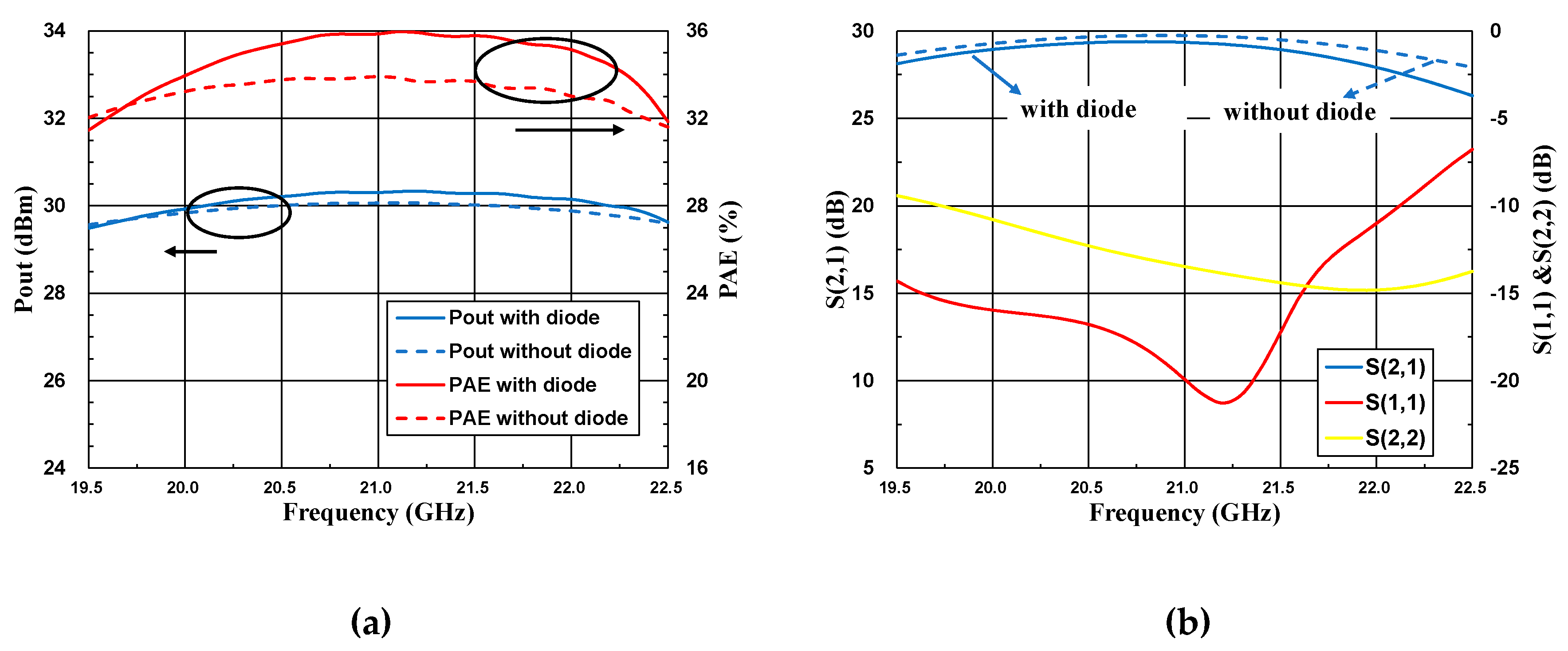
4. Measurement Results

The fabricated three-stage K-band linear amplifier MMIC is shown in Figure 12. The MMIC size is as small as 2.00 × 1.40 mm2 with a GaAs substrate thickness of 50 μm. Linear S-parameter and large signal measurements were performed at a drain voltage of 5 V and gate voltage of −0.8V on a wafer. Figure 13 shows the measured S-parameter of the MMIC from 19.5 GHz to 22.5 GHz. The design has achieved higher than a 26 dB small signal gain and better than a 10 dB input return loss. Figure 14 illustrates the measured output power and PAE for the amplifier at fixed input drive levels of +3.5 dBm under a continuous wave (CW). At the nominal supply of VD = 5 V and VG = −0.8 V, the amplifier demonstrates higher than 30 dBm P1dB with 33–35% PAE over a 20–22 GHz frequency. Very flat power and gain characteristics were achieved for this design. Further PAE improvement should be possible with a more precise power match by the result of a load-pull test.
Two-tone measurement of the amplifier has been performed with 10 MHz tone spacing under the drain voltage of 5 V and gate voltage of −0.8 V. The intermodulation distortion was measured on a wafer with 10 MHz two-tone spacing. The two carrier sources were connected to the chip through a power combiner with an isolator in order to reduce the intermodulation contributions of the setup. As shown in Figure 15, IMD3 better than 20 dBc and PAE higher than 33% were measured at an output power of 27 dBm per carrier over a 20–22 GHz band. Compared to the design without an inner paralleled diode configuration, there is more than a 5dB improvement of IMD3. Table 4 summarizes the performance comparison of this work with other published linear amplifiers working in close frequency ranges. The characteristics of the amplifier, including power, gain, efficiency, and IMD3, are better than the previously reported ones.

5. Conclusions

In this paper, a three-stage K-band 20–22 GHz high-efficiency linear MMIC power amplifier using 0.15 μm GaAs pHEMT technology is reported. The design utilizes an optimum paralleled diode circuit for inner chip linear compensation. The MMIC generates an output power of 30 dBm and PAE of 33% at −1 dB gain compression under CW operation and delivers a lower than −20 dBc IMD3 performance with 10 MHz tone spacing. The MMIC has a smaller size and more than a 5dB improvement of IMD3 was observed.

Author Contributions

Methodology, H.Z.; Software, J.H.; Validation, J.H.; Data Curation, H.Z.; Writing: Original Draft Preparation, H.Z.; Writing: Review and Editing, W.C.; Supervision, W.C.; Project Administration, Z.W.; Funding Acquisition, F.Y.

Funding

This research was funded by the National Natural Science Foundation of China grant number 61604128 and the Fundamental Research Funds for the Central Universities grant number 2017QN81002.

Acknowledgments

The authors would like to thank the Institute of Aerospace Electronics Engineering of Zhejiang University for providing the research platform and technical support.

Conflicts of Interest

The authors declare no conflict of interest.

References

  1. Camarchia, V.; Guerrieri, S.D.; Ghione, G.; Pirola, M.; Quaglia, R.; Rubio, J.M.; Loran, B.; Palomba, F.; Sivverini, G. A K-band GaAs MMIC Doherty power amplifier for point-to-point microwave backhaul applications. In Proceedings of the 2014 International Workshop on Integrated Nonlinear Microwave and Millimetre-wave Circuits (INMMiC), Leuven, Belgium, 2–4 April 2014. [Google Scholar] [CrossRef]
  2. Lane, A.; Jenkins, J.; Green, C.; Myers, F. S and C band GaAs multifunction MMICs for phased array radar. In Proceedings of the 11th Annual Gallium Arsenide Integrated Circuit (GaAs IC) Symposium, San Diego, CA, USA, 22–25 October 1989; pp. 259–262. [Google Scholar] [CrossRef]
  3. Simons, K.A. The decibel relationships between amplifier distortion products. Proc. IEEE 1970, 58, 1071–1086. [Google Scholar] [CrossRef]
  4. Cho, K.-J.; Kim, W.-J.; Kim, J.-H.; Stapleton, S.P. Linearity optimization of a high power Doherty amplifier based on post-distortion compensation. IEEE Microw. Wireless Compon. Lett. 2005, 15, 748–750. [Google Scholar] [CrossRef]
  5. Roy, M.K. Distortion cancellation performance of miniature delay filters for feed-forward linear power amplifiers. IEEE Trans. Ultrason. Ferroelectr. Freq. Control 2002, 49, 1592–1595. [Google Scholar] [CrossRef]
  6. Wright, P.; Lees, J.; Benedikt, J.; Tasker, P.J.; Cripps, S.C. A methodology for realizing high efficiency class-J in a linear and broadband PA. IEEE Trans. Microw. Theory Techn. 2009, 57, 3196–3204. [Google Scholar] [CrossRef]
  7. Mrunal, A.K.; Shirasgaonkar, M.; Patrikar, R.M. Power amplifier linearization using a diode. In Proceedings of the MELECON 2006–2006 IEEE Mediterranean Electrotechnical Conference, Malaga, Spain, 16–19 May 2006; pp. 173–176. [Google Scholar] [CrossRef]
  8. Wren, M.; Brazil, T.J. The effect of the gate Schottky diode on pHEMT power amplifier performance. In Proceedings of the 2003 High Frequency Postgraduate Student Colloquium, Belfast, Ireland, 8–9 September 2003; pp. 52–55. [Google Scholar] [CrossRef]
  9. Nunes, L.C.; Cabral, P.M.; Pedro, J.C. A Physical Model of Power Amplifiers AM/AM and AM/PM Distortions and Their Internal Relationship. In Proceedings of the 2013 IEEE MTT-S International Microwave Symposium Digest (MTT), Seattle, WA, USA, 2–7 June 2013. [Google Scholar] [CrossRef]
  10. Fersch, T.; Quaglia, R.; Pirola, M.; Camarchia, V.; Ramella, C.; Khoshkholgh, A.J.; Ghione, G.; Weigel, R. Stacked GaAs pHEMTs: design of a K-band power amplifier and experimental characterization of mismatch effects. In Proceedings of the 2015 IEEE MTT-S International Microwave Symposium, Phoenix, AZ, USA, 17–22 May 2015; pp. 1–4. [Google Scholar] [CrossRef]
  11. Koo, B.; Park, C.; Lee, K.A.; Chun, J.H.; Hong, S. A 28-dBm pHEMT Power Amplifier Using Voltage Combiner for K-Band Applications. In Proceedings of the 38th European Microwave Conference, Amsterdam, Netherlands, 27–31 October 2008. [Google Scholar] [CrossRef]
  12. Brown, S.A.; Carroll, J.M. Compact, 1 Watt, power amplifier MMICs for K-band applications. In Proceedings of the GaAs IC Symposium, Seattle, WA, USA, 5–8 November 2000. [Google Scholar]
  13. Bessemoulin, A.; Mcculloch, M.G.; Alexander, A.; Mccann, D.; Mahon, S.J.; Harvey, J.T. Compact K-band watt-level GaAsPHEMT power amplifier MMIC with integrated ESD protection. In Proceedings of the 2006 European Microwave Integrated Circuits Conference, Manchester, UK, 10–13 September 2006. [Google Scholar]
  14. Wang, K.; Yan, Y.; Liang, X. A K-band power amplifier in a 0.15-um GaAs pHEMT process. In Proceedings of the 2018 IEEE MTT-S International Wireless Symposium (IWS), Chengdu, China, 6–10 May 2018; pp. 1–3. [Google Scholar]
Figure 1. (a) The equivalent circuit model of pHEMT; (b) the equivalent circuit model of a diode.
Electronics 08 00487 g001
Figure 2. Single-stage pHEMT amplifier model.
Electronics 08 00487 g002
Figure 3. Paralleled Shottky diode linearizer.
Electronics 08 00487 g003
Figure 4. (a) Voltage waveform of vds; (b) voltage waveform of vgs.
Electronics 08 00487 g004
Figure 5. (a) C-V characteristics of the two-finger diode; (b) input capacitance of the network versus RF power.
Electronics 08 00487 g005
Figure 6. The influence of the diode size on the MaxGain of the network.
Electronics 08 00487 g006
Figure 7. (a) C-V characteristics of the 2 × 20 μm diode; (b) input capacitance of the network versus RF power (Behavior of 2 × 20 μm diode and 8 × 100 μm FET).
Electronics 08 00487 g007
Figure 8. The influence of the diode size on the stability factor of the network.
Electronics 08 00487 g008
Figure 9. Schematic of the MMIC linear amplifier.
Electronics 08 00487 g009
Figure 10. (a) Simulated output power and PAE versus frequency at a 3 dBm input power; (b) simulated S-parameter versus frequency; (c) simulated output power, gain, and PAE versus input power at a 21 GHz frequency; (d) simulated IMD3 and PAE versus output power.
Electronics 08 00487 g010aElectronics 08 00487 g010b
Figure 11. (a) Simulated AM-to-AM versus input power at 21 GHz; (b) simulated AM-to-PM versus input power at 21 GHz.
Electronics 08 00487 g011
Figure 12. Photograph of the fabricated K-band linear amplifier.
Electronics 08 00487 g012
Figure 13. Measured small-signal performance of the amplifier under the bias of VD = 5 V and VG = −0.8 V at 25 Celsius.
Electronics 08 00487 g013
Figure 14. Measured output power and PAE at 1 dB compression.
Electronics 08 00487 g014
Figure 15. Measured IMD3 and PAE versus output power under a two-tone test with different frequencies.
Electronics 08 00487 g015
Table 1. The parameters of the 0.15 μm GaAs pHEMT process.
ParameterValueParameterValue
VTH (V)−1.2ft (GHz)85
VBDG (V)10Gm_Peak (mS/mm)495
Idmax (mA/mm)650Pdensity (W/mm)0.8
Idss (mA/mm)500CMIM (pF/mm2)400
Table 2. The parasitic parameter value of the 8 × 100 μm pHEMT
ParameterValueParameterValue
rg (Ω)1.5Ld (pH)8.5
rd (Ω)1.2Ls (pH)0.7
rs (Ω)0.2Cpg (fF)9.5
Lg (pH)9.5Cpd (fF)17.5
Table 3. The parasitic parameter value of the 2 × 20 μm diode
ParameterValue
rgs (Ω)41.5
Cpg (fF)89.0
Cps (fF)33.5
Lgs (pH)55.0
Table 4. Performance comparison of linear amplifiers.
ReferenceProcessFrequency (GHz)P−1dB (dBm)PAE (%)Gain (dB)IMD3 (dBc)Size (mm2)
[10]0.15 µm GaAs20–2331249.5--
[11]0.25 µm GaAs22.8–23.52815.325-2.52
[12]0.25 µm GaAs18–2731.42714183.91
[13]0.15 µm GaAs17–20283021142.96
[14]0.15 µm GaAs24–28282121154.50
This work0.15 µm GaAs20–22303427202.80

