Article

GA-BP in Thermal Fatigue Failure Prediction of Microelectronic Chips

1
School of Petroleum Engineering, China University of Petroleum (East China), Qingdao 266580, China
2
Department of Engineering Mechanics, China University of Petroleum (East China), Qingdao 266580, China
*
Author to whom correspondence should be addressed.
Electronics 2019, 8(5), 542; https://doi.org/10.3390/electronics8050542
Submission received: 13 April 2019 / Revised: 8 May 2019 / Accepted: 10 May 2019 / Published: 14 May 2019
(This article belongs to the Section Microelectronics)

Abstract

:
A thermal fatigue life prediction model of microelectronic chips based on thermal fatigue tests and solder/substrate interfacial singularity analysis from finite element method (FEM) analysis is established in this paper. To save the calculation of interfacial singular parameters of new chips for life prediction, and improve the accuracy of prediction results in actual applications, a hybrid genetic algorithm–artificial neural network (GA–ANN) strategy is utilized. The proposed algorithm combines the local searching ability of the gradient-based back propagation (BP) strategy with the global searching ability of a genetic algorithm. A series of combinations of the dimensions and thermal mechanical properties of the solder and the corresponding singularity parameters at the failure interface are used to train the proposed GA-BP network. The results of the network, together with the established life prediction model, are used to predict the thermal fatigue lives of new chips. The comparison between the network results and thermal fatigue lives recorded in experiments shows that the GA-BP strategy is a successful prediction technique.

1. Introduction

Microelectronic chips are becoming more popular, because their design in smaller dimensions meets the requirements of semiconductor packaging in terms of high-density and cost-effective performance. The solder layer plays an important role in the mechanical and electric connections of the chip; therefore, its performance, especially the thermomechanical properties of the solder, has become an important factor affecting the reliability of microelectronic chips [1,2,3]. During the service process, the chips are subjected to temperature cycling caused by circuit continuity and ambient temperature changes [4]. Due to the difference in the coefficients of thermal expansion (CTE) of various components, stress and strain always occur and gradually accumulate at the solder joints during temperature cycling. A severe CTE mismatch always results in strong interfacial shear and peeling stresses near the interfacial edges and corners. When the local stress level exceeds the bonding strength of the interface, an interfacial crack will initiate and propagate [5,6,7]. Therefore, it is of practical importance to model these stresses using analytical tools, so that the susceptibility to thermal mechanical failure can be predicted for chips with new geometries and material combinations, without costly trial and error.
No well recognized methodologies on how to quantify the interfacial strength and predict crack initiation and propagation have been established. The traditional method is to apply the fatigue law of the solder material itself directly to the solder joints, but this method is not adequate, since the stresses and strains are singular at the idealized interface edge or corner [8,9,10]. To overcome this concern, Hattori et al. suggested an approach for assessing the interface reliability of plastic IC packages using two stress intensity parameters that characterize the stress distributions near a bonded edge along the interface [11]. Similar approaches have been adopted by Gradin [12], Groth [13], and Reedy and Guess [14]. Generally, at the edge, stresses have the singular form σ = K/r1−λ, from which the stress intensity factor K and singular order λ are used to configure a criterion for fatigue crack initiation or delamination. For various loadings, if this value is larger than a certain threshold value Kc, crack initiation or delamination is assumed to occur. However, such a method is based on the concept of point failure, which may be difficult to observe through physical experiments, and is valid only for cases where the geometric shape of the solder joints and the loading conditions are the same, as this is used to inform the fatigue law [15,16]. That is, the empirical fatigue law may have strong limitations in application. For example, the stress intensity factor at the edge of the interface is always dependent on test conditions, assembly geometry, and the mechanical property of the materials and their interactions, as well as the impact of process parameters [17,18], and the process of obtaining accurate singular field parameters at the interface is also time consuming. To save the calculation of the stress intensity factor at the edge of the interface, soft-computing is a good alternative for handling this complex problem, as it is tolerant of imprecision and uncertainty. To date, various soft-computing methods such as ANN [19,20,21], fuzzy logic [22], genetic programming [23,24,25], and adaptive neuro-fuzzy inference systems [26] have been applied to the fatigue problems of engineering materials and structures.
In this paper, a thermal fatigue law is established to predict the service life of microelectronic chips, based on the concept that the fatigue failure initiates within a characteristic length, rather than one point from the solder/substrate interface. The parameters in the fatigue law are determined according to the thermal fatigue lives of chips from tests and interfacial singularity parameters, such as interfacial stress–strain intensity factors and singular orders, obtained from mechanical thermal FEM analysis under the same testing conditions. An attempt has been made to predict the interfacial singularity parameters and thermal fatigue life by applying GA-BP hybrid programming, in which the GA initiates the weights and improves the convergence of the BP network, and the BP network predicts the interfacial singularity parameters of new chips for thermal life prediction. It is observed that the predicted results are in good agreement with the experimental findings.

2. Thermal Fatigue Life Prediction Model

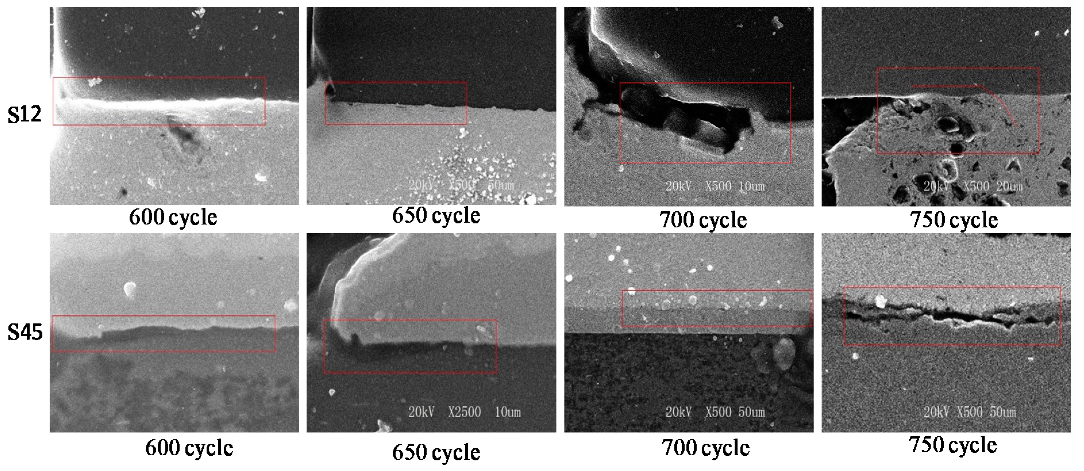
2.1. Thermal Fatigue Tests

The chipset shown in Figure 1 has nineteen pieces of chips, including two pieces of chip Q1, one piece of chip Q2, six pieces of chip Q3, four pieces of chip Q4, and six pieces of chip Q5. The structure of every chip is similar and the specific dimensions of a single chip are shown in Figure 2. The materials shown are the wafer (silicon), solder Pb-5Sn, Cu, solder SnAg3Cu0.5, Cu, insulate layer, substrate, and silica gel. The silica gel protector is cleaned and then the chipset is cut out by a wire cutter. Five types of chips are then put into a same temperature box to undergo cyclic thermal charge, as shown in Figure 3, with a temperature amplitude of 20–150 °C, 20–120 °C and 20–100 °C, respectively.
As the damage or crack in the chip cannot be observed directly, the fatigue life limit has to be defined first. To detect the fatigue failure, the electric resistance of the chips is measured by a digital resistance meter for a certain interval. Figure 4 depicts the typical electric resistance variation of chip Q2 with the thermal cycles (20–150 °C). Figure 5 gives the SEM observation of crack nucleation at the interface of the wafer and solder Pb-5Sn (interface S12), and solder SnAg3Cu0.5 and Cu (interface S45). It is found that the main crack forms first from S45. By comparing the forming of the main crack at S45 and the electronic resistance increase (RI), we define the fatigue life limit Nf by RI reaching 15% [27]. Using this method, we determine the average thermal fatigue lives of five types of chips under different experimental conditions, as listed in Table 1.

2.2. FEM Model

A three dimensional numerical analysis was carried out to obtain a measure of stress and strain under cyclic thermal loading. In this paper, a new segmented constitutive model of the solder is considered. The model consists of two parts: the relationship of strain rate with stress is linear at low stress and has a hyperbolic sine at high stress, as shown in Equation (1). All constants and other material constants in the FEM analysis can be found in the previous work [27].
ε ˙ = { A ( sinh B σ ) n exp ( H / R T ) if σ > σ V A 0 σ exp ( H / R T ) if σ < σ V σ V = C 0 C 1 ( T T R ) + C 2 ( T T R ) 2
where σ is the equivalent stress, σv is the linear viscous creep limit (which is the cross stress between the linear viscous and power-law creep), H is the activation energy, R is the universal gas constant, T is the absolute temperature value, and TR is 273 degrees.
An unsteady thermal conduction analysis and thermal stress analysis were carried out with the corresponding chips. The FEM model of chip Q2 is shown in Figure 6, where the total number of elements is 78,890, the number of nodes is 85,200, and the smallest element size at the interfacial singular zone is 0.00001 mm × 0.00003 mm × 0.00003 mm. The convergence analysis was conducted to ensure the accuracy of our results, as well as the computational efficiency. In the thermal conduction analysis, the surrounding temperature variation is exactly the same as that in the thermal fatigue tests. To express the stress and strain singularity at the edge of the interface between the solder and substrate, specific points at the edges S12 and S45 are selected, as shown in Figure 7. The typical stress and equivalent strain variations with time at point A and B are shown in Figure 8 and Figure 9. The stress near the interfacial edge varies for the first several cycles, but after three cycles it is saturated. The most severe case does not occur at the initial or stable stage, but at the stage of heating. In this case, the normal stress on interface S12 is compressive, and in conclusion, the shear stress is the dominant factor of interface failure. At S45 the maximum traction σt = (σ2 + τ2)1/2 dominates interface failure because the normal stress is tensile.
As the initial condition is set as a zero stress-strain state, the stress and strain ranges are important for fatigue life evaluation. According to the instant singular field theory [28,29]:
σ i = K i ( t ) r δ i ( t ) ,   ε = K ε ( t ) r ς ( t )
where Ki(t) and Kε(t) denote the stress and strain intensity factors, δi(t) and ς(t) are the stress and strain singular orders, and r denotes the distance from the singular edge.
The intensity factors and singular orders of maximum stress and strain at steady state are determined numerically, as shown in Figure 10 and Figure 11. The difference of stress singular orders between the two interfaces is not big, but the stress and strain intensity factors at S45 are larger than that at S12. The singularity of strain is stronger than that of stress, indicating the strain field may be the dominant factor of thermal fatigue failure. As shown with the above methods, the strain singular orders and intensity factors of five types of chips at the maximum state are determined and listed in Table 2.

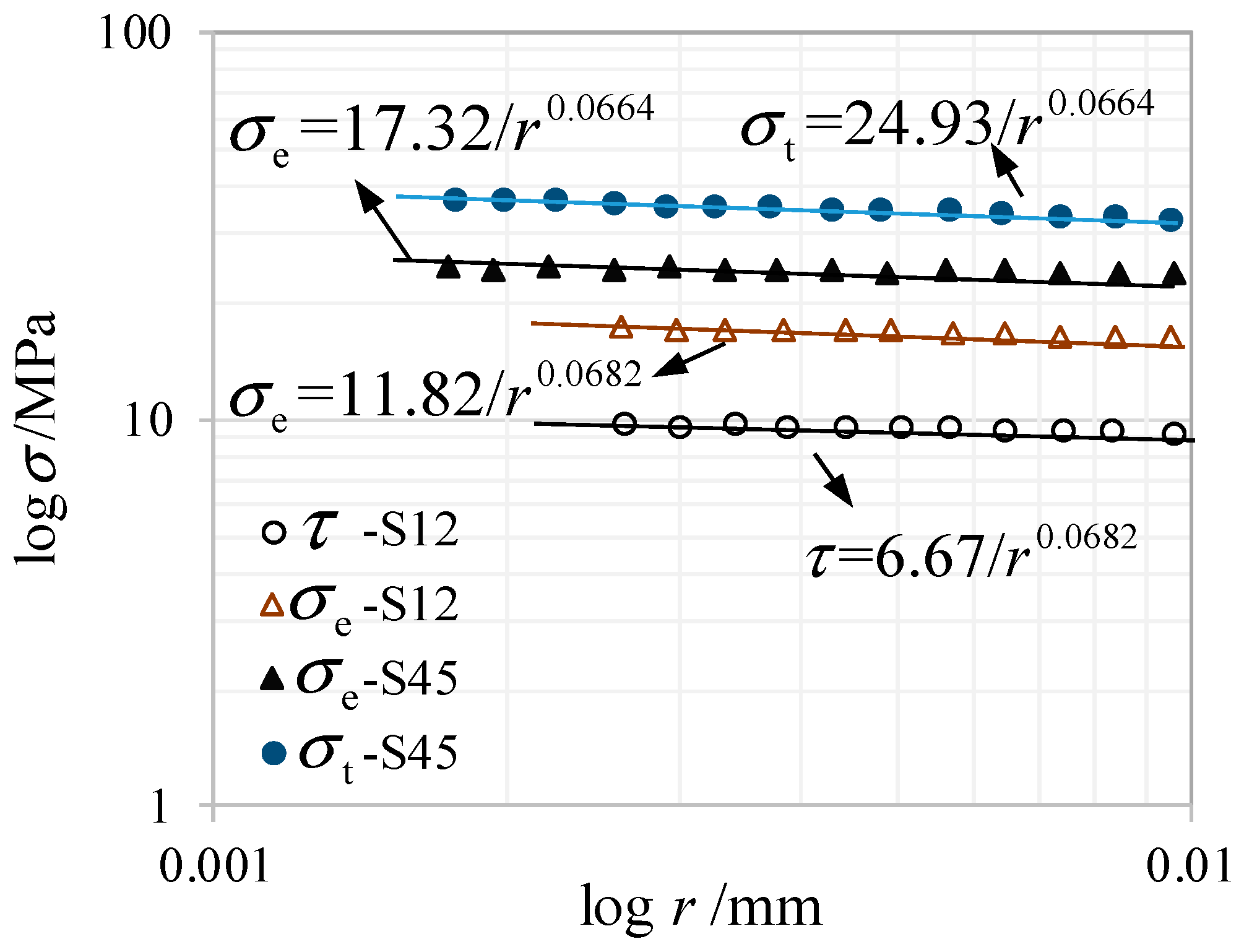
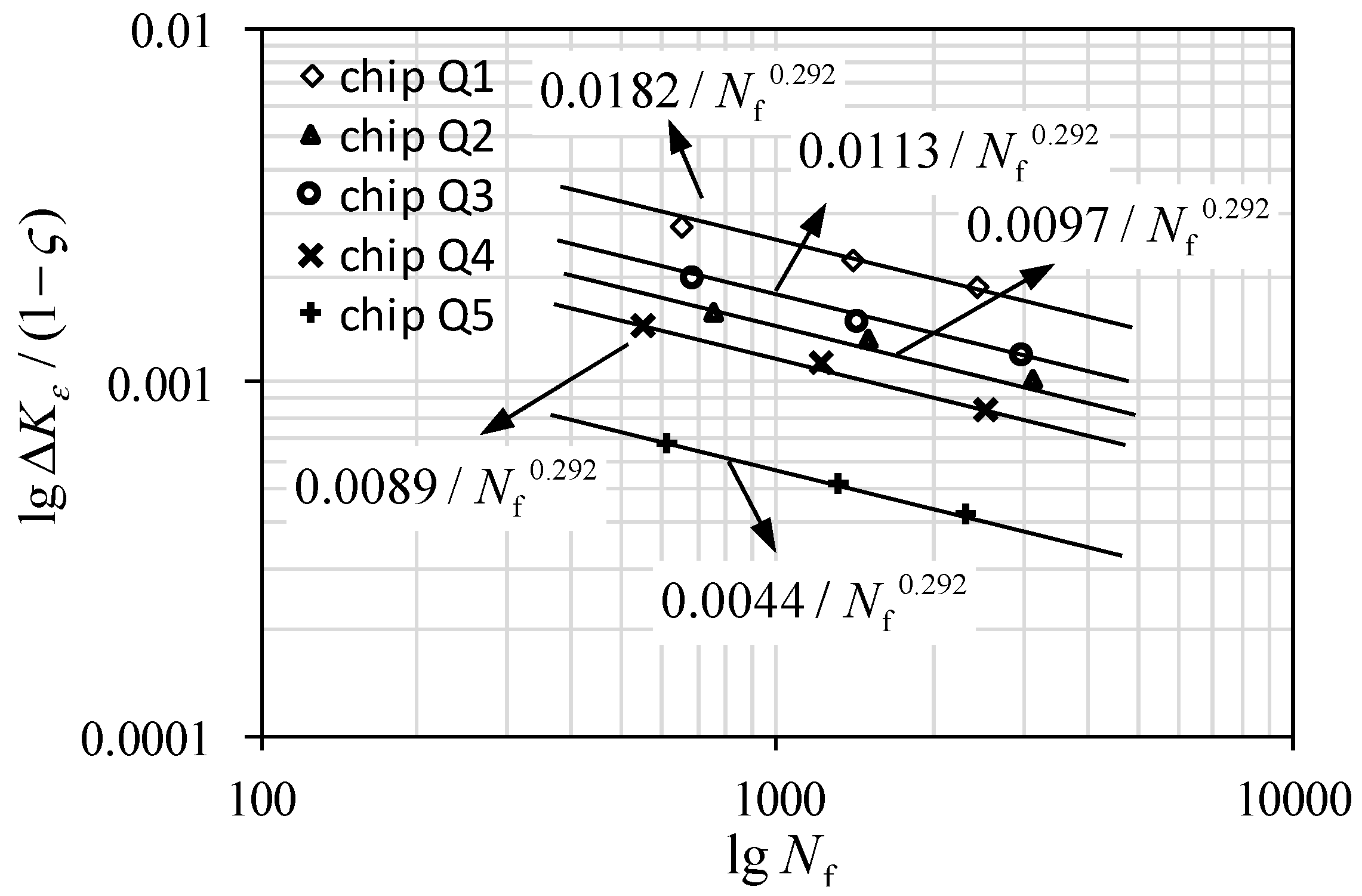
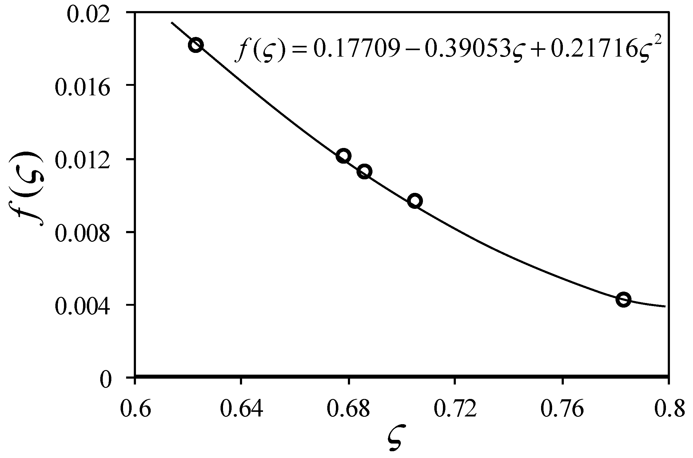
2.3. Thermal Fatigue Life Prediction Model

According to the FEM analysis and thermal fatigue tests, the failure from S45 is identified as strain-controlled creep failure [28,29]. Therefore, the basic strain-controlled fatigue law can be written as the Coffin–Manson formula:
( Δ ε ) n N f = C
where Δε is the range of strain, and n and C are the constants to be determined by experimental results.
Considering the strain range average within a characteristic failure length lε along the interfacial edge and neglecting the dependence of ς(t) on the maximum and minimum strain states, we get:
Δ ε ¯ = 1 l ε 0 l ε Δ K ε r ς d r = Δ K ε l ε ς ( 1 ς )
where Δ ε ¯ donates the average strain range within lε.
Substituting Δ ε ¯ into Equation (3), we obtain:
Δ K ε n l ε n ς ( 1 ς ) n N f = C
Here lε is always dependent on ΔKε and ς. If the separation in variables of lε is taken into account, Equation (5) can be simplified as:
( Δ K ε 1 ς ) m N f = f 1 ( ς )   or   ( Δ K ε 1 ς ) ( N f ) 1 m = f ( ς )
where f ( ς ) = f 1 1 / m ( ς ) is a function of the singular order and m is a constant.
Based on the experimental conditions outlined in this paper, the thermal fatigue life was determined, and the range of strain intensity factor was solved by numerical simulation. Figure 12 shows the relationship between Kε/(1−ς) and Nf when considering the failure from S45. The fitting lines for different chips are almost parallel to each other. This fact means that m is really a material constant, and independent to the singular orders and intensity factors. The slope equals 1/m, so m = 1/0.292. Figure 13 shows the relationship of f(ς) with singular order ς in polynomial form. Therefore, the thermal fatigue life law for S45 is finally determined as:
Δ K ε 1 ς ( N f ) 0.292 = 0.1771 0.3905 ς + 0.2172 ς 2
Theoretically, once the strain intensity factors and singular orders of new chips at the failure interface are obtained, their thermal fatigue lives can be predicted. At the same time, the calculation of thermal mechanical analysis to get the singularity parameters is not easy, and tends to be time-consuming. Therefore, the GA-BP based method discussed below needs to be established for the necessary parameters in thermal fatigue life prediction.

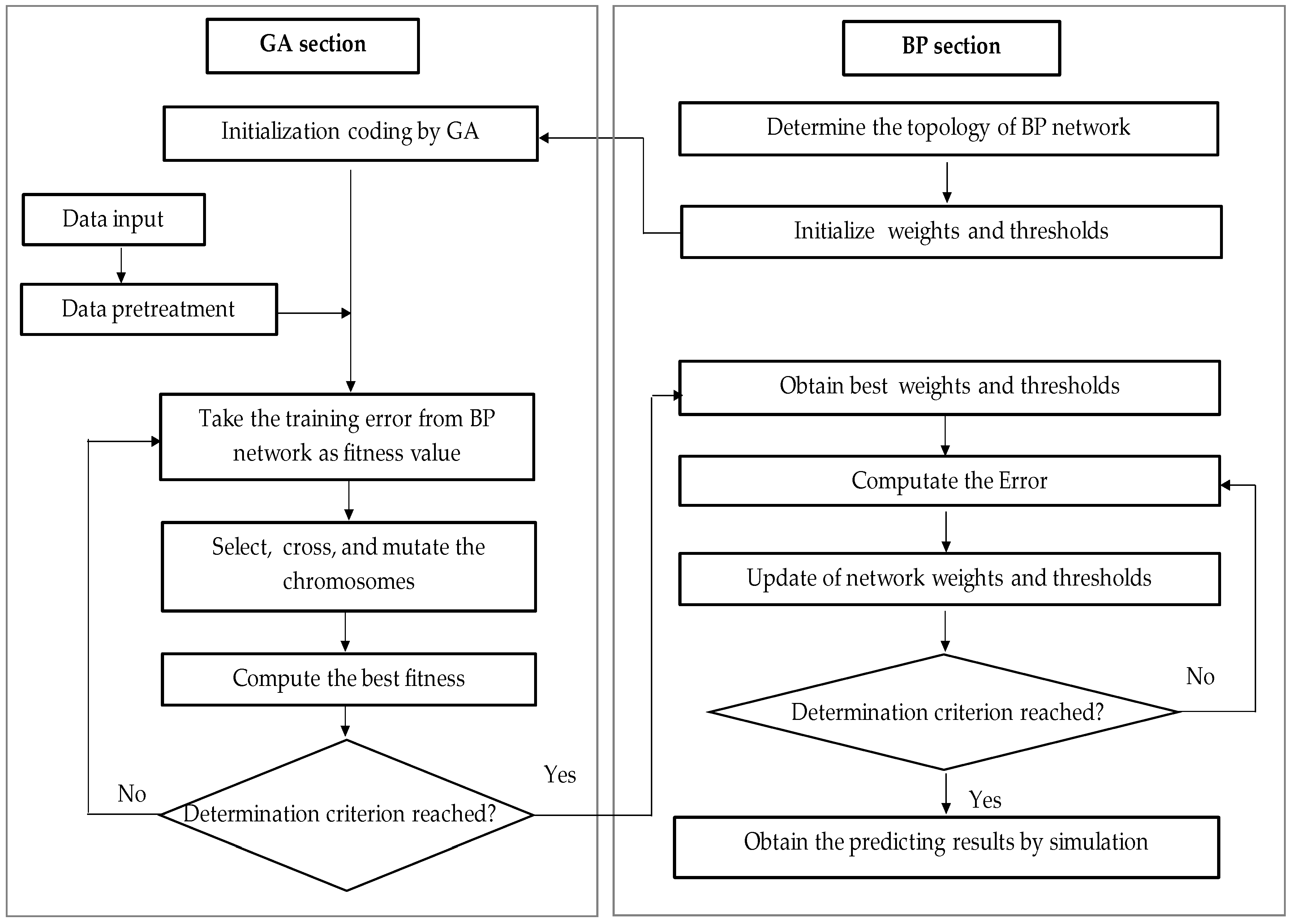
3. Method of the BP Artificial Neural Network Based on a Genetic Algorithm

3.1. GA-BP: Theoretical Background

The genetic algorithm (GA) is a domain-independent problem-solving technique, which encodes the problem into a chromosome composed of genes and generates a chromosome representing the solution to the problem through a continuous process of selecting, crossing, and mutating the chromosome. The GA operates on the chromosome code, and it isolates the characteristics of the problem itself, so it has wide adaptability. At the same time, since the algorithm operates in parallel from multiple initial points, the search process is free from convergence to a local extremum. The GA implements the search process through groups, making it different from a single-point search and easy to parallelize, thus improving the efficiency of the algorithm [30,31].
The classic back propagation (BP) is a three, or more than three, layer hierarchical forward neural network. The BP algorithm consists of two parts: the forward transmission of information and the back propagation of errors. In the forward transmission, the input information from the input layer passes to the output layer through the hidden layer. If the desired output is not obtained at the output layer, the error change of the output layer is calculated and passed back along the original connection path, to modify the weight of each layer of neurons until the desired goal is reached [32]. Mathematically, the BP model works based on an error gradient descent criterion, and its calculation process is a process of obtaining a smaller error. However, it is often unable to achieve global convergence and falls into local minima when solving complex problems, resulting in an invalid learning process. Additionally, the learning algorithm converges slowly, especially near the target. Finally, the input and output nodes of the network are determined by the specific problem to be studied, but the selection of hidden nodes is often based on experience and is short of theoretical guidance.
The GA is an effective way to avoid the above problems. To maintain a certain size of population, the GA handles several points in the search space, rather than a single point as in the gradient descent method, which helps the search for the global best and is free from the local minimum [33]. This can avoid the defect of the gradient descent method when used in a BP artificial neural network, and ensure a good convergence speed [34].

3.2. GA-BP Hybrid Programming

The main idea of GA-BP hybrid programming is to optimize the weights and thresholds of the BP network based on the GA. Real coding is used to evolve the weights and thresholds of the network. Firstly, the fitness function is determined, then the evolution process (the global search operator of the algorithm, such as the selection, crossover and mutation operator) is selected. Lastly, the GA searches for the optimal weights and thresholds in the whole solution space. The algorithm flow chart of a real coding genetic algorithm combined with a neural network is shown in Figure 14. In essence, the main role of the GA is to optimize the initial weight distribution and locate some better search spaces in the solution space, which facilitates the BP algorithm’s search for the optimal solution in these small solution spaces. Generally, the efficiency of the GA-BP hybrid training is superior to BP training alone.

4. GA-BP Model Developed for Thermal Fatigue Life Prediction

4.1. Variables in the Model

The main aim of the present investigation is to employ GA and BP programming to predict the singular orders and strain intensity factors under thermal fatigue cycles, and then calculate the thermal fatigue lives of microelectronic chips under different conditions according to the established thermal fatigue law. The singular orders and strain intensity factors at the failure interface are always dependent on the loading condition, geometry and thermal mechanical properties of the solder, and so forth, while the connections between them cannot be explicitly expressed. Therefore, it is user-friendly to clear these mathematical difficulties by a black box. The singular orders and strain intensity factors can be expressed in the following form:
K ε , ς = f ( load   condition ,   geometry ,   material   properties ,   )
It is possible to estimate the singular orders and strain intensity factors by a trained neural network instead of FEM analysis. However, to train an efficient neural network, it is necessary to have a huge amount of FEM analysis results as the samples for training. Once the neural network is well trained, the singular orders and strain intensity factors can be obtained easily. To reach the stated goal, four variables—elasticity of modulus E, thickness h and width d of solder SnAg3Cu0.5, and cyclic peak temperature Tmax—are considered as the parameters of the input layer of the GA-BP network, as shown in Figure 15. According to the different values of the input variables, 60 sets of test samples are prefabricated from the FEM simulation, from which 50 sets are selected as training data, and the remaining 10 sets are used as testing data. To achieve the efficient learning of the GA-BP programming, various parameters such as population size, number of generations, function set, mutation rate, crossover rate, and so forth need to be set in advance [35]. The optimum combination of values of the above parameters is obtained by the performance of several trials, as given in Table 3.

4.2. Predicted Results

The predicted singular strain orders and intensity factors of the steady state of S45 are listed in Table 4. The performance of the GA-BP models in the fatigue life prediction is statistically evaluated using two prediction score metrics calculated from the test dataset: the coefficient of correlation (R2) and mean-square error (MSE). The calculated R2 and MSE are 0.9578 and 1.8527, respectively. The trained neural network can predict the singular parameters with good accuracy. The thermal fatigue lives, based on the predicted singular orders and strain intensity factors, are calculated and compared with the tested ones, as depicted in Figure 16. The result shows that the difference between the predicted output and tested output is small, meeting the error requirement. Therefore, the method of GA-BP in predicting the thermal fatigue lives of microelectronic chips is feasible.

5. Conclusions

The present study outlines an efficient approach for the prediction of thermal fatigue of microelectronic chips under cyclic thermal loading, using GA-BP hybrid programming. From the result of the present investigation, it is observed that the prediction accuracy of the thermal fatigue life by the developed GA-BP method is in good agreement with the experimental results. The application of thermal fatigue life prediction demonstrates that the thermal fatigue of chips can be evaluated uniformly, no matter what the shapes, materials and loading types are, as long as the relevant stress-strain intensity factors and singular orders can be obtained.
However, as shown by the outcome of numerical analysis and experimental results, the thermal fatigue model involved several factors such as the thermal fatigue failure mode, the diversification of singular parameters in FEM analysis, and the determination and measurement of thermal fatigue life during experiments throughout the modeling process. This causes certain restrictions in its application. Further research based on other computational intelligence approaches, like computational intelligence aided design, should be employed to improve the prediction accuracy of the established thermal fatigue model.

Author Contributions

X.H. conceived and designed theory and experiments, and wrote the primary manuscript; Z.H. contributed experiments, FEM analysis and data analysis.

Acknowledgments

This research work is supported by the National Natural Science Foundation of China (No. 51404286), and the Fundamental Research Funds for the Central Universities of China (No. 17CX02065). The authors are also grateful for the financial support from China Scholarship Council (No. 201806455016).

Conflicts of Interest

The authors declare no conflict of interest.

References

  1. Lee, W.W.; Nguyen, L.T.; Selvaduray, G.S. Solder joint fatigue models: review and applicability to chip scale packages. Microelectron. Reliab. 2000, 40, 231–244. [Google Scholar] [CrossRef]
  2. Su, S.N.; Akkara, F.J.; Abueed, M.; Jian, M.H.; Hamasha, S.; Suhling, J.; Lall, P. Fatigue properties of lead-free doped solder joints. In Proceedings of the 2018 17th IEEE Intersociety Conference on Thermal and Thermomechanical Phenomena in Electronic Systems (ITherm), San Diego, CA, USA, 29 May–1 June 2018; pp. 1243–1248. [Google Scholar]
  3. Zhu, Q.S.; Gao, F.; Ma, H.C.; Liu, Z.Q.; Guo, J.D.; Zhang, L. Failure behavior of flip chip solder joint under coupling condition of thermal cycling and electrical current. J. Mater. Sci. Mater. Electron. 2018, 29, 5025–5033. [Google Scholar] [CrossRef]
  4. Xu, A.Q.; Nied, H.F. Finite element analysis of stress singularities in attached flip chip packages. ASME J. Electron. Packag. 2000, 122, 301–305. [Google Scholar] [CrossRef]
  5. Erinc, M.; Schreurs, P.J.G.; Geers, M.G.D. Integrated numerical-experimental analysis of interfacial fatigue fracture in SnAgCu solder joints. Int. J. Solids Struct. 2007, 44, 5680–5694. [Google Scholar] [CrossRef]
  6. Xiong, M.Y.; Zhang, L. Interface reaction and intermetallic compound growth behavior of Sn-Ag-Cu lead-free solder joints on different substrates in electronic packaging. J. Mater. Sci. 2019, 54, 1741–1768. [Google Scholar] [CrossRef]
  7. Vandevelde, B.; Gonzalez, M.; Limaye, P.; Ratchev, P.; Beyne, E. Thermal cycling reliability of SnAgCu and SnPb solder joints: A comparison for several IC-packages. Microelectron. Reliab. 2007, 47, 259–265. [Google Scholar] [CrossRef]
  8. Syed, A.R. Accumulated creep strain and energy density based thermal fatigue life prediction models for SnAgCu solder joints. In Proceedings of the 54th Electronic Components and Technology Conference (IEEE Cat. No.04CH37546), Las Vegas, NV, USA, 4 June 2004; pp. 737–746. [Google Scholar]
  9. Pang, J.H.L.; Tan, T.I.; Sitaraman, S.K. Thermo-mechanical analysis of solder joint fatigue and creep in a flip chip on board package subjected to temperature cycling loading. In Proceedings of the 48th IEEE Electronic Components and Technology Conference, Seattle, WA, USA, 25–28 May 1998; pp. 878–883. [Google Scholar]
  10. Zhu, S.P.; Huang, H.Z.; He, L.P.; Liu, Y.; Wang, Z.L. A generalized energy-based fatigue-creep damage parameters for life prediction of turbine disk alloys. Eng. Fract. Mech. 2012, 90, 89–100. [Google Scholar] [CrossRef]
  11. Hattori, T.; Sakata, S.; Murakami, G. A stress singularity parameter approach for evaluating the interfacial reliability of plastic encapsulated lsi devices. ASME J. Electron. Packag. 1989, 111, 243–248. [Google Scholar] [CrossRef]
  12. Gradin, P.A. A fracture criterion for edge-bonded bimaterial bodies. J. Compos. Mater. 1982, 16, 448–456. [Google Scholar] [CrossRef]
  13. Groth, H.L. Stress singularities and fracture at interface corners in bonded joints. Int. J. Adhes. Adhes. 1988, 8, 107–113. [Google Scholar] [CrossRef]
  14. Reedy, E.D., Jr.; Guess, T.R. Comparison of butt tensile strength data with interface corner stress intensity factor prediction. Int. J. Solids Struct. 2007, 30, 2929–2936. [Google Scholar] [CrossRef]
  15. Liang, J.; Gollhardt, N.; Lee, P.S.; Heinrich, S.; Schroeder, S. An integrated fatigue life prediction methodology for optimum design and reliability assessment of solder interconnections. In Proceedings of the Pacific Rim/ASME International Intersociety Electronic and Photonic Packaging Conference, Kohala Coast, HI, USA, 15–19 June 1997; pp. 1583–1592. [Google Scholar]
  16. Kim, D.G.; Kim, J.W.; Jung, S.B. Evaluation of solder joint reliability in flip chip package under thermal shock test. Thin Solid Films 2006, 504, 426–430. [Google Scholar] [CrossRef]
  17. Munz, D.; Yang, Y.Y. Stress singularities at interface in bonded dissimilar materials under mechanical and thermal loading. J. Appl. Mech. 1992, 59, 857–861. [Google Scholar] [CrossRef]
  18. Liu, S.Q.; McDonald, S.; Sweatman, K.; Nogita, K. The effects of precipitation strengthening and solid solution strengthening on strain rate sensitivity of lead-free solders: Review. Microelectron. Reliab. 2018, 84, 170–180. [Google Scholar] [CrossRef]
  19. Pleune, T.T.; Chopra, O.K. Using artificial neural networks to predict the fatigue life of carbon and low-alloy steels. Nucl. Eng. Des. 2000, 197, 1–12. [Google Scholar] [CrossRef]
  20. Venkatesh, V.H.; Rack, J. A neural network approach to elevated temperature creep-fatigue life prediction. Int. J. Fatigue 1999, 21, 225–234. [Google Scholar] [CrossRef]
  21. Haque, M.E.; Sudhakar, K.V. Prediction of corrosion-fatigue behavior DP steel through artificial neural network. Int. J. Fatigue 2001, 23, 1–4. [Google Scholar] [CrossRef]
  22. Kropat, E.; Weber, G.W. Fuzzy target-environment networks and fuzzy-regression approaches. Am. Inst. Math. Sci. 2018, 8, 135–155. [Google Scholar] [CrossRef]
  23. Mohantya, J.R.; Mahantaa, T.K.; Mohantyb, A.; Thatoi, D.N. Prediction of constant amplitude fatigue crack growth life of 2024 T3Al alloy with R-ratio effect by GP. Appl. Soft Comput. 2015, 26, 428–434. [Google Scholar] [CrossRef]
  24. Ding, S.F.; Su, C.Y.; Yu, J.Z. An optimizing BP neural network algorithm based on genetic algorithm. Artif. Intell. Rev. 2011, 36, 153–162. [Google Scholar] [CrossRef]
  25. Conkey, D.B.; Brown, A.N.; Caravaca-Aguirre, A.M.; Piestun, R. Genetic algorithm optimization for focusing through turbid media in noisy environments. Opt. Express 2012, 20, 4840–4849. [Google Scholar] [CrossRef] [PubMed]
  26. Vassilopoulos, A.P.; Bedi, R. Adaptive neuro-fuzzy inference system in modelling fatigue life of multidirectional composite laminates. Comput. Mate. Sci. 2008, 43, 1086–1093. [Google Scholar] [CrossRef]
  27. Huang, X.G.; Han, Z.Y. Interface singular field analysis and thermal fatigue failure of solder joint in a stacked electronic modules. J. Mater. Sci. Mater. Electron. 2016, 27, 8299–8311. [Google Scholar] [CrossRef]
  28. Qian, Z.F.; Lu, M.F.; Ren, W.; Liu, S. Fatigue life prediction of flip-chips in terms of nonlinear behaviors of solder and underfill. In Proceedings of the 49th Electronic Components and Technology Conference (Cat. No.99CH36299), San Diego, CA, USA, 1–4 June 1999; pp. 141–148. [Google Scholar]
  29. Chen, X.; Song, J.; Kim, K.S. Fatigue life of 63Sn–37Pb solder related to load drop under uniaxial and torsional loading. Int. J. Fatigue 2006, 28, 767–776. [Google Scholar] [CrossRef]
  30. Whitley, D. A genetic algorithm tutorial. Stat. Comput. 1994, 4, 65–85. [Google Scholar] [CrossRef]
  31. Leung, Y.W.; Wang, Y.P. An orthogonal genetic algorithm with quantization for global numerical optimization. IEEE Trans. Evol. Comput. 2001, 5, 41–53. [Google Scholar] [CrossRef]
  32. Yao, X.; Liu, Y. A new evolutionary system for evolving artificial neural networks. IEEE Trans. Neural Netw. 1997, 8, 694–713. [Google Scholar] [CrossRef]
  33. Cook, D.F.; Ragsdale, C.T.; Major, R.L. Combining a neural network with a genetic algorithm for process parameter optimization. Eng. Appl. Artif. Intell. 2000, 13, 391–396. [Google Scholar] [CrossRef]
  34. Gupta, J.N.D.; Sexton, R.S. Comparing backpropagation with a genetic algorithm for neural network training. Omega 1999, 27, 679–684. [Google Scholar] [CrossRef]
  35. Genel, K. Application of artificial neural network for predicting strain-life fatigue properties of steels on the basis of tensile tests. Int. J. Fatigue 2004, 26, 1027–1035. [Google Scholar] [CrossRef]
Figure 1. Power chipset.
Electronics 08 00542 g001
Figure 2. Structure of a single chip.
Electronics 08 00542 g002
Figure 3. Temperature cycle for thermal fatigue tests.
Electronics 08 00542 g003
Figure 4. RI of chip Q2 vs. thermal cycles.
Electronics 08 00542 g004
Figure 5. SEM observation of crack nucleation of chip Q2 at S12 and S45.
Electronics 08 00542 g005
Figure 6. FEM model of chip Q2.
Electronics 08 00542 g006
Figure 7. Specific points A and B at the interfacial edges.
Electronics 08 00542 g007
Figure 8. Stress distribution at points A and B.
Electronics 08 00542 g008
Figure 9. Strain distribution at points A and B.
Electronics 08 00542 g009
Figure 10. Stress singularity at maximum stress state.
Electronics 08 00542 g010
Figure 11. Strain singularity at maximum strain state.
Electronics 08 00542 g011
Figure 12. Relationship between Δ K ε / ( 1 ς ) and N f .
Electronics 08 00542 g012
Figure 13. Determination of f ( ς ) .
Electronics 08 00542 g013
Figure 14. Flow chart of a GA-BP neural network.
Electronics 08 00542 g014
Figure 15. Architecture of the BP artificial neural network.
Electronics 08 00542 g015
Figure 16. Error band scatter of the predicted thermal fatigue lives with the GA-BP method.
Electronics 08 00542 g016
Table 1. Thermal cyclic fatigue test results.
Chip TypeQ1Q2Q3Q4Q5
Nf (Tmax = 150 °C)650750690550615
Nf (Tmax = 120 °C)14001500143012201310
Nf (Tmax = 100 °C)24303150298025402330
Table 2. Analysis results of maximum strain fields.
Chip TypeInterface EdgeMaximum Strain State
ςKς (mmς)
Q1S120.622 0.000447
S450.532 0.001150
Q2S120.789 0.000151
S450.687 0.000238
Q3S120.762 0.000138
S450.705 0.000176
Q4S120.745 0.000157
S450.678 0.000163
Q5S120.658 0.000221
S450.784 0.000067
Table 3. Parameters of the GA-BP model.
ParameterImplicationRange
P1Population size1000
P2Function setpower
P3Number of generation100–5000
P4Probability of reproduction0.1
P5Probability of crossover0.9
P6Maximum depth of initial random organisms4
P7Maximum depth of organisms after crossover10
Table 4. Predicted singular parameters at the maximum strain state.
Sample
No.
Chip Typeh
/mm
d
/mm
E
/GPa
Tmax
/°C
Predicted
ς
Estimated
ς
Error
/%
Predicted
Kς
Estimated
Kς
Error
/%
1I0.24 6.642.10 1500.8310.8512.350.0009740.0010507.24
2I0.22 7.041.621200.5840.6226.110.0008210.0008553.98
3II0.22 6.640.95 1500.6550.6874.660.0004780.0004984.02
4II0.22 6.840.63 1200.6930.687−0.870.0003980.0004256.35
5III0.23 6.439.81 1500.7510.705−6.520.0004120.0004253.06
6III0.21 6.643.58 1200.7460.705−5.820.0003240.0003425.26
7IV0.24 6.642.15 1500.6470.6784.570.0004840.0005237.46
8IV0.22 7.044.17 1200.6910.678−1.920.0004190.0004455.84
9V0.21 6.638.95 1500.7370.7845.990.0001580.000149−6.04
10V0.22 6.843.61 1200.7520.7844.080.0001210.000115−5.22

