Article

Compact Printable Inverted-M Shaped Chipless RFID Tag Using Dual-Polarized Excitation

by
Wazie M. Abdulkawi
1,*,
Abdel-Fattah A. Sheta
1,
Khaled Issa
2 and
Saleh A. Alshebeili
1,2
1
Department of Electrical Engineering, King Saud University, Riyadh 11421, Saudi Arabia
2
KACST-TIC in Radio Frequency and Photonics for the e-Society (RFTONICS), Electrical Engineering Department, King Saud University, Riyadh 11421, Saudi Arabia
*
Author to whom correspondence should be addressed.
Electronics 2019, 8(5), 580; https://doi.org/10.3390/electronics8050580
Submission received: 24 April 2019 / Revised: 18 May 2019 / Accepted: 22 May 2019 / Published: 25 May 2019
(This article belongs to the Special Issue Advanced RFID Technology and Applications)

Abstract

:
A novel and compact dual-polarized (DP) chipless radio-frequency identification (RFID) tag is presented in this paper. This tag can read both vertical and horizontal orientations within its frequency band, which improves the robustness and detection capability of the RFID system. The proposed tag makes use of the slot length variation encoding technique to improve the encoding capacity. This technique can duplicate the encoding capacity, thereby reducing the overall tag size by almost 50%. In particular, the proposed tag has an encoding capacity of 20 bits in the 3–8 GHz frequency band and achieves data density of around 15.15 bits/cm2. Three prototypes are fabricated and tested outside an anechoic chamber. Furthermore, one tag is tested at different distances (10 cm, 30 cm, and 60 cm) from the reader and the measured results are compared. The simulated and measured results are in reasonable agreement, with acceptable shifts at some frequencies due to fabrication and experimental errors.

1. Introduction

Radio frequency identification technology (RFID) is a wireless system that uses radio frequency electromagnetic fields to exchange data between tags attached to an object and a reader device, which sends interrogator signals for identification. The conventional RFID tag contains an integrated circuit (IC), which is a main source of the increase in its cost. A new RFID structure has been investigated in the last few years. This new structure does not contain a silicon chip and it is called chipless RFID. Different methods have been reported in recent years for data encoding in chipless RFID tags. Generally, these encoding methods can be classified in various domains, as in time, frequency, and phase. In addition, hybrid-domain encoding techniques can improve the tag code detection [1]. In time domain (TD) based tags, the RFID reader interrogates the tag with a sequence of pulses. Then, the tag code can be estimated from the echoes reflected from a set of reflectors implemented on the tag attached to an object. In other words, existence or absence of these echoes and their time positions are used to identify the tag code [2,3]. In frequency domain (FD) based tags, the RFID reader interrogates the tag with an RF signal and then the tag retransmits the frequency signature to the reader. Each data bit represents the presence or absence of a resonant frequency in the operating spectrum [4,5,6,7]. Phase domain (PD) based encoding technique was presented in [8]. In that work, three square microstrip patch antennas loaded with three open circuit stubs are suggested to encode three bits. Varying the length of the stub alters the phase of the backscattered signal. In the hybrid domain (HD) encoding techniques, more than one domain is used [9,10]. However, as mentioned in [3], for significant numbers of bits, HD techniques still require very high spectral bandwidth and the resultant configuration, in this case, will not be matched for low-cost readers.
Back to frequency domain, chipless RFID tags can be operated either in retransmission-mode or in backscattered-mode. Retransmission based chipless RFID tags use multi-resonator circuits and two UWB antennas for data transmission and reception [11,12]. The retransmission-based tags suffer due to their large size and complex structure [13].
In contrast to retransmission-mode, backscattering based tags consists only of resonating elements (scatterers) where no separate antennas are required [14,15,16]. Therefore, significant area reduction can be achieved. In addition to area saving, increasing data density is still a real challenge in the chipless RFID systems. In literature, the number of chipless RFID tags is proposed to enhance the data capacity and the detection methods. For example, slot length variation can be exploited in order to double the data capacity in the same frequency band [6]. In [17,18], Multiple I- and U-slots dual polarized resonators etched on a rectangular patch are proposed in the frequency range 6–13 GHz. The slot resonators (I or U) are reused in both vertical and horizontal polarizations. Recently, some dual polarized structures have been investigated, such as the L-shaped strips [19] and square loop [20]. Polarization insensitive structures, such as the triangular loops [21], circular loops [22], and multiple L-strips resonators [23], have also been studied. The advantage of these structures is that the tag data can be read from any orientation by the reader antennas.
This paper presents a 20 bits compact very high density chipless RFID tag by using inverted M-shaped multiple slots resonators. This compact tag uses the dual polarized technique to improve the detection method, and slot length variation to double the encoding capacity in the same frequency band. A tag of 20 bits encoding capacity is designed and analyzed. The proposed tag is simulated using a computer simulation technology (CST) EM simulator as an infinite structure. This paper is organized as follows: Section 2 presents the proposed chipless RFID tag. Section 3 presents the simulation results of some Inverted-M chipless RFID tags. In Section 5, three prototypes of the proposed tag are experimentally validated. Finally, concluding remarks are given in Section 6.

2. Proposed Chipless RFID Tag

Figure 1 shows the proposed DP chipless RFID tag. This tag consists of a conductive rectangular patch overloaded with sets of inverted M slots. The resonance frequency of a half wave slot resonator can be calculated approximately using the expression [24]:
f = c 2 l 2 1 + ε r
where l is the total physical slot length of the M-shaped resonator, c is the speed of light, and ε r is the permittivity of the substrate. In this paper, the tag is designed using Rogers RT5880 substrate having thickness (h = 0.256 mm) and permittivity ( ε r = 2.2).
As shown in Figure 1, l and w are the length and width of the rectangular patch. sx is the separation distance between the vertical slots, while sy is approximately defined as the separation distance between the slanted slots, and ws is the width of all slots. Each slot resonator can be positioned in either the active or the passive mode of operation. A diagram of ten slot resonators in the active mode is presented in Figure 2a. The slot resonators can be made inactive by adding five short circuits at different parts of the resonator, as shown in Figure 2b.
The main physical dimensions of the tag shown in Figure 1 are listed in Table 1. All slot resonators have the same separation distances between the vertical slots (sx) and different separation distances between the slanted slots (sy) as indicated in Table 2.
The length of each slot resonator is determined by the following formula (i = 1, 2, …, 9, 10):
l i = c 2 f i 2 1 + ε r
li represents the total length of the ith slot resonator and can be written according to the notation in Figure 1 as:
l i = 2 ( l i + l i ) ( i = 1 ,   2 ,   ,   7 ,   8 ) ,
l 9 = 2 ( l 9 + l 9 + l 9 ) ,
l 10 = 2 ( l 10 + l 10 + l 10 + l 10 ) .
The designed tag is optimized to produce deep notches at the desired frequencies in the operating frequency range from 3 GHz to 8 GHz. Initially, one novel inverted-M-shaped slot resonator is designed to obtain one notch in the desired frequency range. Afterwards, by optimization, inverted-M resonators are added to obtain multiple notches in the mentioned frequency range. By this process, the number of notches can be controlled by adding or removing the inverted-M slot resonators. In our case, ten optimized inverted-M slots were utilized to obtain ten notches. To ensure the compactness of the structure, the available area was utilized efficiently by twisting the last two slot resonators. The length of the slot resonator decreases as the value of the resonance frequency increases. The resonance frequencies can be calculated using Equation (1), depending on the physical dimensions of each slot.
Slot number 1 gives the lowest resonant frequency because of its longest length and as it corresponds to the most significant bit (MSB). By contrast, the least significant bit (LSB) is related to the smallest slot length (slot number 10) that resonates at maximum frequency. The reflection coefficients are computed when the tag is excited with vertically and horizontally polarized waves. These waves are incident normal to the chipless RFID tag surface. When the plane wave excites the tag, a much higher surface current is induced around the slots at its resonant frequency. These orthogonal polarities are utilized to double the encoding capacity [25,26].
Therefore, the proposed structure shows a frequency-selective behavior with deep notches at all resonant frequencies. These notches (resonance frequencies) can be controlled by adding short circuits in each slot. In the developed tag, ten bits are achieved using ten vertically polarized slots and another ten bits are accomplished from the ten horizontally polarized slots on the conductive rectangular patch. Logically, the active slot resonator represents logic 1 and the passive resonator represents logic 0. Therefore, the designed tag in Figure 2a denotes logic (1111111111) and the tag in Figure 2b indicates logic (0000000000).

3. Simulation Results

The proposed tag is designed and simulated using CST Microwave Studio. Backscattered chipless RFID tags can be analyzed either using monostatic or bistatic reader system. Bistatic systems use two antennas—one for transmitting and one for receiving. However, monostatic systems use a single antenna for both interrogating and reading purposes, and therefore they are usually less expensive than bistatic systems.
The simulation setup of the DP chipless RFID tag is shown in Figure 3. The tag can be excited by either a vertically or horizontally polarized plane wave. In each case, the backscatter field is received and the frequency signature of the tag can be identified from the reflection coefficient response S11.
To validate the concept, four different passive tags are designed and simulated. The proposed tag with four different bit configurations 1111111111, 0000000000, 0101010101, and 1010101010 is shown in Figure 2a,b and Figure 4a,b, respectively.
Figure 5 shows the reflection coefficients S11 of the designed chipless RFID tag structures that have all ones (1111111111) and all zeros (0000000000) for both vertically and horizontally plane waves. Table 3 illustrates the total length and the corresponding frequency of each slot resonator (using Equation (1)). Twenty resonances are observed in the backscattered signal from the designed tag of the all-ones state. Ten frequency signatures are related to the vertically polarized wave and ten signatures from the horizontally polarized wave. These resonance frequencies are listed in Table 3, where we observe that the maximum difference between the resonance frequencies for both polarizations is approximately 104 MHz and the minimum difference is approximately 8 MHz.
On the other hand, Figure 6 and Figure 7 show the frequency responses of two other tags with alternating ones and zeros: (1010101010) and (0101010101), respectively. These responses are achieved under vertical and horizontal plane-wave excitations. The shift in frequency between the two responses is necessary to achieve a very sharp peak-to-peak difference between the two curves [14]. Figure 8 shows the difference in dBs between the vertical and horizontal polarized S11 of Figure 5 (code: 1111111111). Additionally, the difference between the vertical and horizontal polarized S11 for the codes 1010101010 and 0101010101 is reported in Figure 9 and Figure 10, respectively. Sharp peak-to-peak response is observed for all-ones codes.

4. The 20-Bit Dual Polarized Tag

The resonance frequency of the slotted line is inversely proportional to the slot length. Thus, increase in the slot length will decrease its resonance frequency and vice versa. Therefore, each resonator can be represented by one of the four possible states: 00, 10, 01, and 11. The first state, 00, is obtained when the resonator is short-circuited. No resonance can be observed in the band of operation. The second state (11) is related to resonator’s length li and subsequently resonance frequency fi. In the third case (10), the length of the slot “i” is slightly increased. This slight modification results in a shift in the resonance frequency from fi to fi. A slight decrease in slot “i” length will result in a shift in the resonance frequency from fi to fi. This is the fourth state (01). Therefore, the encoding capacity (bits) and encoding density (bits/cm2) will be doubled within the fixed frequency band. Table 4 illustrates the all-possible states. The simulated S11 for these cases are illustrated in Figure 11 for all 10 active resonators. Table 5 figures out the corresponding frequencies for the proposed tag with increasing and decreasing slot lengths. As listed in Table 5, the maximum difference between the resonance frequencies for both variations is approximately 280 MHz and the minimum difference is approximately 40 MHz.

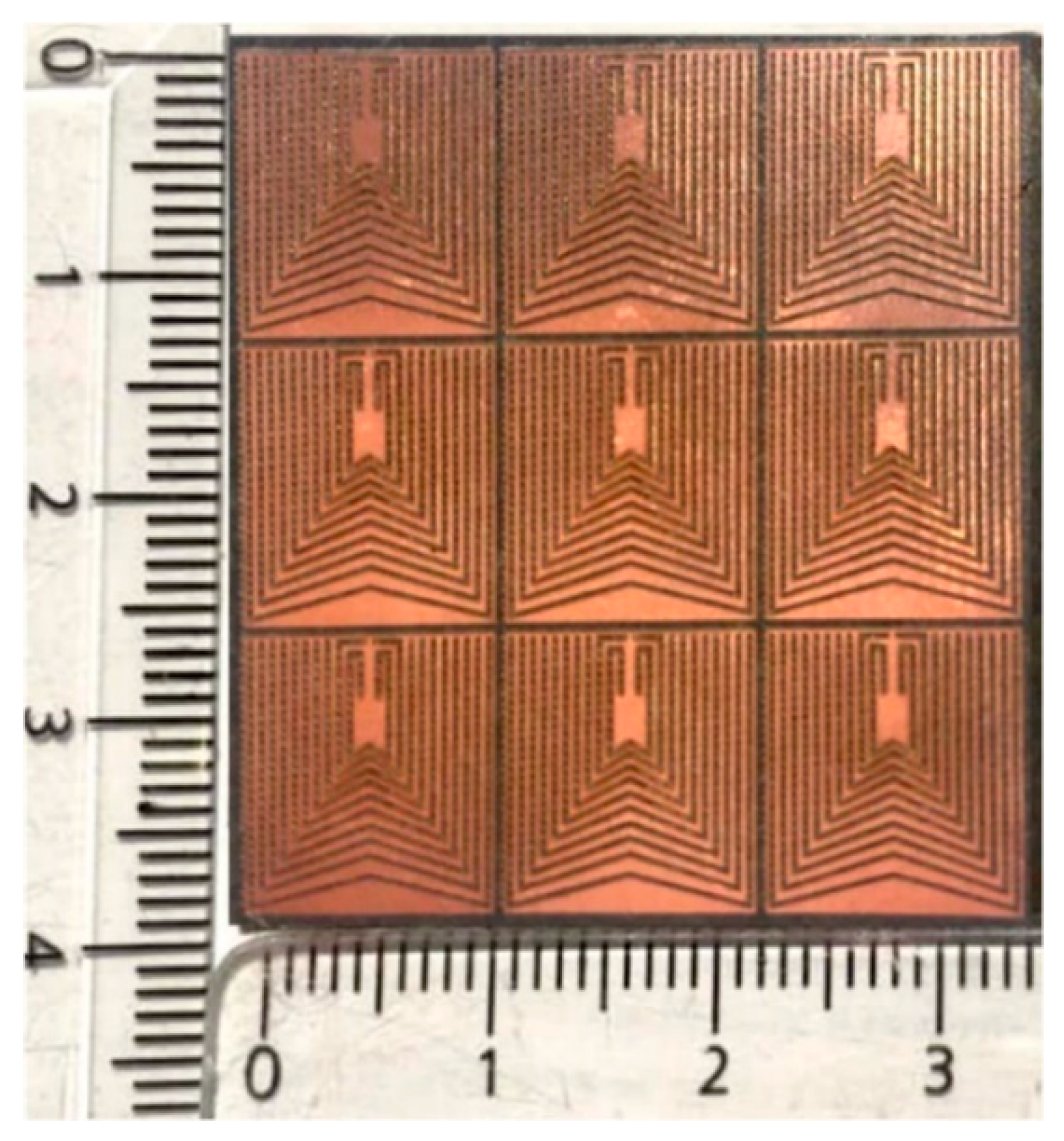
5. Experimental Validation

In order to validate the proposed concept, three prototypes were fabricated and measured in a normal environment. The ID codes of these prototypes are 11111111111111111111, 11001100110011001100, and 00110011001100110011. The simulated reflection coefficients were the results of an infinite array of the proposed tag. However, the manufactured tags were reduced to a finite 3 × 3 array of unit cells in order to decrease the physical size as much as possible. The physical dimensions of the 3 × 3 array of unit cells were 37.6 × 34.6 mm2, as illustrated in Figure 12. The three fabricated tags, shown in Figure 12 and Figure 13, were measured in both vertically and horizontally polarized orientations using the measurement setup depicted in Figure 14. The frequency responses of the fabricated tags were measured using the two-port PNA-X microwave network analyzer (N5242A) and a broadband horn antenna operating from 1 to 18 GHz.
The measurements are performed in a normal environment (outside an anechoic chamber). In this case, the back scattered signal received by the reader (horn antenna connected to the network analyzer) consists of the reflected signal from the horn antenna impedance mismatch, the required frequency signature signal from the tag, the reflected signal from the metallic structure of the tag, the clutter noise from the surroundings, and the white noise. The effect of the horn impedance mismatch and the clutter noise can be approximately removed by an appropriate calibration technique [23,27,28]. In this work, the calibration method is employed by subtracting the reflection coefficient (S11) of the measurement system without a tag from the reflection coefficient (S11) with a tag.
The simulated and measured results for the fabricated prototypes are compared in Figure 15 (horizontal orientation) and Figure 16 (vertical orientation). The tag was positioned at a distance of 10 cm from the horn antenna (chipless RFID reader). Figure 15a shows the presence of ten nulls (code: 11111111111111111111) for horizontal polarization over the desired frequency band. The measured results are in reasonable agreement with the simulated ones, with slight shifts at some frequencies. This frequency shift may be attributed to material parameters variations and fabrication accuracy. Therefore, the frequency shifts of a given slot in the various states (01, 10, and 11) occur approximately in the same way. In this case, calibration using some samples (prototypes) could be used in practical applications to reduce errors due to any frequency shift.
For further validation, the all-ones tag was tested for different distances (10 cm, 30 cm, and 60 cm). The measured results are compared in Figure 17. The effectiveness and accuracy of the tag can be seen from Figure 17, as the tag is distinguishable even up to a distance of 60 cm. A comparison of the designed tag with some of the existing chipless RFID tags is reported in Table 6. According to our knowledge and the comparison in Table 6, the proposed tag is the best in terms of coding density (bits/(GHz·cm2)) and number of bits in backscatter technique.

6. Conclusions

A novel and compact inverted-M chipless RFID tag was presented in this paper. The coding capacity was duplicated in the fixed operating bandwidth of 3 GHz to 8 GHz for the same tag size and the coding density was approximately 15.15 bits/cm2. Three prototypes were fabricated and tested outside the anechoic chamber environment with a fixed distance of 10 cm between the RFID reader and the tag being tested. Furthermore, an all-ones tag was tested at different distances from the reader (10 cm, 30 cm, and 60 cm) and the measured results were compared. The simulated and measured results were in reasonable agreement, with an acceptable shift at some frequencies due to fabrication and experimental errors. The tag response was recognized even at a distance of 60 cm.

Author Contributions

Conceptualization, K.I. and W.M.A.; methodology, W.M.A., A.-F.A.S., K.I., and S.A.A.; software, W.M.A. and K.I.; validation, W.M.A. and K.I.; formal analysis, W.M.A. and A.-F.A.S.; investigation, A.-F.A.S. and S.A.A.; resources, A.-F.A.S. and S.A.A.; data curation, W.M.A. and K.I.; writing—original draft preparation, W.M.A.; writing—review and editing, W.M.A., A.-F.A.S. and S.A.A.; visualization, W.M.A. and K.I.; supervision, A.-F.A.S. and S.A.A.

Funding

This research received no external funding.

Acknowledgments

The authors would like to thank Deanship of scientific research for funding and supporting this research through the initiative of DSR Graduate Students Research Support (GSR).

Conflicts of Interest

The authors declare no conflicts of interest.

References

  1. Preradovic, S.; Karmakar, N.C. Multiresonator-Based Chipless RFID: Barcode of the Future; Springer Science & Business Media: New York, NY, USA, 2012. [Google Scholar]
  2. Pöpperl, M.; Parr, A.; Mandel, C.; Jakoby, R.; Vossiek, M. Potential and practical limits of time-domain reflectometry chipless RFID. IEEE Trans. Microw. Theory Tech. 2016, 64, 2968–2976. [Google Scholar] [CrossRef]
  3. Herrojo, C.; Mata-Contreras, J.; Paredes, F.; Núñez, A.; Ramon, E.; Martín, F. Near-Field Chipless-RFID System With Erasable/Programmable 40-bit Tags Inkjet Printed on Paper Substrates. IEEE Microw. Wirel. Compon. Lett. 2018, 28, 272–274. [Google Scholar] [CrossRef]
  4. Islam, M.A.; Karmakar, N. A compact printable dual-polarized chipless RFID tag using slot length variation in ‘I’ slot resonators. In Proceedings of the IEEE European Microwave Conference (EuMC), Paris, France, 7–10 September 2015. [Google Scholar]
  5. Adbulkawi, W.M.; Sheta, A.A. A Compact Chipless RFID Tag Based on Frequency Signature. In Proceedings of the 9th IEEE-GCC Conference and Exhibition (GCCCE), Manamah, Bahrain, 8–11 May 2011. [Google Scholar]
  6. Islam, M.A.; Karmakar, N.C. Real-World Implementation Challenges of a Novel Dual-Polarized Compact Printable Chipless RFID Tag. IEEE Trans. Microw. Theory Tech. 2015, 63, 4581–4591. [Google Scholar] [CrossRef]
  7. Adbulkawi, W.M.; Sheta, A.-F.A. Printable Chipless RFID Tags for IoT Applications. In Proceedings of the 1st International Conference on Computer Applications & Information Security (ICCAIS), Riyadh, Saudi Arabia, 4–6 April 2018. [Google Scholar]
  8. Balbin, I.; Karmakar, N.C. Phase-Encoded Chipless RFID Transponder for Large-Scale Low-Cost Applications. IEEE Microw. Wirel. Compon. Lett. 2009, 19, 509–511. [Google Scholar] [CrossRef]
  9. Babaeian, F.; Karmakar, N.C. Hybrid Chipless RFID Tags—A Pathway to EPC Global Standard. IEEE Access 2018, 6, 67415–67426. [Google Scholar] [CrossRef]
  10. Vena, A.; Perret, E.; Tedjini, S. Chipless RFID tag using hybrid coding technique. IEEE Trans. Microw. Theory Tech. 2011, 59, 3356–3364. [Google Scholar] [CrossRef]
  11. Preradovic, S.; Karmakar, N.C. Chipless RFID: Barcode of the future. IEEE Microw. Mag. 2010, 7, 87–97. [Google Scholar] [CrossRef]
  12. Abdulkawi, W.M.; Sheta, A.F.A. Multi-Resonator Structure for Small Size Chipless Radio Frequency Identification Tag. Int. J. Comput. Digit. Syst. 2018, 7, 43–49. [Google Scholar] [CrossRef]
  13. Bhuiyan, M.S.; Karmakar, N.C. An efficient coplanar retransmission type chipless RFID tag based on dual-band McSrr. Prog. Electromagn. Res. 2014, 54, 133–141. [Google Scholar] [CrossRef]
  14. Costa, F.; Genovesi, S.; Monorchio, A. Normalization-Free Chipless RFIDs by Using Dual-Polarized Interrogation. IEEE Trans. Microw. Theory Tech. 2016, 64, 310–318. [Google Scholar] [CrossRef]
  15. Marindra, A.M.J.; Tian, G.Y. Chipless RFID Sensor Tag for Metal Crack Detection and Characterization. IEEE Trans. Microw. Theory Tech. 2018, 66, 2452–2462. [Google Scholar] [CrossRef]
  16. Bibile, M.A.; Karmakar, N.C. Moving Chipless RFID Tag Detection Using Adaptive Wavelet-Based Detection Algorithm. IEEE Trans. Antennas Propag. 2018, 66, 2752–2760. [Google Scholar] [CrossRef]
  17. Islam, M.A.; Karmakar, N.C. Compact Printable Chipless RFID Systems. IEEE Trans. Microw. Theory Tech. 2015, 63, 3785–3793. [Google Scholar] [CrossRef]
  18. Islam, M.A.; Karmakar, N.C. A novel compact printable dual-polarized chipless RFID system. IEEE Trans. Microw. Theory Tech. 2012, 60, 2142–2151. [Google Scholar] [CrossRef]
  19. Issa, K.; Ashraf, M.A.; AlShareef, M.R.; Behairy, H.; Alshebeili, S.; Fathallah, H. A Novel L-Shape Ultra Wideband Chipless Radio-Frequency Identification Tag. Int. J. Antennas Propag. 2017, 2017, 2823565. [Google Scholar] [CrossRef]
  20. Huang, H.-F.; Su, L. A compact dual-polarized chipless RFID tag by using nested concentric square loops. IEEE Antennas Wirel. Propag. Lett. 2017, 16, 1036–1039. [Google Scholar] [CrossRef]
  21. Islam, M.A.; Yap, Y.; Karmakar, N. ‘Δ’ slotted compact printable orientation insensitive chipless RFID tag for long range applications. In Proceedings of the 2016 9th International Conference on Electrical and Computer Engineering (ICECE), Dhaka, Bangladesh, 20–22 December 2016. [Google Scholar]
  22. Vena, A.; Perret, E.; Tedjini, S. High-capacity chipless RFID tag insensitive to the polarization. IEEE Trans. Antennas Propag. 2012, 60, 4509–4515. [Google Scholar] [CrossRef]
  23. Laila, D.; Thomas, R.; Nijas, C.M.; Mohanan, P. A novel polarization independent chipless RFID tag using multiple resonators. Prog. Electromagn. Res. 2015, 55, 61–66. [Google Scholar] [CrossRef]
  24. Dissanayake, T.; Esselle, K.P. Prediction of the Notch Frequency of Slot Loaded Printed UWB Antennas. IEEE Trans. Antennas Propag. 2007, 55, 3320–3325. [Google Scholar] [CrossRef]
  25. Islam, M.A.; Karmakar, N. Design of a 16-bit ultra-low cost fully printable slot-loaded dual-polarized chipless RFID tag. In Proceedings of the Asia-Pacific Microwave Conference 2011, Melbourne, VIC, USA, 5–8 December 2011. [Google Scholar]
  26. Khan, M.M.; Tahir, F.A.; Cheema, H.M. High capacity polarization sensitive chipless RFID tag. In Proceedings of the 2015 IEEE International Symposium on Antennas and Propagation & USNC/URSI National Radio Science Meeting, Ancouver, BC, Canada, 19–24 July 2015. [Google Scholar]
  27. Nijas, C.M.; Deepak, U.; Vinesh, P.V.; Sujith, R.; Mridula, S.; Vasudevan, K.; Mohanan, P. Low-cost multiple-bit encoded chipless RFID tag using stepped impedance resonator. IEEE Trans. Antennas Propag. 2014, 62, 4762–4770. [Google Scholar] [CrossRef]
  28. Sajitha, V.R.; Nijas, C.M.; Roshna, T.K.; Vasudevan, K.; Mohanan, P. Compact cross loop resonator based chipless RFID tag with polarization insensitivity. Microw. Opt. Technol. Lett. 2016, 58, 944–947. [Google Scholar] [CrossRef]
  29. Costa, F.; Genovesi, S.; Monorchio, A. A chipless RFID based on multiresonant high-impedance surfaces. IEEE Trans. Microw. Theory Tech. 2013, 61, 146–153. [Google Scholar] [CrossRef]
  30. Rance, O.; Siragusa, R.; Lemaitre-Auger, P.; Perret, E. Toward RCS magnitude level coding for chipless RFID. IEEE Trans. Microw. Theory Tech. 2016, 64, 2315–2325. [Google Scholar] [CrossRef]
  31. Svanda, M.; Polivka, M.; Havlicek, J.; Machac, J. Chipless RFID tag with an improved magnitude and robustness of RCS response. Microw. Opt. Technol. Lett. 2017, 59, 488–492. [Google Scholar] [CrossRef]
Figure 1. Geometry of the tag.
Electronics 08 00580 g001
Figure 2. Ten inverted-M chipless RFID tags (a) active mode and (b) passive mode.
Electronics 08 00580 g002
Figure 3. Simulation setup for the proposed tag.
Electronics 08 00580 g003
Figure 4. Designed tag with two different bit combinations: (a) “0101010101” and (b) “1010101010”.
Electronics 08 00580 g004
Figure 5. Amplitude reflection coefficients of the vertical (VP) and horizontal (HP) polarizations for states “1111111111” and “0000000000”.
Electronics 08 00580 g005
Figure 6. Vertically (VP) and horizontally (HP) polarized S11 of the proposed tag with state “1010101010”.
Electronics 08 00580 g006
Figure 7. Vertically (VP) and horizontally (HP) polarized S11 for code “0101010101”.
Electronics 08 00580 g007
Figure 8. Amplitude difference between vertically and horizontally polarized S11 for code “1111111111”.
Electronics 08 00580 g008
Figure 9. Amplitude difference between vertically and horizontally polarized S11 for code “1010101010”.
Electronics 08 00580 g009
Figure 10. Amplitude difference between vertically and horizontally polarized S11 for code “0101010101”.
Electronics 08 00580 g010
Figure 11. Two simulated S11 for the proposed tag with length variations.
Electronics 08 00580 g011
Figure 12. Proposed tag with nine unit cells (ID: 11111111111111111111).
Electronics 08 00580 g012
Figure 13. Fabricated images of the proposed tag with two different bit combinations: (a) 11001100110011001100 and (b) 00110011001100110011.
Electronics 08 00580 g013
Figure 14. Measurement setup outside the anechoic chamber.
Electronics 08 00580 g014
Figure 15. Simulated and measured S11 under horizontal polarization for 10 cm distance from the RFID reader: (a) ID: 11111111111111111111, (b) ID: 11001100110011001100, and (c) ID: 00110011001100110011.
Electronics 08 00580 g015
Figure 16. Simulated and measured S11 under vertical polarization for 10 cm distance from the RFID reader: (a) ID: 11111111111111111111, (b) ID: 11001100110011001100, and (c) ID: 00110011001100110011.
Electronics 08 00580 g016
Figure 17. Measured responses of the nine unit cells at different distances.
Electronics 08 00580 g017
Table 1. Main design parameters.
ParameterlWdxdywssx
Value (mm)12.411.40.20.20.20.3
Table 2. Separation distances between the slanted slots.
Parametersy1sy2sy3sy4sy5sy6sy7sy8sy9
Value (mm)0.690.490.440.490.440.440.340.390.29
Table 3. Physical lengths and the corresponding resonance frequencies of the slot resonators.
Total LengthCalculated Resonant Frequency (GHz)Simulated Resonant Frequency (GHz)Δ (MHz)
Parameter Value (mm)VerticalHorizontal
l135.363.3513.2563.27216
l233.023.5893.5363.56832
l330.563.8783.8723.90432
l428.084.2204.3284.3368
l525.664.6184.9284.9368
l623.185.1125.3845.280104
l720.745.7145.8805.84832
l818.186.5186.5366.5448
l917.626.7266.8966.87224
l1016.77.2707.4007.38416
Table 4. Possible states for a single resonator.
ConfigurationPossible StatesResonance FrequencyCode
Resonator with short circuitsFirst stateNo resonance00
Normal resonator Second state f 11
The slot length l increased by factor of Δ L + Third state f 10
The slot length l decreased by factor of Δ L Fourth state f + 01
Table 5. The corresponding resonance frequencies of the slot variation resonators.
Existing FrequenciesDecreasing FrequenciesIncreasing FrequenciesΔ (MHz)Δ+ (MHz)
Parameter Value (GHz)Parameter Value (GHz)ParameterValue (GHz)
f 1 3.24 f 1 3.168 f 1 + 3.2967256
f 2 3.512 f 2 3.472 f 2 + 3.5684056
f 3 3.896 f 3 3.816 f 3 + 4.00880112
f 4 4.376 f 4 4.288 f 4 + 4.49688120
f 5 4.944 f 5 4.848 f 5 + 5.049696
f 6 5.384 f 6 5.216 f 6 + 5.64168256
f 7 6.0 f 7 5.824 f 7 + 6.28176280
f 8 6.784 f 8 6.6 f 8 + 6.976184192
f 9 7.168 f 9 7.04 f 9 + 7.36128192
f 10 7.656 f 10 7.472 f 10 + 7.856184200
Table 6. Comparison with different chipless RFID designs.
ResonatorFrequency Range (GHz)Coding Capacity (bits)Coding Density (bits/cm2)Spectral Capacity (bits/GHz)Coding Density bits/(GHz·cm2)Read Range
(cm)
Square loop [29]2–851.230.830.2155
Stepped impedance [27]3.1–10.6NA7.9NANA50
U strips [6]7–121616.673.23.3320
C-shaped [30]2–5151.2550.41680
U-folded dipoles [31]2–4200.77100.38525
Multiple L [23]3.1–10.660.30.80.0440
Plus loop [28]3.8–8.8201.2540.2525
L-shaped [19]4.8–109123.462.3110
Proposed tag3–82015.154.443.3760

