1. Introduction
Switched-mode power supply (SMPS) is widely applied due to the advantages of low power consumption and high efficiency [
1]. However, SMPS may lead to serious accidents and catastrophes if it suddenly fails. Among the components used in SMPS, aluminum electrolytic capacitors (AECs) have the shortest life and are the most common source of failure [
2,
3,
4,
5,
6]. During the period of usage, the performance of AECs will degrade continuously until the whole power system fails. A decreased capacitance value and increased equivalent series resistance (ESR) is the major feature of the AECs’ degradation [
7,
8]. Therefore, the health degree of the SMPS can be obtained by the real-time monitoring of AEC parameters (capacitance or ESR), which also contributes to preventive maintenance and the indication of future failure occurrences.
According to differences in data acquisition, the current research achievement of using ripple to evaluate the health state of AECs can be summarized as the indirect calculation of ripple through simulation software [
9,
10,
11], the offline computing from sampled data [
12], AEC parameter calculation based on the mathematical model of a particular topology and some specific measurement value (voltage or current) [
13,
14,
15,
16,
17,
18,
19], and direct measurement of ripple through high-cost oscilloscopes, data acquisition cards, or high-speed analog-to-digital converters (ADCs) [
20,
21,
22,
23]. Nevertheless, the developed methods are rarely adopted in practical industry applications due to the increased cost, complexity, and other relevant issues [
8,
24]. In practice, the method using specific topology mathematical models to indirectly obtain the ripple (or ESR) presents low generality and a measurement precision that highly depends on the accuracy of components. The use of a high-speed ADC or oscilloscope is restricted in the laboratory and hard to popularize because of the high cost of data acquisition.
Compared to other health-monitoring methods, calculating the ESR with ripple values has an intuitive feature and does not require complicated calculations.
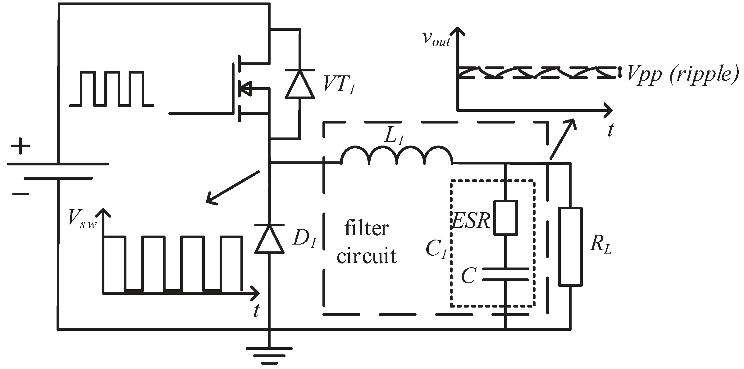
Figure 1 shows the principle of ripple generation in a common buck topology. That is, the high-frequency pulse-width modulation (PWM) signal causes voltage fluctuations of the same frequency, which cannot be completely filtered by the subsequent filter circuit, thus generating high-frequency ripple at the output. Due to the high frequency of the PWM, the impedance of the output AEC is almost equal to the impedance of its ESR at this frequency. Therefore, when the load is constant, the relationship between the ripple value and the ESR is approximately proportional, which indicates that the remaining life of the AECs can be easily obtained from ripple. However, in order to accurately measure high-frequency ripple, high-speed ADCs with sampling rates far exceeding the switching frequency must be used, which makes the relevant research not able to be applied to industrial applications such as built-in test (BIT) due to the high cost of data acquisition. Thus, it is of significance to focus on the technology of common low-cost, high-precision measurement of ripple wave.
When built-in test (BIT) is required for health monitoring based on ripple measurement, researchers always turn to other low-cost instruments. Therefore, several special ripple measurement schemes have been designed. Some studies focus on root mean square (RMS) measurements, one of which is to measure ripple by AC millivoltmeter [
25]. Le provides another scheme based on RMS-to-DC chips [
26]. Since the ripple voltage is not a standardized sinusoidal signal, the deteriorate degree of its spike could not be purely obtained by RMS measurement, thus the schemes above have not been widely applied.
Since ripple voltage could be measured by obtaining both peak and valley values, there exist various approaches to acquire the peak value. The well-known basic peak value detector is a solution convenient to implement; however, it is limited by bandwidth and is vulnerable to transient changes in tested SMPS. Some related studies have made improvements regarding. Jerry proposed an analogy peak measurement circuit, but it could not obtain the accurate value of ripple and only determined whether there was ripple beyond a fixed reference value [
27]. Zhou offered an implementation of ripple testing by specific peak detecting chips, but its low bandwidth increases measurement error [
28]. Smith proposed an improved peak measurement method by adding a high-speed comparator with open-drain output. It has the property of ameliorative accuracy at high frequency without diode, but it fails to acquire the valley voltage [
29]. Ren proposed a method to measure the peak-to-peak value of a periodic signal [
30]. In this scheme, the input periodic signal and a reference signal from a digital-to-analog converter (DAC) constitute both inputs of the comparator, whose output is captured by an MCU used for adjusting the DAC value by a binary search method. After multiple operating cycles, the DAC output could gradually approximate to the peak or valley values of the input signal. But it is only designed for power frequency AC measurement; in this case, the convergence is too slow. The authors did not conduct either simulation or practical experiments.
Under constant load, the SMPS output ripple can be regarded as a periodic signal. This paper proposes some improvements and realizes low-cost peak-to-peak ripple measurement. The contributions of this study include: the design of the ripple measurement system, the analysis of the measurement error, and the proposal of an optimization algorithm with a higher convergence speed according to the shape characteristics of the ripple signal. The experimental results indicate that the measurement error of this designed system is less than 0.5% with 20 ms consumption where the ripple value is larger than 500 mV, which completely satisfies the requirements of engineering applications and scientific research.
2. Ripple Measurement Scheme and Error Analysis
The ripple value of SMPS could be acquired by an expensive high-speed ADC. However, the high price makes it difficult to apply in BIT. This study provides a new scheme to cut down the expense by replacing the ADC with two high-speed comparators and adding a DAC to generate the reference voltage (one DAC is capable of measuring the peak and valley of a ripple at different moments and one high speed comparator is also enough with utilizing an analog switch). This method ensures accuracy with cost reduction. The designed ripple measurement system consists of four modules: high-pass filter (HPF) circuit, peak measurement, valley measurement, and MCU feedbacks. The block diagram of ripple measurement and the inner signals of peak measurement are shown in
Figure 2. And the waveforms of key nodes are shown in
Figure 3.
Figure 3c shows that the input signal originating from the output of the SMPS contains a high DC bias and an AC ripple. In the first step, an HPF is used to filter out the DC component. Ideally, the high-frequency ripple signal is hardly affected, while the DC voltage is completely eliminated. The filtered ripple voltage is shown in
Figure 3b.
The workflow of the measurement system is somewhat similar to the ADC with a successive approximation register (SAR). Each measurement requires several feedback cycles for convergence. During a certain feedback cycle, as illustrated in
Figure 3a, the DAC output voltage is constant and combines with the ripple signal to compose the input of the high-speed comparator. When the DAC output is lower than the peak, the high-speed comparator provides a periodic pulse, as shown in
Figure 3d, otherwise it remains low (this situation is not shown in
Figure 3). Once any periodic pulse is captured by the MCU, it increases the DAC output to approximate the peak. Otherwise, it drops the DAC value. The MCU repeats the above procedure until it cannot capture the pulse exactly, when the output of the DAC is highly equal to the peak voltage of the ripple.
As shown in the block diagram, the measurement system mainly includes an HPF, high-speed comparator, and DAC (with its reference source). The circuit design and the error analysis of each part are introduced below.
2.1. High-Pass Filter (HPF)
The HPF is used to block the DC component of SMPS. However, before the DC-blocking capacitor
C1 has been charged, the high DC voltage may damage the comparator and MCU. Therefore, the protection diode
D1 should be added. In order to provide a discharge path for
C1 after the input switches off, the resistor
R1 should be placed in the circuit. The modified HPF diagram is shown in
Figure 4a.
By setting the component values properly, the input DC element can be completely filtered out, while the AC element can be fully reserved. However, as
Figure 4 demonstrated, the parasitic parameters such as the input impedance of the subsequent high-speed comparator and the parasitic capacitance of the protection diode would introduce a small attenuation to the input signal. Since the impedance of
Ri is much larger than that of
Cj and
Ci, the HPF transfer function would be approximately expressed as follow
where
The high-pass filter
δhpf is independent of frequency, hence the peak value of the input voltage
vip and the peak value of the filtered signal have similar expressions compared to Equation (
3)
Since the exact values of Cj and Ci are difficult to obtain, the system error of the HPF circuit is hard to correct and is added in δhpf, which get its maximal value when C1 turns to minimal and Ci and Cj to maximal.
2.2. High-Speed Comparator Circuit
The measurement error caused by the comparator mainly includes two aspects: one part is affected by the frequency of the input signal and the bandwith of the comparator, and the other is derived from the manufacturing characteristics of different input transistors of comparators, which may not be exactly matched. By choosing the high-speed comparator with a cut-off frequency much higher than the ripples’, the error caused by the ripple frequency can be ignored. Then the latter component, which is represented by the input offset voltage voffset, can be considered as the dominated error.
The two input signals of the comparator come from the DAC and HPF, respectively. Each filtered signal peak
vcp corresponds to a threshold point. If the DAC output crosses the point, the comparator output flips.
where
2.3. DAC Circuit
The digital signal from the MCU is converted into analog quantity by a DAC, which requires a input reference voltage (
vref) to operate properly. Given a digital signal M, the ideal output voltage of a DAC is
Since
M is a discrete value,
vdac_ideal may not be totally equal to
vth. Given the assumption that
then
M is the integral part of m, and hence it generates quantization error
δq.
where
The conversion accuracy of the DAC circuit is affected by a series of factors. For example, the input reference voltage (
vref) is generated by a reference source with a subtle error. The DAC characteristics such as integral nonlinearity and DAC differential nonlinearity also reduce the accuracy. Generally, the DAC error is 2 or 3 times its least significant bit (LSB). Let
N stand for the number of DAC bits and
K stand for the LSBs of the DAC error. The DAC output
vdac would be derived as follows:
where
2.4. Total Error
When the digital signal
M meet the threshold point, the measure ripple
vm could be calculated by:
On the basis of Equations (
4), (
8), (
12), (
15), and (
16),
Since
,
,
,
, and
are much smaller than 1, the total error could be approximately expressed as
where
In the valley measurement, in order to generate a negative reference voltage, the DAC output is processed by a subtractor that contains an operational amplifier (OPA). In this study, the error of a high-precision OPA with an offset voltage is much smaller than the error of the selected high-speed comparator, hence the subtractor error could be negligible.
Referring to Equations (
8) and (
12), the total measurement error is related to the ripple amplitude. The larger the ripple value is, the smaller the measurement error. In the case that the ripple is too small, a special amplifying circuit is required, which is not mentioned in this paper.
Consider the traditional measurement scheme, i.e., using a high-speed ADC to directly sample the HPF output signal. Similar to the derivation of Equation (
20), the measurement error of a high-speed ADC scheme can be described as follows:
where
,
,
, and
have similar expressions to Equations (
4), (
12), (
15), and (
16), respectively. But high-speed ADC is generally with 8 or 10 bits, which is less than the slow-speed DAC, leading to a greater quantization error
and ADC internal error
. The exact value of the errors will be further discussed in the section on experiment verification.
3. Ripple Waveform Analysis
The measurement error of this design is determined by the components, and the measurement speed can be improved by using some prior information. In some applications, such as predicting the remaining life of SMPS by ripple value, the information about the topology of SMPS and the ripple waveform characteristics are already known, which can contribute to the feedback cycle reduction. This paper takes the typical buck converter topology as an example. Its output ripple can be approximated as a triangular wave in continuous current mode (CCM). Then the output signal of an HPF can be described as follows:
where
and
are the minimum and maximum value of
, respectively,
T is the switching period of the SMPS to be measured,
D is the duty ratio, and
and
are the rising and falling slopes of the approximated triangular wave, respectively. Since
has only AC components, the triangular waves are symmetrical, and the ripple signal is periodic, we can obtain following expressions:
Referring to Equations (
22)–(
25), we can obtain
Moreover, the mathematical expression of the comparator output is as follows:
where
and
are the comparator’s noninverting and inverting inputs, respectively. The comparator can produce a square wave under the condition that Equation (
28) is satisfied. Otherwise, it either remains high or remains low.
The square wave in a single cycle is described as follows:
In combination with Equations (
22)–(
29), the high duration
th of the output signal is derived as follows:
If the DAC’s two output values
and
both satisfy Equation (
28) and their corresponding high-level durations are
and
, they correspond to the relationship
Equation (
32) means only two cycles are required for the peak measurement of buck topology, but it is not recommended that it be directly applied because it enlarges the measurement error. The practical measurement algorithm will be discussed in the next section. The principle of valley measurement is similar to peak measurement, and the details will not be described here.
4. Algorithm Design
In order to converge the DAC output to the ripple peak rapidly and accurately, the MCU should capture the output pulses of the high-speed comparator and adjust the DAC output according to a certain method. For example, binary search is an available algorithm that updates one DAC bit at each iteration to narrow the search region. Hence, the iterative cycles are equal to the DAC bits, that is, the higher DAC accuracy it achieves, the greater number of iterations it costs. The required time for an iteration contains three parts: pulse capturing, instructions transmission, and setting time of DAC output. The first is the dominant cost, which is always several dozen times higher than the ripple period for reducing the random error. Therefore, a faster measurement can be realized by reducing the cycle number or cutting the waiting time in each iteration. According to Equation (
32), only two measurements are necessary to calculate the peak voltage. However, there is an estimated error since the ripple is not completely equivalent to the triangular wave and the pulse width measurement also introduces quantization errors. Therefore, a new algorithm based on the triangular wave approximation and the binary search is proposed here. The algorithm not only improves the convergence speed but also guarantees measurement accuracy. Firstly, the algorithm estimates the approximate peak value by two measurements. Secondly, the algorithm determines the upper and lower bounds of the peak in the vicinity of the estimated value. Finally, the binary search is used to ensure the converge of DAC output to the peak of the ripple. The flowchart is shown in
Figure 5, and the details of three steps are introduced below and shown in
Figure 6.
4.1. Step 1. Estimate the Peak Value by Two Measurements
According to Equation (
32), two sets of measurement data that satisfy Equation (
28) are required for peak estimation. The first set can be accessed by taking DAC output as the average of ripples (zero, in most cases). In order to obtain the second data set, an appropriate DAC output should be selected. If it is too small, the estimated error will be quite large; when it is too large, Equation (
28) is not satisfied. Therefore, we take 1/8 of the scale range of DAC output in the initial attempt. If it is still larger than the peak value, then we continue to take another 1/8 of the last output until the pulse signal is captured. When the ripple is small, the convergence speed of the algorithm is three times of the traditional binary search. Then the MCU calculates the ripple peak after obtaining two sets of measurement data.
4.2. Step 2. Determine the Upper and Lower Bounds of Binary Search from the Estimated Value
The DAC output is set to the estimated value of step 1. If the estimated value is lower than the ripple peak, the MCU can receive pulses from the comparator briefly. At this time, the above estimation value can be set as the lower bound of the binary search. Otherwise, the upper bound is acquired. When the lower bound has already been determined, an empirical constant (for example, 50 mV) is added to the lower bound as the upper bound. If the value is still smaller than the peak, the MCU then sets the DAC output as the new lower bound and iterates the process until the MCU fails to capture the comparator output pulse. In general, the upper bound could be determined without repeated iterations. The upper bound is determined in the calculation process, which is similar to the case shown above in
Figure 5.
4.3. Step 3. Determine the Peak Value based on Binary Search
When the lower and upper bounds are all determined, the binary search method can be applied to obtain the DAC output. The DAC output is firstly set to the average value of the two bounds. During each measurement, if the MCU receives feedback pulses, which means the current DAC output is smaller than the peak value of the ripple, the lower bound should be updated to the output of the DAC. Otherwise, the DAC output is too large and the upper bound should be updated. The above process is repeated until the distance of both bounds is smaller than the tolerance, then we eventually obtain the ripple voltage.
The differences in peak measurement between binary search and the proposed method are shown in
Figure 6. Generally, Step 1, Step 2, and Step 3 take 2 or 3 cycles, 2 or 3 cycles, and 4 or 5 cycles, respectively. It is obvious that the required time will be significantly reduced. As previously mentioned, the waiting time in each cycle can be several dozen times of the period of a ripple to ensure a high measurement accuracy. Since the first several cycles only aim for a narrow search area rather than high accuracy, less time (one-quarter of an accuracy cycle) can be allocated in these cycles. As
Figure 6 shows, when the shape of a waveform is used in ripple estimation, the measuring time is about three quarters of the binary search method. On this basis, it can achieve a shorter measurement time by cutting down the waiting time in the first several cycles because the results of the first several cycles are only used for peak estimation with lower accuracy requirement. The process of valley measurement is similar to peak measurement; therefore, the details are not described here.
5. Experimental Verification
In order to prove the characteristics of the proposed scheme, a print circuit board (PCB) was designed for verification. The prototype is demonstrated in
Figure 7 and the major components are described in
Table 1. The theoretical error calculated by Equation (
20) is shown in
Table 2 and is compared with the error of traditional ADC measurement calculated by Equation (
21) (assuming that the internal error of the 8-bit, 10-bit, and 12-bit ADC is 1, 2 and 3, respectively). The results are shown in
Figure 8.
From
Figure 8, we see that the error of the prototype based on proposed method is even smaller than that of the 12-bit high-speed ADC (for the measurement of small signals, an amplification circuit is necessary to lower quantization error and improve measurement precision, which is not considered in ADC error calculation). In fact, when the ripple amplitude is above 100 mV, the theoretical error of the prototype is under 1%, which has an advantage over the majority of oscilloscopes (vertical accuracy between 3–5%). Due to the lack of high-accuracy ripple measurement equipment, it is difficult to calibrate the actual measurement error of the prototype. Here, we use another alternative, i.e., utilizing a WAVESURFER10 oscilloscope with 1% DC vertical error to carry out the comparison experiment.
The experimental environment is shown in
Figure 9. The DG1022U signal generator is used to generate triangular waves of different amplitude, frequency, and duty ratio. The peak-to-peak value is measured simultaneously by the WAVESERFER 10 oscilloscope and the prototype. The measurement results are displayed on the screen and sent to the computer for data storage. The differences in measurement results between the WAVESURFER 10 oscilloscope and the designed prototype are shown in
Figure 10,
Figure 11 and
Figure 12. Since the theoretical error of the selected oscilloscope is larger than the designed prototype, the vertical axis is the “absolute difference” instead of the “measurement error”.
Figure 10 demonstrates that the absolute differences in measurement between the two methods are 1 mV (5%) and 1 mV (2%), respectively, for the 20 mV and 50 mV ripples, which is in accordance with the theoretical calculation shown in
Table 2 (with consideration of the oscilloscope error and resolution, for example, the minimum resolution of oscilloscope is 1 mV). The absolute difference in measurement results remains 2 mV (2%) in response to the input of a 100 mV ripple, which possibly is the maximum error from the test equipment and oscilloscope simultaneously, along with opposite error symbol. Of course, it is also possible that the actual measurement error at this point is greater than the theoretical value. When the ripple is over 100 mV, the result of the two instruments is vicinal (the measurement difference is below 1% of the ripple).
Figure 11 shows a slight difference between absolute errors in measurement results for different duty ratios (less than the resolution ratio of the oscilloscope in this range, 3 mV).
Figure 12 illustrates the capability of the proposed measurement system for ripples up to 500 kHz.
The above experiments support the following conclusions:
- (1)
When the ripple amplitude is under 100 mV, the measurement error of the prototype is consistent with the theoretical value and smaller than the measurement error of the general oscilloscope (5%).
- (2)
When the ripple amplitude is larger than 100 mV, the measurement error of the prototype is also not smaller than the professional oscilloscope (1%).
- (3)
The measurement precision of the proposed system is hardly affected by the variation of both frequency and duty ratio, which indicates that the designed system can be utilized in extensive field applications.
Since the period of the ripple is usually less than 0.1 ms, the measurement period was set to 3 ms in the experiment. Experimental results show that if a triangular wave is used as the input signal, the ordinary binary research method takes 40 ms, the improved method takes 28 ms, and if the waiting time of the first few cycles is reduced, it only takes 20 ms. In addition, the above methods have the same measurement error. The experimental results are consistent with the theoretical analysis (
Figure 6), and the results indicate that the measurement speed can be doubled using the improved method, which is useful in some data-driven applications.
6. Conclusions
Ripple acts as one of the crucial parameters of SMPS, reflecting the operating health status. This manuscript presents a new ripple measuring scheme that utilizes inexpensive a low-speed DAC and high-speed comparators, instead of costly high-speed ADCs, and is also characterized by low cost, high precision, portability, and automation. The operating details and error sources are described, and a new advanced strategy for ripple measurement cycle reduction is proposed. Both the theory and experiment show the designed measurement can be utilized in extensive field applications, including the measurement of ripple under different amplitudes, frequencies, and duty ratios.
Due to the limited cost, the health management of SMPS is mainly realized by monitoring the voltage and current of the system. In this paper, the ripple value can be obtained at a low cost, so as to promote the implementation of relevant studies on the health management of SMPS using ripple. This is of great significance for detecting potential problems in power system operation and preventing sudden failure accidents. Moreover, the high precision and automation of the proposed method enables it to be widely applied for the quality testing of SMPS and other engineering fields.


