Abstract
A surface-potential-based analytical I-V model of single-gate (SG) silicon-on-insulator (SOI) MOSFETs in full-depletion (FD) mode is proposed and compared with numerical data and Khandelwal’s experimental results. An explicit calculation scheme of surface potential, processing high computation accuracy and efficiency, is demonstrated according to the derivation of the coupling relation between surface potential and back-channel potential. The maximum absolute error decreases into 10−7 V scale, and computation efficiency is improved substantially compared with numerical iteration. Depending on the surface potential, the drain current is derived in closed-form and validated by Khandelwal’s experimental data. High computation accuracy and efficiency suggest that this analytical I-V model displays great promise for SOI device optimizations and circuit simulations.
1. Introduction
Silicon integrated circuits (ICs) have become increasingly dense because the feature size of MOSFETs based on silicon-on-insulator (SOI) structure has not been a constraint in the sub-nanometer scale and both performance and cost improve as the feature size decreases. Up to now, there has still been considerable interest in optimizing properties of SOI MOSFETs [1,2,3] due to the widespread applications of SOI MOSFETs, such as sensors [4], memories [5], millimeter-wave circuits [6], and so on. Therefore, both device property optimization and IC design in the different fields imply that an analytical I-V model for accurately predicting I-V characteristics of SOI MOSFETs is imperative.
Recently, several analytical I-V models for bulk MOSFETs have been reported in the literatures [7,8,9,10,11] based on threshold voltage [7], inversion charge [8], and surface potential [9,10,11]. These models are demonstrated on the condition that the devices work in the partial-depletion (PD) mode, i.e., back-channel potential can be assumed to equate to zero or channel potential. However, these models cannot be applied into full-depletion (FD) single-gate (SG) SOI MOSFETs without any adjustment, due to the strong back-to-surface (B-S) potential coupling effect introduced by the ultrathin-body and buried oxide (BOX) in the FD SG SOI MOSFETs. Such a coupling effect increases the calculation complexity. In the meantime, some models [12,13,14,15] of multiple-gate SOI MOSFETs have been proposed, and some models of FD SG SOI MOSFETs [16,17,18,19,20] incorporating the B-S potential coupling effect are derived. Ravariu et al. [16] and Pandey et al. [17] developed threshold models for long- and short-channel FD SG SOI MOSFETs, respectively, by numerically solving a complicated equation about the position of the minimum back-channel potential. M. Miura-Mattausch et al. [18] also proposed an analytical I-V model of FD SG SOI MOSFETs based on a completely potential-based description solving the Poisson’s equation iteratively together with additional equations. Here, numerical computation reduced the calculation efficiency. W. Wu et al. [19] and Y. S. Yu et al. [20] gave surface-potential-based analytical I-V models in which smoothing functions are employed. In addition. J. Huang et al. [21] described a DC model of FD poly-Si TFTs based on the assumption of B-S potential relation. Because of computation complexity, they gave up deriving B-S potential relation, leading to low computation accuracy.
In this paper, we propose a surface-potential-based analytical I-V model of FD SG SOI MOSFETs. An explicit solution of surface potential in FD SG SOI MOSFETs is solved from the 1-D Poisson’s equation and derivation of B-S potential coupling relation. This surface potential calculation scheme has high computation accuracy and efficiency, which is verified by numerical techniques. Subsequently, based on the surface potential, we present the drain current analytically and validate it with Khandelwal’s experimental data [22]. Finally, combining with simulation results of this model, we discuss the effects of the different parameters on the electrical properties of FD SG SOI MOSFETs in detail.
2. Surface Potential Explicit Calculation Scheme
For FD SG SOI MOSFETs, a crystalline silicon (c-Si) film is deposited on a BOX film, as shown in Figure 1. The x-axis is perpendicular to the plane of gate, the carrier transport occurs along the y-axis, and the z-axis is set parallel to the structural confinement direction. In addition, tox and tsi are gate oxide and silicon body thicknesses, respectively. Following the gradual channel approximation and neglecting the whole concentration, we can simply write the Poisson’s equation as:
Here, φ is the electrostatic potential as a function of the variable x, the free charge density is demonstrated as where Vt is the thermal voltage (kT/q), k is the Boltzmann constant, T is the absolute temperature, q is the magnitude of electronic charge, εsi is the dielectric permittivity of silicon, n0 is expressed as , Vch is the channel potential, Vfp is the quasi-Femi potential, and the doping concentration is symbolled by Na. According to Figure 1, there are three boundary conditions for (1), i.e., φs is the surface potential with φs = φ(tsi), φb is the back-channel potential with φb = φ(0), and (dφ/dx)x=0 = 0.
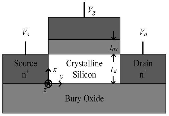
Figure 1.
x-y cross section of silicon-on-insulator (SOI) MOSFETs.
It is noted that the c-Si film thickness of SOI MOSFETs comes into a sub-nanometer (<100 nm) scale so that the devices work in the FD mode rather than the PD mode of the bulk MOSFETs. From device structure aspect, the sub-nanometer film on BOX results in the strong back-to-surface (B-S) potential coupling effect, implied by the boundary condition φb = φ(0) for (1). Here, φb cannot be set as a constant equating to Vch, actually it is a function as φs according to φs = φ(tsi). This function is the B-S potential coupling relation, which is to be derived as follows.
For FD SG SOI MOSFETs, the channel layer is usually in the lightly or moderately doped case, i.e., free charge density is far larger than Na, yielding:
We can observe that the mathematical form of (1) is relatively complicated because of the inclusion of an exponent term and a constant term in the right-hand side (RSH) of the equation, so that a solution of φ cannot be solved generally up to now. However, (2) retains the clear physical meaning and becomes the simplification of (1) to help us analytically derive the B-S potential coupling relation. We integrated (2) twice to obtain this relation as:
Here, LD is the Debye length with LD = (εsiVt/2qn0)1/2.
Using the Gauss’s law, the relation , and (1), we can obtain the implicit function of φs as:
If φb is set as a constant with φb = Vch, then (4) degenerates to be only suitable for PD MOSFETs, i.e.,
In the PD mode, we can solve (5) only to get φs. However, in the FD mode, we should analytically solve the equation set of (3) and (4) to get the expressions of φs and φb. Obviously, there is much more computation complexity in the FD mode compared with the PD mode. Substituting (3) into (4), we can solve an explicit solution of φb as:
where β is symbolled as , F is symbolled as , r is the nature parameter with , and W0 is the Lambert W function [23], which is the solution of W0(x)exp[W0(x)] = x. Furthermore, substituting (6) into (4), we can derive the explicit solution of φs as:
Here, λ is the bulk factor with , D can be considered as the impact fact describing the B-S potential coupling effect in FD SG SOI MOSFETs with , and ω is the Schroder series [24] used to improve the accuracy of the explicit solution of φs with . Here, , and y’ and y’’ are the first and the second derivatives of y versus φs, respectively.
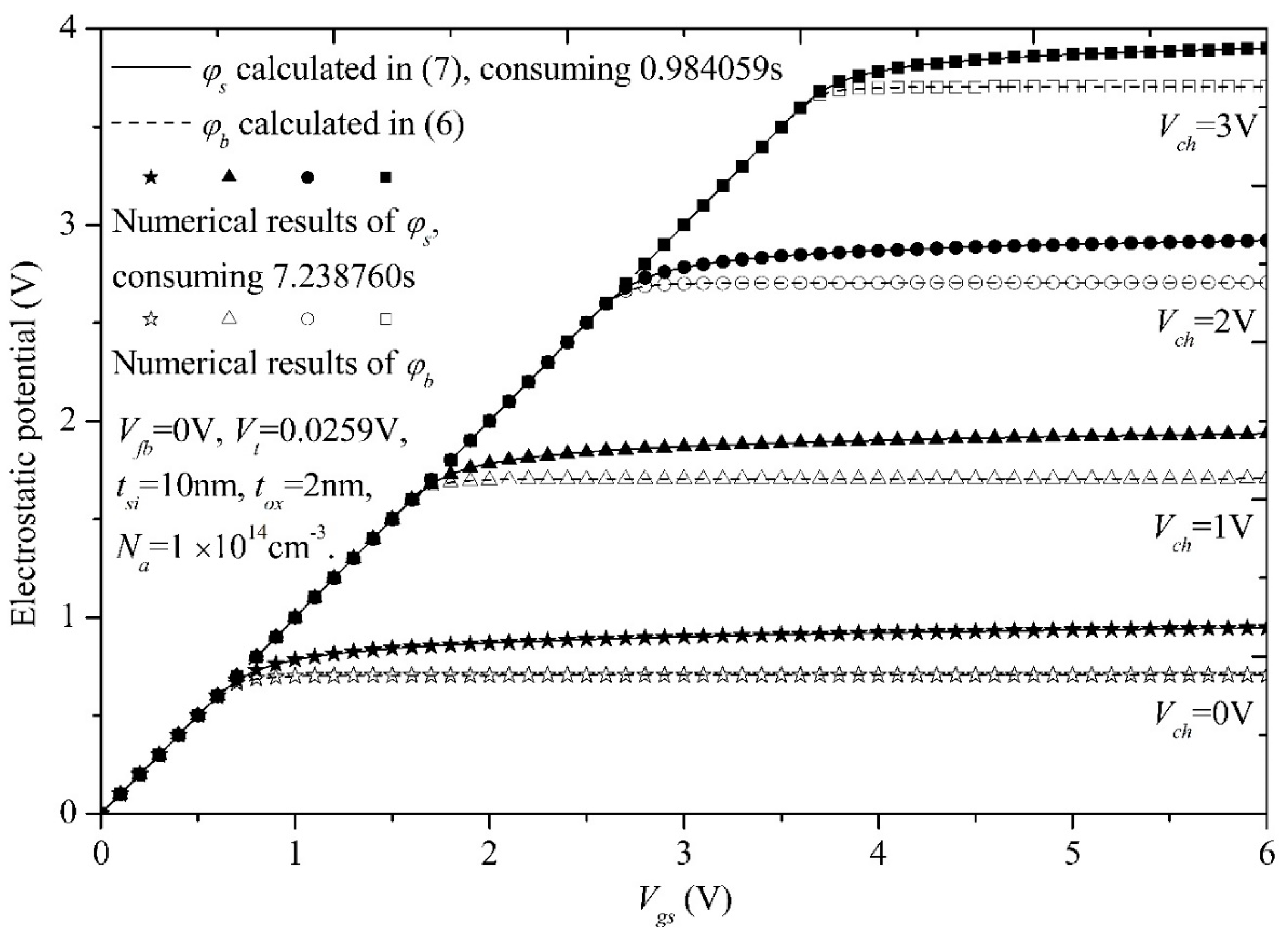
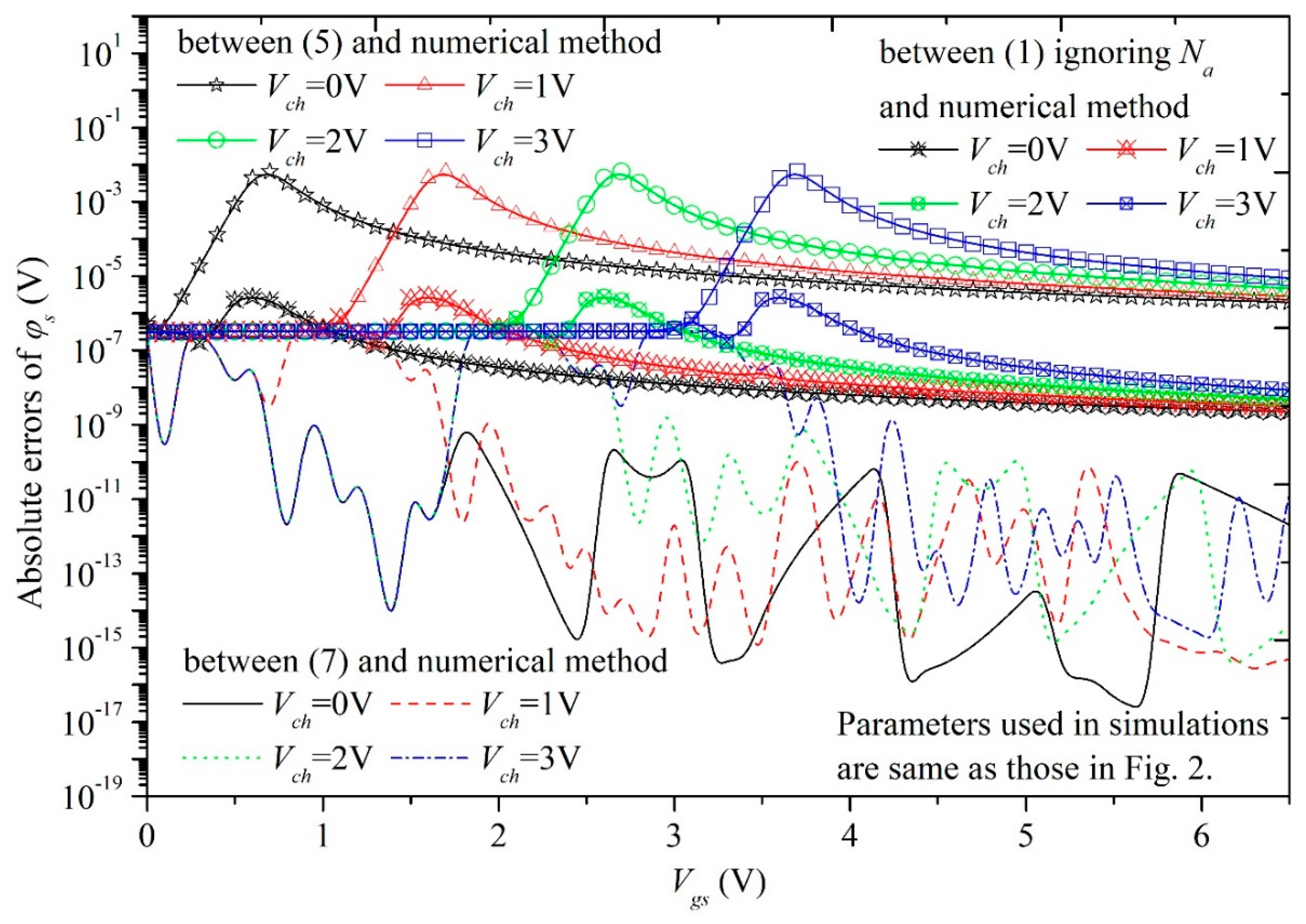
We compare φs of our scheme with that of the numerical method and show the results in Figure 2 and Figure 3. We observe that good agreements are obtained and computational efficiency of (7) is seven times that of the numerical method, as shown in Figure 2. Moreover, we analyze the absolute errors of φs in the different cases compared with the numerical results of (4) in Figure 3. First of all, the maximum errors of φs between (7) and the numerical results are less than 10–7 V. Then, the models of PD MOSFETs, i.e., (5), cannot be adopted into FD SOI MOSFETs and errors are up to 0.01V, because φb cannot be set as a constant in the FD mode. Lastly, in the process of computing φs, Na should not be ignored even if in the lightly or moderately doped case, or else large errors woule be introduced into the models.
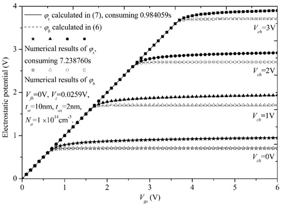
Figure 2.
Comparisons between the surface potential scheme and numerical results for different Vch.
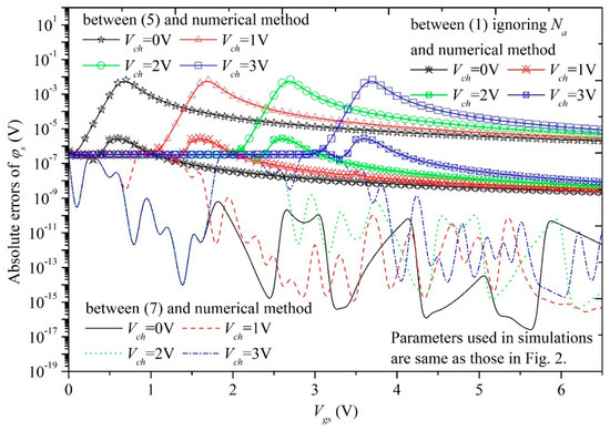
Figure 3.
Absolute errors of φs between solution and numerical method vs. Vgs.
3. Analytical I-V Model
Considering the single-gate structure of the devices, the charge-sheet model (CSM) [25] derived by Brews can be adopted to derive the drain current including the drift and diffusion components, i.e., Ids1 and Ids2, respectively. Based on the CSM and the solution of φs, we get the drain current Ids as:
Here, φss and φsd are solutions of φs corresponding to Vch = 0 and Vch = Vds, respectively, and Qi is the free charge density per unit area, which can be derived by using the Gauss’s law at the interface between oxide and channel layers, yielding:
In (8), μ is a typical set of universal effective charge mobility [26], including acoustical phonon [27] and surface roughness [28] scattering of the inversion layer carriers influenced from the normal field, i.e.,
where μ0 is the maximum extracted value of the mobility at a given doping concentration, and θ1 and θ2 are degeneration parameters introduced by phonon scattering and surface-roughness scattering due to Vgs.
Substituting (9) and (10) into (8), we can analytically solve the expression of Ids as:
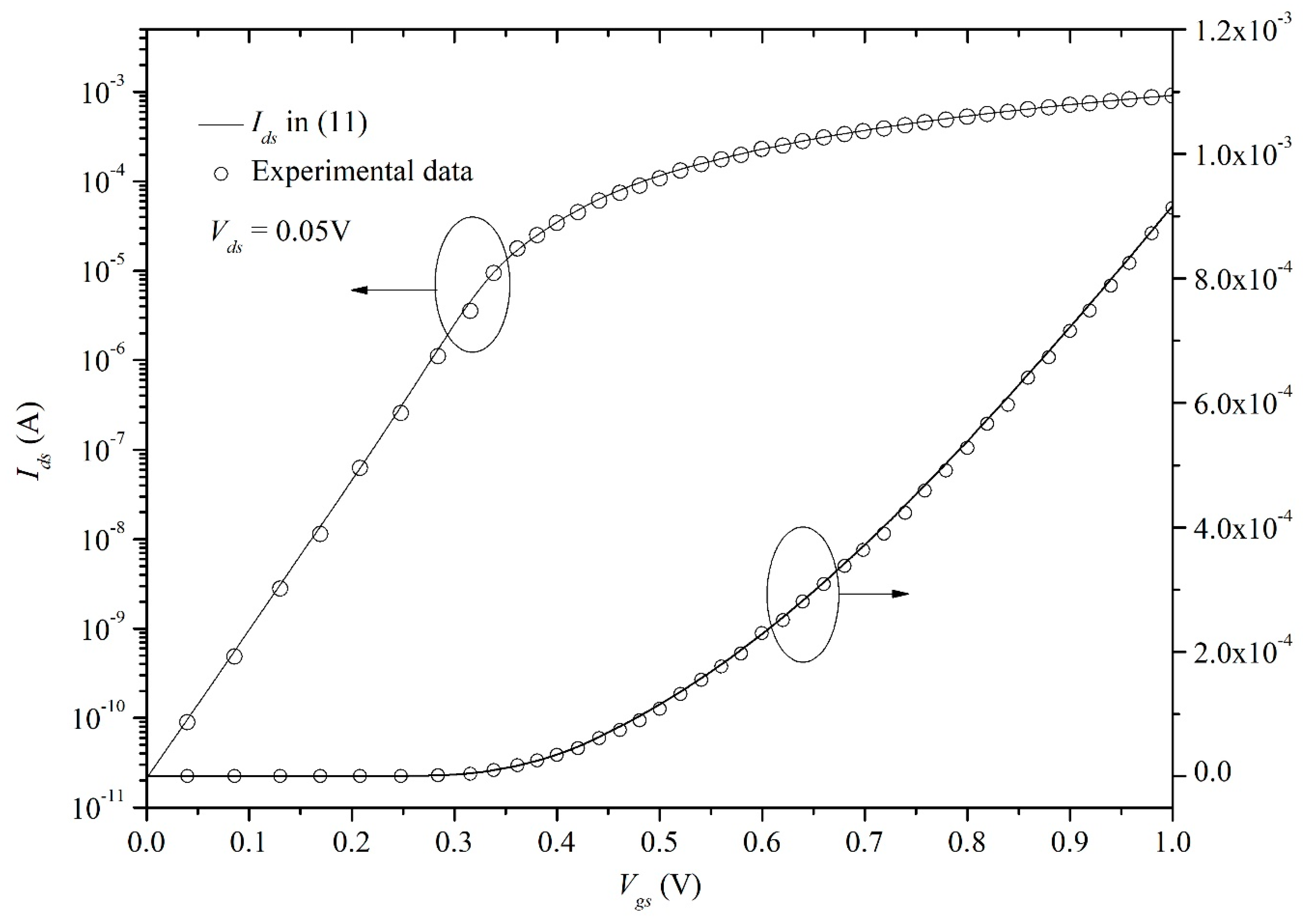
Furthermore, we match the results of (11) with Khandelwal’s experimental data [22] required from ultrathin-body SOI MOSFETs in the cases of long- and short-channels. In [22], the ultrathin-body SOI MOSFETs were manufactured, with a silicon body thickness of 8 nm and gate oxide thickness of 1.2 nm, respectively. For long-channel devices, the length of channel is 11 μm. For short-channel devices, the length of channel is 30 nm. The parameters used in the simulations are listed in Table 1. As shown in Figure 4, Figure 5, Figure 6 and Figure 7, we can observe that such a model can give a consistent solution for both transfer and output characteristics. It is noted that, for short-channel devices, channel-length modulation (CLM) is considered by using “effective drain-source voltage” [29] in our I-V model, i.e.,
In (12), the parameter a is a transition factor deciding shift from the drain-to-source voltage Vds to the effective drain-source voltage Vdseff, and Vdsat is an extracted saturation voltage parameter. In the process of the calculation, we can substitute Vdseff for Vch in (6) and (7) to make the model include CLM, which is equivalent with pinch-off behavior or velocity saturation.

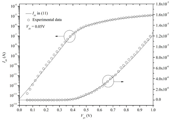
Figure 4.
Comparisons of transfer characteristics between our drain current model results and long-channel experimental data [22] from Khandelwal et al.

Figure 5.
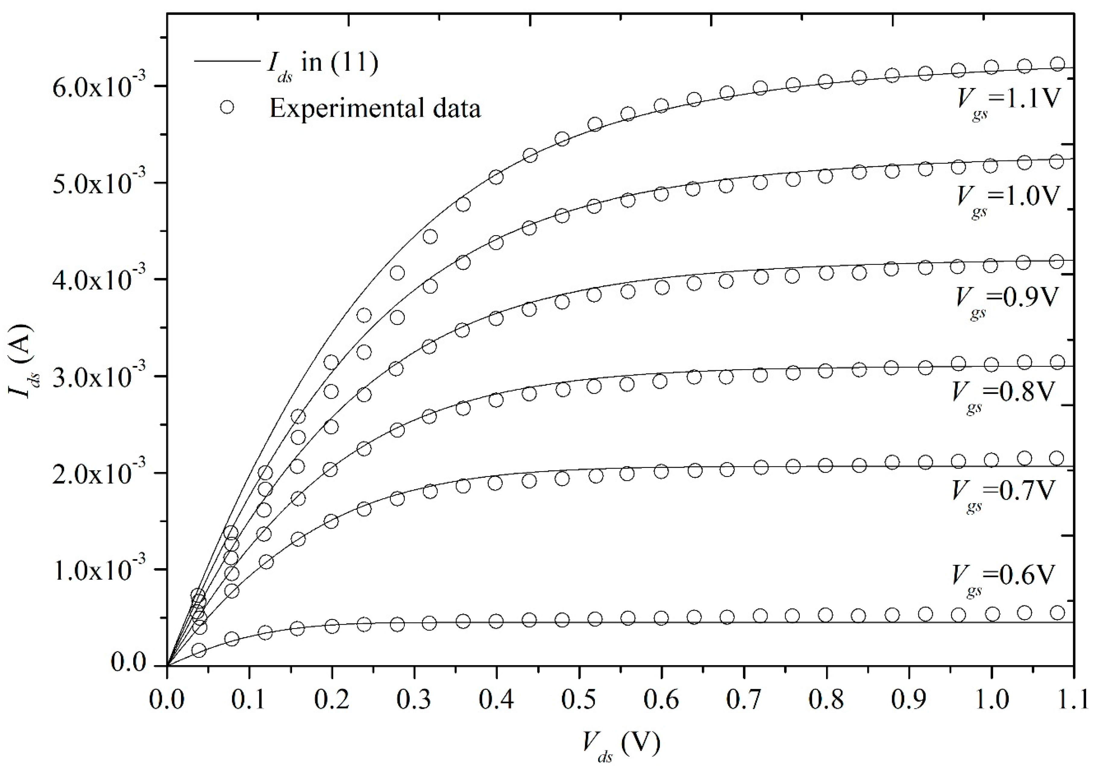
Comparisons of output characteristics between our drain current model results and long-channel experimental data [22] from Khandelwal et al.

Figure 6.
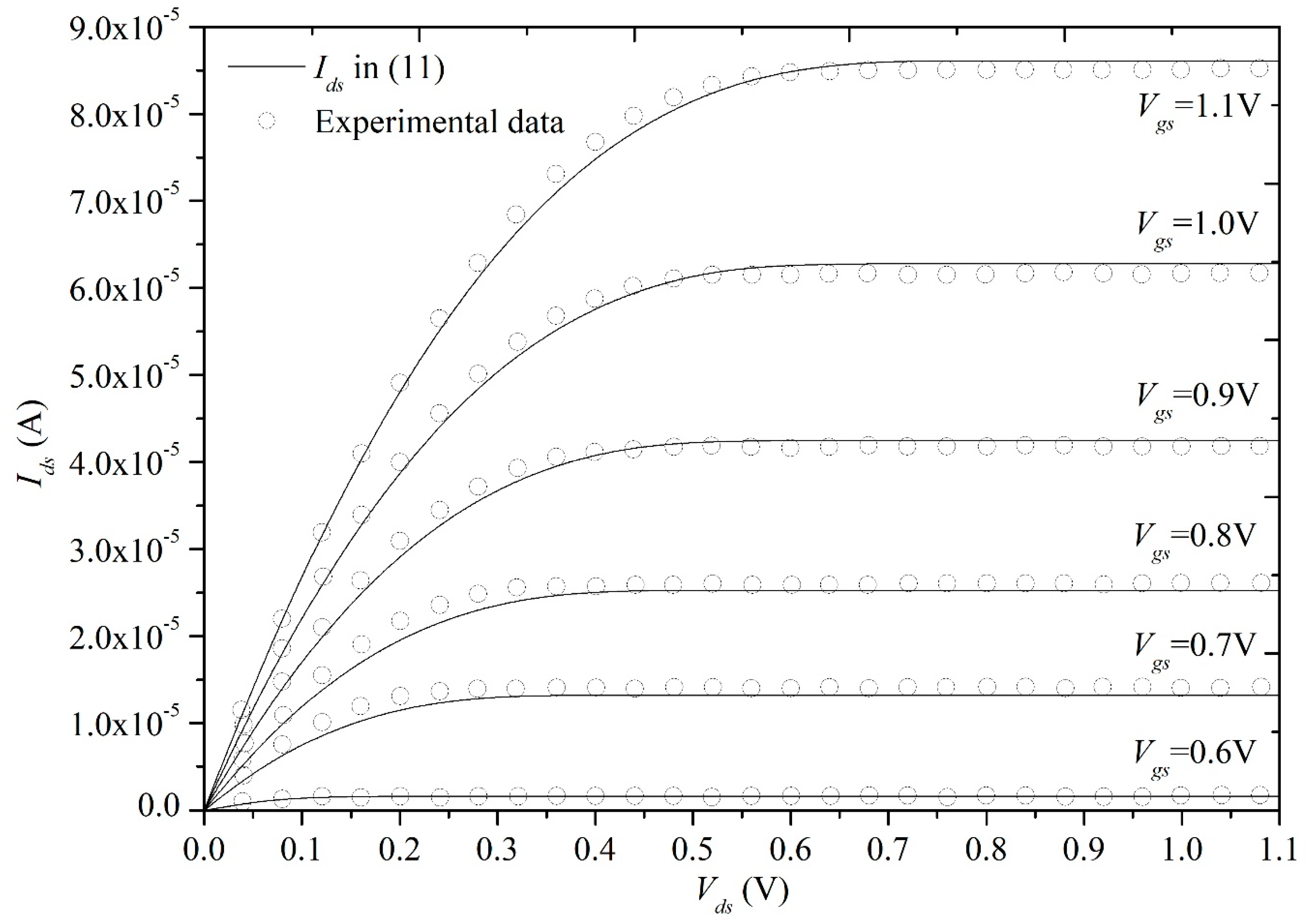
Comparisons of transfer characteristics between our drain current model results and short-channel experimental data [22] from Khandelwal et al.
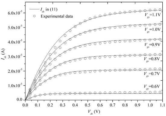
Figure 7.
Comparisons of output characteristics between our drain current model results and short-channel experimental data [22] from Khandelwal et al.
In Figure 4 and Figure 5, we compare the model with Khandelwal’s experimental data [22] for Ids–Vgs and Ids–Vds characteristics in the long-channel device with 11 μm, which does not have a significant presence of channel-length modulation (CLM) in its characteristics. The excellent agreement between the model and the experimental data validates the core drain current model for long-channel devices. In Figure 6 and Figure 7, our model is evaluated for short-channel effects by comparing Ids–Vgs and Ids–Vds characteristics against Khandelwal’s experimental data [22] for a short-channel device with L = 30 nm, which also demonstrate good model accuracy. The presence of CLM is apparent from Khandelwal’s experimental data [22] of output conductance (Figure 7) in this device. The reason why our proposed model can still capture these phenomena quite well is that we introduce “effective drain-source voltage” to describe CLM. According to the transfer characteristics shown in Figure 4 and Figure 6, we can observe that short channel effects lead to subthreshold property degradation and a larger leakage current. According to output characteristics shown in Figure 5 and Figure 7, we can observe that short channel effects result in obvious CLM or velocity saturation.
4. Discussion
In this section, we give some discussions about surface potential and drain current properties influenced by the structure parameters and the doping concentration of full-depletion single-gate SOI MOSFETs, including tox, tsi, and Na. The parameters used in the simulations are listed in Table 1. We analyze the effect from the single variable by using our model as follows.
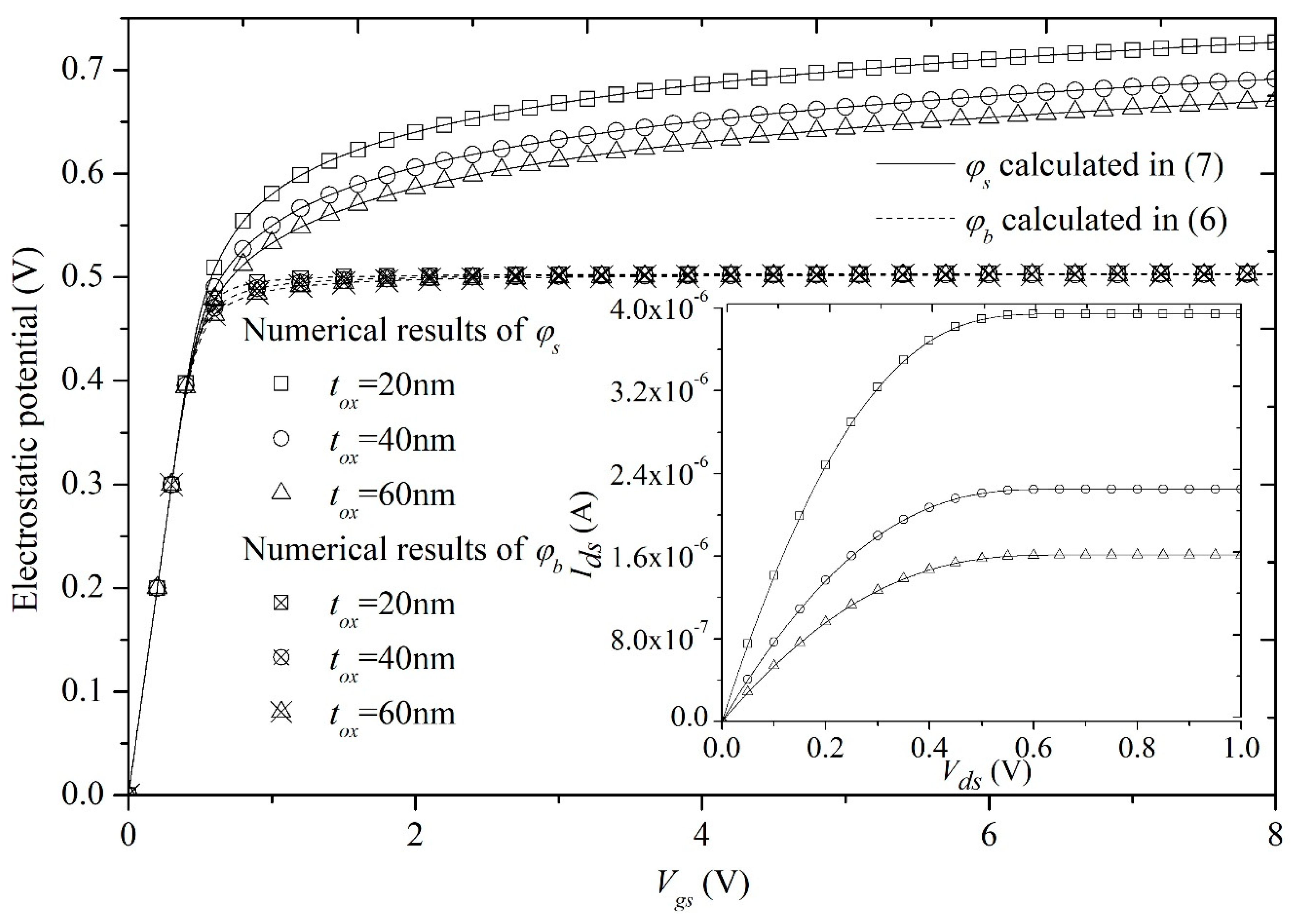
- The thickness tox of dielectric between gate and channel rightly determines the ability of inducing charges, particularly for the strong inversion region, as shown in Figure 8. We can observe that φs increases as tox decreases. Thin tox leads to larger Cox, and then, according to the Gauss’s law, many more free charges are introduced in the strong inversion region. It means that larger φs and Ids can be obtained in the channel.
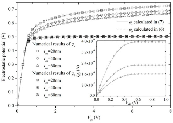 Figure 8. Comparisons between the surface potential calculation scheme and numerical results for different tox, and the drain current in (11).
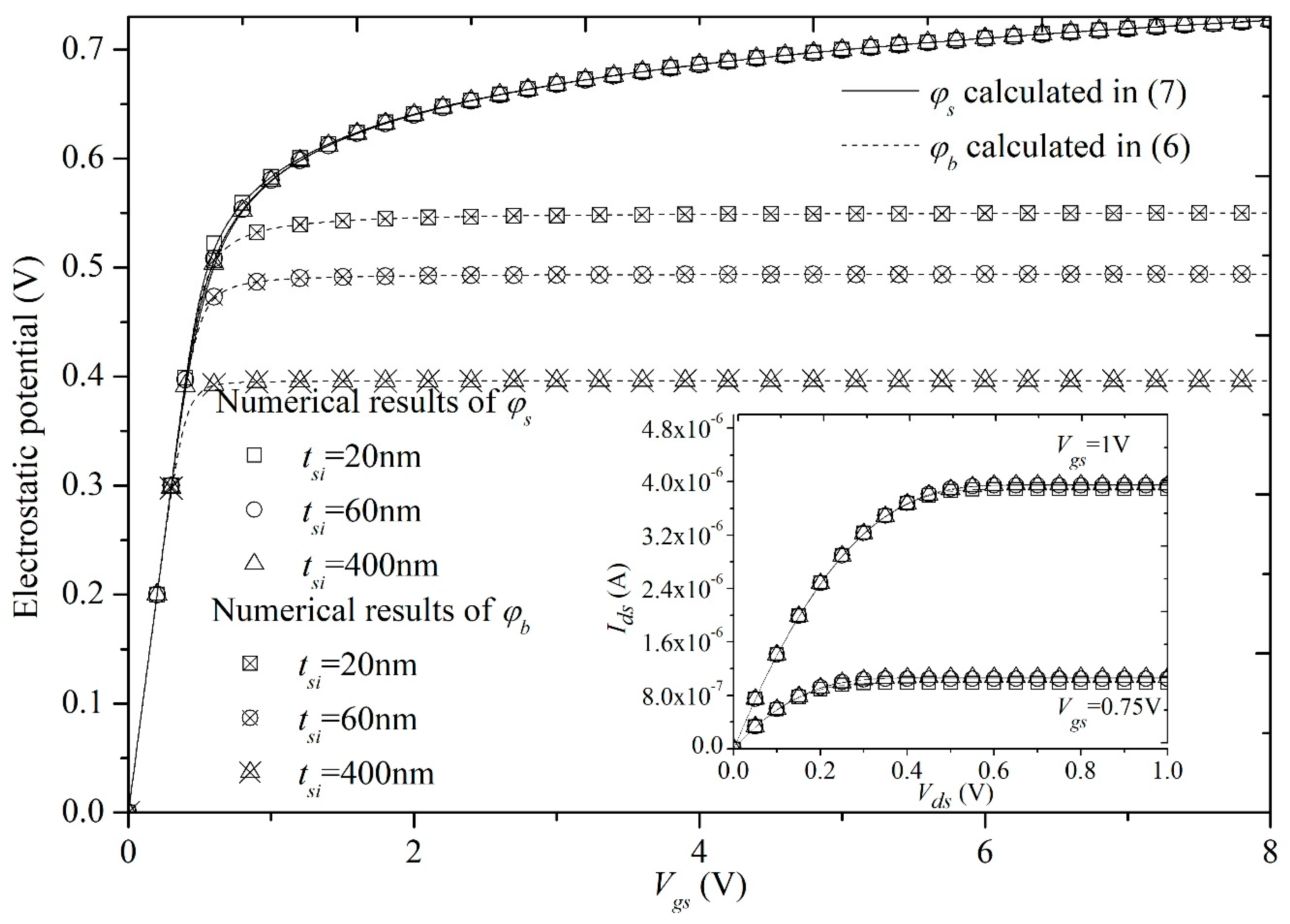
 - The thickness tsi of the channel film can influence φb but not φs. According to Figure 9, tsi is larger and φb becomes larger. It is implied by the simplified Poisson’s equation (1) only including the doping concentration. Simultaneously, Ids is affected by tsi lightly, because the free charges in the inversion layers are confined to a very thin layer with the order of 10–100Å [30]. That is also shown in Figure 9, graphed by our model.
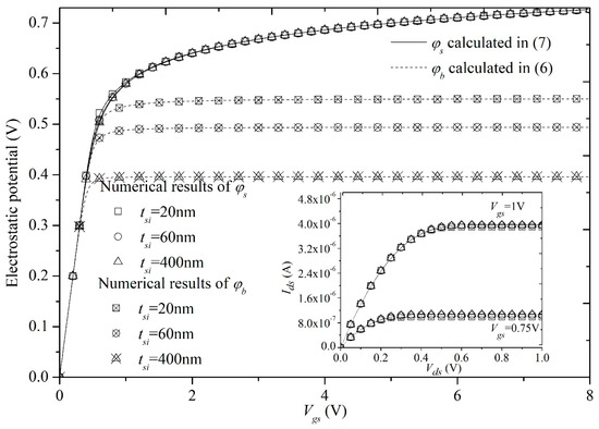 Figure 9. Comparisons between the surface potential calculation scheme and numerical results for different tsi, and the drain current in (11).
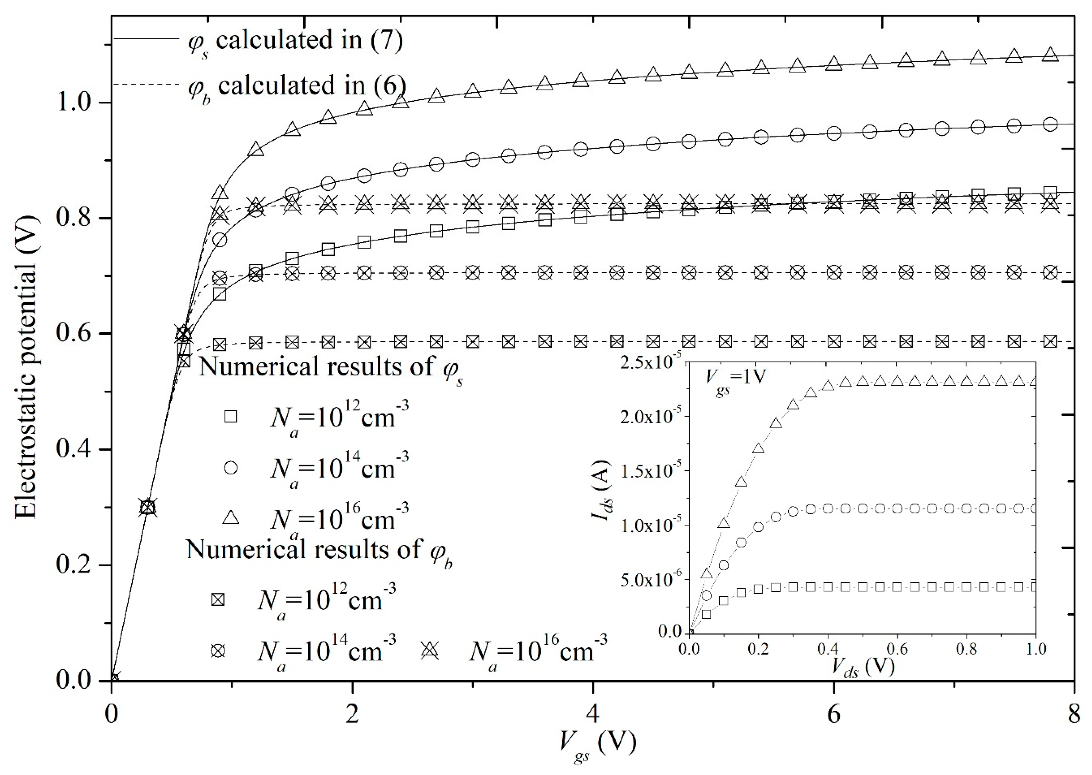
 - Finally, we can observe from Figure 10 that φs, φb, and Ids are in positive correlation with the doping concentration Na, because Na directly decides the value of the free charge density.
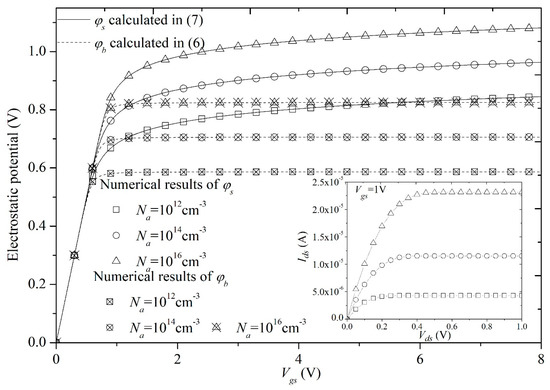 Figure 10. Comparisons between the surface potential calculation scheme and numerical results for different Na, and the drain current in (11).
5. Conclusions
In this paper, we provided a surface-potential-based analytical I-V model for full-depletion single-gate silicon-on-insulator MOSFETs with lightly or moderately doped channels. Based on deriving analytically the back-to-surface potential coupling relation, we solved the explicit solution of the implicit surface potential function by using the Lambert W function, and matched this solution with the numerical iteration method. Considering single-gate structure and ultrathin channel film, the drain current was derived analytically on the basis of the charge sheet model, and good agreements with experimental data were obtained. Finally, we gave the discussions about influences of the structure parameters and the doping concentration on the electrostatic properties of the devices. As a result, accurate simulation results demonstrate that our model can predict electrostatic properties of full-depletion single-gate silicon-on-insulator MOSFETs.
Author Contributions
C.X. and F.Y. conceived and wrote the paper, designed and performed the simulations, and finally analyzed the data; G.H., W.D., X.M. and J.H. contributed to analysis tools.
Funding
This work was funded partially by the Scientific Research Funds of Huaqiao University under grant 16BS706, partially by the Scientific Research Funds for the Young Teachers of Fujian Province under grant JAT170034, and partially by the Fundamental Research Funds for the Central Universities under grant 21617405.
Conflicts of Interest
The authors declare no conflict of interest.
References
- Karatsori, T.A.; Theodorou, C.G.; Josse, E.; Dimitriadis, C.A.; GHibaudo, G. All Operation Region Characterization and Modeling of Drain and Gate Current Mismatch in 14-nm Fully Depleted SOI MOSFETs. IEEE Trans. Electron Dev. 2017, 64, 2080–2085. [Google Scholar] [CrossRef]
- Pereira, A.S.N.; Steel, G.D.; Planes, N.; Haond, M.; Giacomini, R.; Flandre, D.; Kilchytska, V. An in-depth analysis of temperature effect on DIBL in UTBB FD SOI MOSFETs based on experimental data, numerical simulations and analytical models. Solid State Electron. 2017, 128, 67–71. [Google Scholar] [CrossRef]
- Bong, J.H.; Kim, S.Y.; Jeong, C.B.; Chang, K.S.; Hwang, W.S.; Cho, B.J. Reliability improvement of a flexible FDSOI MOSFET via heat management. Appl. Phys. Lett. 2017, 110, 252101. [Google Scholar] [CrossRef]
- Amor, S.; Andre, N.; Gerard, P.; Ali, S.Z.; Udrea, F.; Tounsi, F.; Mezghani, B.; Francis, L.A.; Flandre, D. Reliable characteristics and stabilization of on-membrane SOI MOSFET-based components heated up to 335 degrees C. Semicond. Sci. Technol. 2017, 32, 014001. [Google Scholar] [CrossRef]
- Agrawal, N.; Kimura, Y.; Arghavani, R.; Datta, S. Impact of Transistor Architecture (Bulk Planar, Trigate on Bulk, Ultrathin-Body Planar SOI) and Material (Silicon or III-V Semiconductor) on Variation for Logic and SRAM Applications. IEEE Trans. Electron Dev. 2013, 60, 3298–3304. [Google Scholar] [CrossRef]
- Balteanu, A.; Sarkas, I.; Dacquay, E.; Tomkins, A.; Rebeiz, G.M.; Asbeck, P.M.; Voinigescu, S.P. A 2-Bit, 24 dBm, Millimeter-Wave SOI CMOS Power-DAC Cell for Watt-Level High-Efficiency, Fully Digital m-ary QAM Transmitters. IEEE J. Solid State Circ. 2013, 48, 1126–1137. [Google Scholar] [CrossRef]
- BSIM6 Technical Manual. Available online: http://www-device.eecs.berkeley.edu/bsim/.
- Enz, C.C.; Krummenacher, F.; Vittoz, E.A. An analytical MOS transistor model valid in all regions of operation and dedicated to lowvoltage and low-current applications. Anal. Integr. Circ. Signal Process 1995, 8, 83–114. [Google Scholar] [CrossRef]
- Scholten, A.; Smit, G.D.J.; Vries, B.D.; Tiemeijer, L.; Croon, J.; Klaassen, D.B.M.; Langevelde, R.V.; Li, X.; Wu, W.; Gildenblat, G. The new CMC standard compact MOS model PSP: Advantages for RF applications. IEEE J. Solid State Circ. 2009, 44, 1415–1424. [Google Scholar] [CrossRef]
- Miura-Mattausch, M.; Sadachika, N.; Navarro, D.; Suzuki, G.; Takeda, Y.; Miyake, M.; Warabino, T.; Mizukane, Y.; Inagaki, R.; Ezaki, T.; et al. HiSIM2: Advanced MOSFET model valid for RF circuit simulation. IEEE Trans. Electron Dev. 2006, 9, 1994–2007. [Google Scholar] [CrossRef]
- He, J.; Chan, M.; Zhang, X.; Wang, Y. A Physics-Based Analytic Solution to the MOSFET Surface Potential from Accumulation to Strong-Inversion Region. IEEE Trans. Electron Dev. 2006, 9, 2008–2016. [Google Scholar] [CrossRef]
- Ortiz-Conde, A.; García-Sánchez, F.J.; Muci, J.; Malobabic, S.; Liou, J.J. A Review of Core Compact Models for Undoped Double-Gate SOI MOSFETs. IEEE Trans. Electron Dev. 2007, 54, 131–140. [Google Scholar] [CrossRef]
- Soon, J.; Yu, B.; Yu, Y.; Taur, Y. A Review on Compact Modeling of Multiple-Gate MOSFETs. IEEE Trans. Circ. Syst. I Reg. Pap. 2009, 56, 1858–1869. [Google Scholar]
- Iniguez, B.; Jimenez, D.; Roig, J.; Hamid, H.A.; Marsal, L.F.; Pallares, J. Explicit continuous model for long-channel undoped surrounding gate MOSFETs. IEEE Trans. Electron Dev. 2005, 52, 1868–1873. [Google Scholar] [CrossRef]
- Duarte, J.; Choi, S.; Moon, D.; Ahn, J.; Kim, J.; Kim, S.; Choi, Y. A Universal Core Model for Multiple-Gate Field-Effect Transistors. Part II: Drain Current Model. IEEE Trans. Electron Dev. 2013, 60, 848–855. [Google Scholar] [CrossRef]
- Ravariu, C.; Rusu, A.; Ravariu, F.; Dobrescu, D.; Dobrescu, L. The threshold voltage model of a SOI-MOSFET on films with Gaussian profile. In Proceedings of the 3rd IEEE International Caracas Conference on Devices, Circuits and Systems, Cancun, Mexico, 15–17 March 2000; pp. D64/1–D64/5. [Google Scholar]
- Pandey, P.; Pal, B.B.; Jit, S. A new 2-D model for the potential distribution and threshold voltage of fully depleted short-channel Si-SOI MESFETs. IEEE Trans. Electron Dev. 2004, 51, 246–254. [Google Scholar] [CrossRef]
- Miura-Mattausch, M.; Feldmann, U.; Fukunaga, Y.; Miyake, M.; Kikuchihara, H.; Ueno, F.; Mattausch, H.J.; Nakagawa, T.; Sugii, N. Compact Modeling of SOI MOSFETs With Ultrathin Silicon and BOX Layers. IEEE Trans. Electron Dev. 2014, 61, 255–265. [Google Scholar] [CrossRef]
- Wu, W.; Yao, W.; Gildenblat, G. Surface-potential-based compact modeling of dynamically depleted SOI MOSFETs. Solid State Electron. 2010, 54, 595–604. [Google Scholar] [CrossRef]
- Yu, Y.S.; Kim, S.H.; Hwang, S.W.; Ahn, D. All-analytic surface potential model for SOI MOSFETs. IEE Proc. Circ. Dev. Syst. 2005, 152, 183–188. [Google Scholar] [CrossRef]
- Huang, J.; Deng, W.; Ma, X.; Ning, T. Surface Potential Calculation for Dynamic-Depletion Polysilicon TFTs with Both Gaussian and Exponential DOS Distribution. IEEE Electron Dev. Lett. 2013, 34, 774–776. [Google Scholar] [CrossRef]
- Khandelwal, S.; Chauhan, Y.S.; Lu, D.D.; Venugopalan, S.; Karim, M.A.U.; Sachid, A.B.; Nguyen, B.Y.; Rozeau, O.; Faynot, O.; Niknejad, A.M.; et al. BSIM-IMG: A Compact Model for Ultrathin-Body SOI MOSFETs With Back-Gate Control. IEEE Trans. Electron Dev. 2012, 59, 2019–2026. [Google Scholar] [CrossRef]
- Corless, R.M.; Gonnet, G.H.; Hare, D.E.G.; Jeffrey, D.J.; Knuth, D.E. On Lambert’s W function. Adv. Comput. Math. 1996, 5, 329–359. [Google Scholar] [CrossRef]
- Yu, F.; Deng, W.; Huang, J.; Ma, X.; Chen, S. An Explicit Physics-Based I-V Model for Surrounding-Gate Polysilicon Transistors. IEEE Trans. Electron Dev. 2016, 63, 1059–1065. [Google Scholar] [CrossRef]
- Brews, J.R. A charge sheet model of the MOSFET. Solid State Electron. 1978, 21, 345–355. [Google Scholar] [CrossRef]
- Takagi, S.; Iwase, M.; Toriumi, A. On universality of inversion-layer mobility in n- and p-channel MOSFETs. In Proceedings of the Technical Digest., International Electron Devices Meeting, San Francisco, CA, USA, USA, 11–14 December 1988. [Google Scholar]
- Huang, C.L.; Gildenblat, G.S. Measurements and modeling of the n-channel MOSFET inversion layer mobility and device characteristics in the temperature range 60–300K. IEEE Trans. Electron Dev. 1990, 37, 1289–1300. [Google Scholar] [CrossRef]
- Yeric, G.M.; Tasch, A.F. A universal MOSFET mobility degradation model for circuit simulation. IEEE Trans. Comput. Aided Des. 1990, CAD-9, 1123–1126. [Google Scholar]
- Park, H.J.; Ko, P.K.; Hu, C. A charge sheet capacitance model of short channel MOSFETs for SPICE. IEEE Trans. Comput. Aided Des. Integr. Circ. Syst. 1991, 10, 376–389. [Google Scholar] [CrossRef]
- Arora, N. MOSFET Models for VLSI Circuit Simulation: Theory and Practice, in Shrewsbury, 1st ed.; Springer: New York, NY, USA, 1993. [Google Scholar]


© 2019 by the authors. Licensee MDPI, Basel, Switzerland. This article is an open access article distributed under the terms and conditions of the Creative Commons Attribution (CC BY) license (http://creativecommons.org/licenses/by/4.0/).