A Three-Bridge IPT System for Different Power Levels Conversion under CC/CV Transmission Mode

Abstract
:1. Introduction
2. System Structure and Analysis
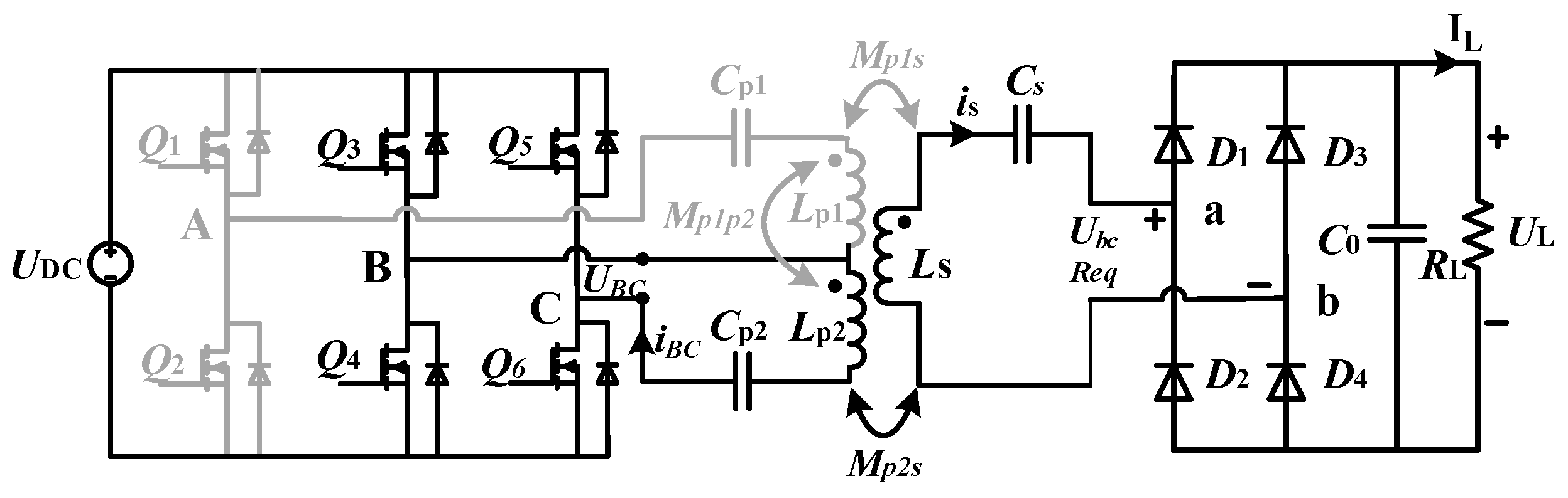
2.1. System Structure
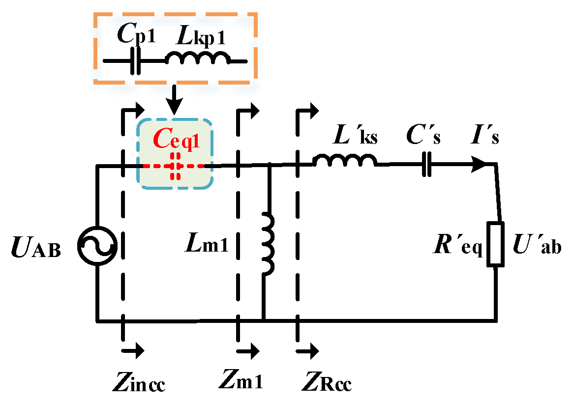
2.2. CC Mode
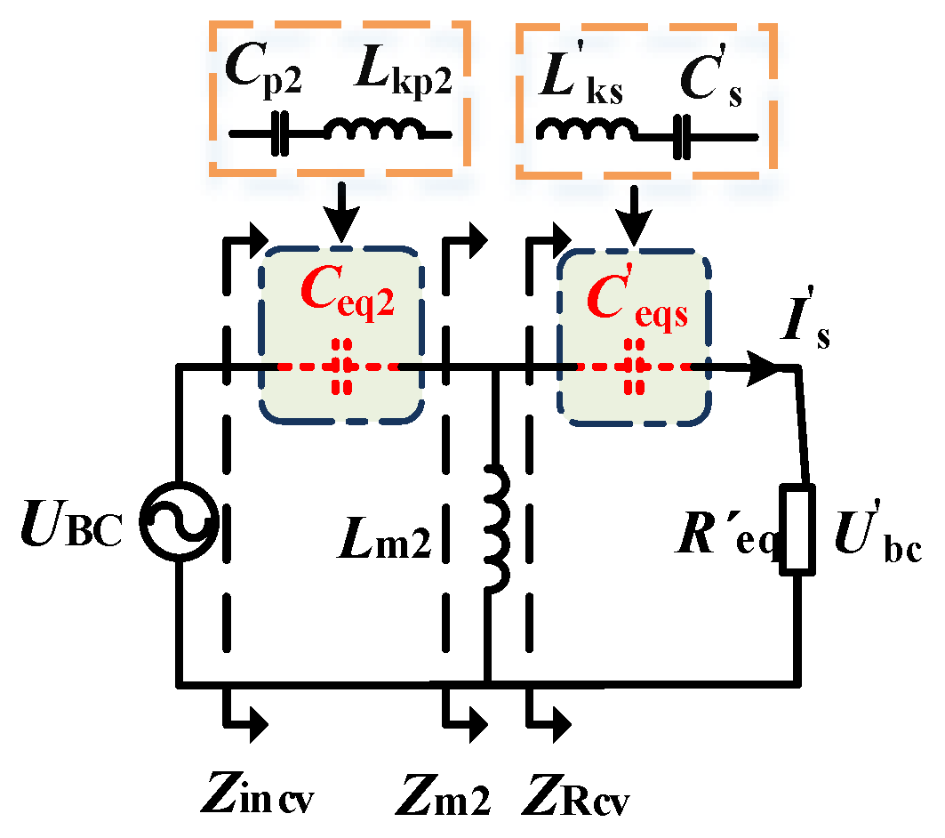
2.3. CV Mode
3. Simulation and Experiment
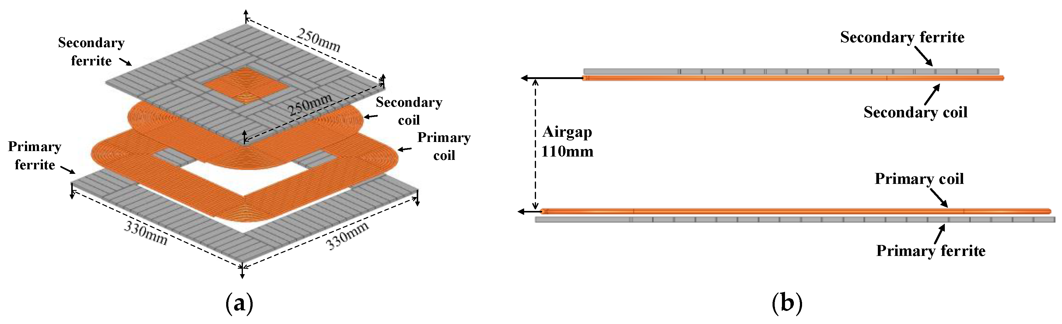
3.1. Parameter Design
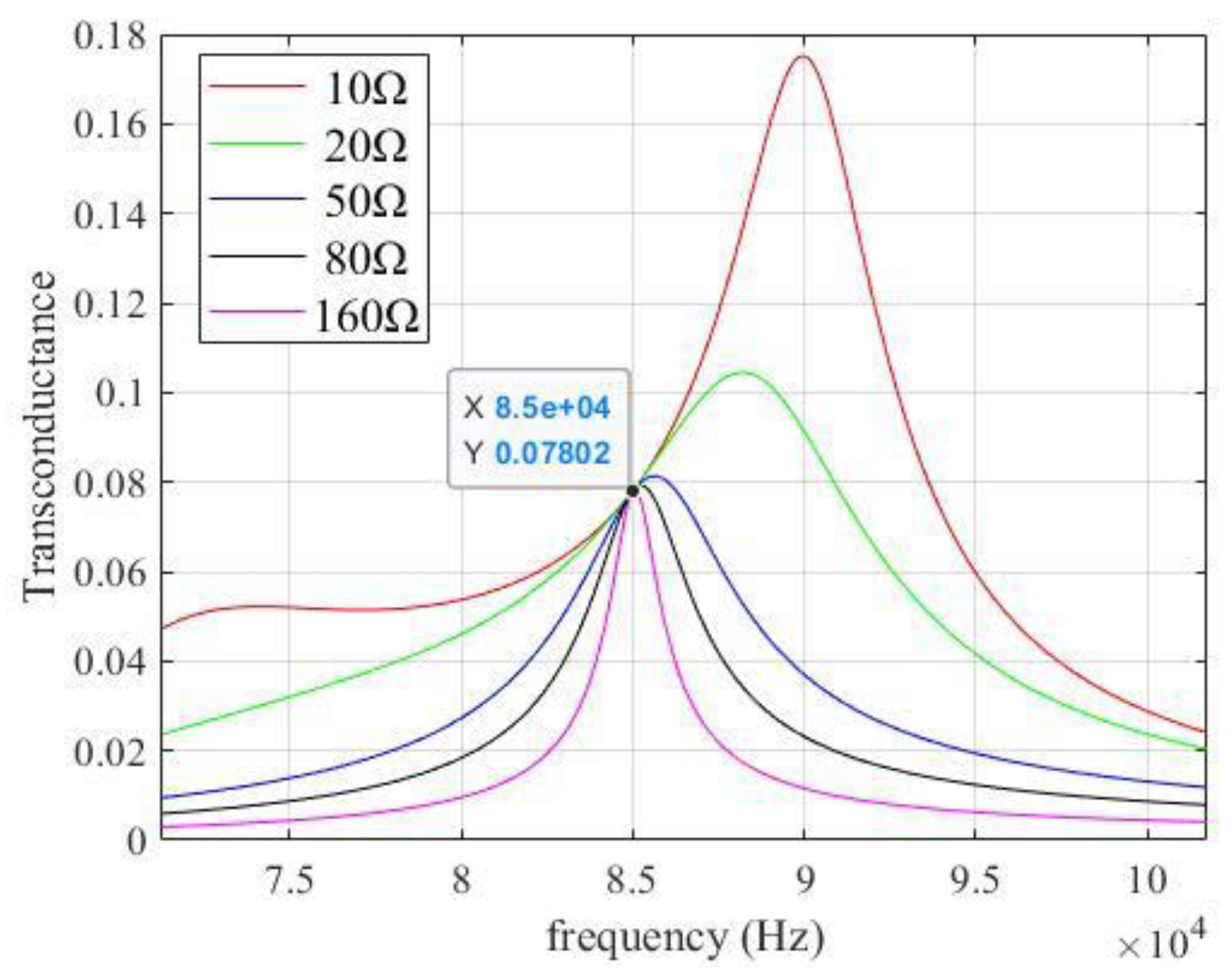
3.2. Simulation Results
3.3. Experimental Results
4. Conclusions
Author Contributions
Funding
Conflicts of Interest
References
- RamRakhyani, A.K.; Mirabbasi, S.; Chiao, M. Design and Optimization of Resonance-Based Efficient Wireless Power Delivery Systems for Biomedical Implants. IEEE Trans. Biomed. Circuits Syst. 2011, 5, 48–63. [Google Scholar] [CrossRef] [PubMed]
- Li, Q.; Liang, Y.C. An Inductive Power Transfer System with a High-Q Resonant Tank for Mobile Device Charging. IEEE Trans. Power Electron. 2015, 30, 6203–6212. [Google Scholar] [CrossRef]
- Beh, H.Z.Z.; Covic, G.A.; Boys, J.T. Investigation of Magnetic Couplers in Bicycle Kickstands for Wireless Charging of Electric Bicycles. IEEE J. Emerg. Sel. Top. Power Electron. 2015, 3, 87–100. [Google Scholar] [CrossRef]
- Zhang, W.; White, J.C.; Abraham, A.M.; Mi, C.C. Loosely Coupled Transformer Structure and Interoperability Study for EV Wireless Charging Systems. IEEE Trans. Power Electron. 2015, 30, 6356–6367. [Google Scholar] [CrossRef]
- Villa, J.L.; Sallan, J.; Osorio, J.F.S.; Llombart, A. High-Misalignment Tolerant Compensation Topology for ICPT Systems. IEEE Trans. Ind. Electron. 2012, 59, 945–951. [Google Scholar] [CrossRef]
- Khaligh, A.; Dusmez, S. Comprehensive Topological Analysis of Conductive and Inductive Charging Solutions for Plug-In Electric Vehicles. IEEE Trans. Veh. Technol. 2012, 61, 3475–3489. [Google Scholar] [CrossRef]
- Sallan, J.; Villa, J.L.; Llombart, A.; Sanz, J.F. Optimal Design of ICPT Systems Applied to Electric Vehicle Battery Charge. IEEE Trans. Ind. Electron. 2009, 56, 2140–2149. [Google Scholar] [CrossRef]
- Gerssen-Gondelach, S.J.; Faaij, A.P.C. Performance of batteries for electric vehicles on short and longer term. J. Power Sour. 2012, 212, 111–129. [Google Scholar] [CrossRef]
- Qu, X.; Han, H.; Wong, S.; Tse, C.K.; Chen, W. Hybrid IPT Topologies With Constant Current or Constant Voltage Output for Battery Charging Applications. IEEE Trans. Power Electron. 2015, 30, 6329–6337. [Google Scholar] [CrossRef]
- Yilmaz, M.; Krein, P.T. Review of Battery Charger Topologies, Charging Power Levels, and Infrastructure for Plug-In Electric and Hybrid Vehicles. IEEE Trans. Power Electron. 2013, 28, 2151–2169. [Google Scholar] [CrossRef]
- Gati, E.; Kampitsis, G.; Manias, S. Variable Frequency Controller for Inductive Power Transfer in Dynamic Conditions. IEEE Trans. Power Electron. 2017, 32, 1684–1696. [Google Scholar] [CrossRef]
- Buja, G.; Bertoluzzo, M.; Mude, K.N. Design and Experimentation of WPT Charger for Electric City Car. IEEE Trans. Ind. Electron. 2015, 62, 7436–7447. [Google Scholar] [CrossRef]
- Lu, J.; Zhu, G.; Shou, Y.; Liu, F. Coupling- and Load-Independents Output Voltage and ZPA Operation in LCC-Series Compensated IPT System. In Proceedings of the 2018 IEEE Energy Conversion Congress and Exposition (ECCE), Portland, OR, USA, 23–27 September 2018; pp. 1172–1176. [Google Scholar]
- Lu, J.; Zhu, G.; Wang, H.; Lu, F.; Jiang, J.; Mi, C.C. Sensitivity Analysis of Inductive Power Transfer Systems With Voltage-Fed Compensation Topologies. IEEE Trans. Veh. Technol. 2019, 68, 4502–4513. [Google Scholar] [CrossRef]
- Rahnamaee, H.R.; Madawala, U.K.; Thrimawithana, D.J. A modified hybrid multi-level converter for high-power high-frequency IPT systems. In Proceedings of the 2014 International Power Electronics and Application Conference and Exposition, Shanghai, China, 5–8 November 2014; pp. 624–629. [Google Scholar]
- Li, Y.; Mai, R.; Lu, L.; He, Z.; Liu, S. Harmonic elimination and power regulation based five-level inverter for supplying IPT systems. In Proceedings of the 2015 IEEE PELS Workshop on Emerging Technologies, Wireless Power (2015 WoW), Daejeon, South Korea, 5–6 June 2015; pp. 1–4. [Google Scholar]
- Cheng, C.; Zhou, Z.; Li, W.; Zhu, C.; Deng, Z.; Mi, C.C. A Multi-Load Wireless Power Transfer System With Series-Parallel-Series Compensation. IEEE Trans. Power Electron. 2019, 34, 7126–7130. [Google Scholar] [CrossRef]
- Liu, F.; Yang, Y.; Ding, Z.; Chen, X.; Kennel, R.M. A Multifrequency Superposition Methodology to Achieve High Efficiency and Targeted Power Distribution for a Multiload MCR WPT System. IEEE Trans. Power Electron. 2018, 33, 9005–9016. [Google Scholar] [CrossRef]
- Lu, J.; Zhu, G.; Lin, D.; Wong, S.; Jiang, J. Load-Independent Voltage and Current Transfer Characteristics of High-Order Resonant Network in IPT System. IEEE J. Emerg. Sel. Top. Power Electron. 2019, 7, 422–436. [Google Scholar] [CrossRef]


| Parameters | Value |
|---|---|
| UDC | 220 V |
| UL | 260 V |
| k | 0.2 |
| The LCT coil inductance (Lp1 = Lp2 = Ls) | 120 µH |
| The resonance frequency fcc/fcv | 85 kHz |
| The system output power (P) | 3.3 kW |
© 2019 by the authors. Licensee MDPI, Basel, Switzerland. This article is an open access article distributed under the terms and conditions of the Creative Commons Attribution (CC BY) license (http://creativecommons.org/licenses/by/4.0/).
Share and Cite
Luo, B.; Shou, Y.; Lu, J.; Li, M.; Deng, X.; Zhu, G. A Three-Bridge IPT System for Different Power Levels Conversion under CC/CV Transmission Mode. Electronics 2019, 8, 884. https://doi.org/10.3390/electronics8080884
Luo B, Shou Y, Lu J, Li M, Deng X, Zhu G. A Three-Bridge IPT System for Different Power Levels Conversion under CC/CV Transmission Mode. Electronics. 2019; 8(8):884. https://doi.org/10.3390/electronics8080884
Chicago/Turabian StyleLuo, Bingyang, Yatao Shou, Jianghua Lu, Ming Li, Xiangtian Deng, and Guorong Zhu. 2019. "A Three-Bridge IPT System for Different Power Levels Conversion under CC/CV Transmission Mode" Electronics 8, no. 8: 884. https://doi.org/10.3390/electronics8080884