1. Introduction
With recent developments in green lighting and energy saving around the world, light-emitting diodes (LEDs) are characterized by their small size, long life, high brightness and environmental friendliness [
1,
2,
3]. As a result, LEDs have begun to play important roles as new solid-state light sources for indoor and outdoor energy-saving applications in our daily lives [
4,
5,
6,
7,
8,
9,
10,
11].
Streetlights that illuminate the road are designed to provide a safe night-time environment for cars, motorcycles, cyclists and pedestrians. The traditional source of illumination for streetlight applications is high-pressure mercury lamps, because of their low installation cost. However, high-pressure mercury lamps consume more energy and save less electricity. In addition, the discharge tubes of these lamps contain mercury vapor, which is harmful and can cause pollution to our environment when the lamp is exhausted. Therefore, LED streetlights with energy-saving features have begun replacing traditional high-pressure mercury street lamps [
12,
13]. Traditional two-stage drivers for LED streetlight applications include AC–DC converters with power-factor correction (PFC) and DC–DC converters that provide rated voltage and current to the LED streetlight [
14,
15]. However, the circuit is not efficient, and requires more power switches and components in a conventional two-stage streetlight driver. The literature presents some single-stage streetlight drivers that integrate an AC–DC converter with a DC–DC converter [
16,
17,
18,
19,
20].
Figure 1 shows an existing single-stage LED streetlight driver, which combines an interleaved boost converter with a half-bridge-type LLC resonant converter into a single-stage power converter for supplying the LED street-lighting module at a utility-line voltage of 110V [
16]. The LED streetlight driver comprises a low-pass filter, a bridge rectifier (
Dr1,
Dr2,
Dr3 and
Dr4), two capacitors (
Cin1 and
Cin2), two diodes (
DB1 and
DB2), two inductors (
L1 and
L2), two power switches (
S1 and
S2), a DC-linked capacitor
CDC, a resonant capacitor
Cr and an inductor
Lr, a center-tapped transformer
T with two output windings, two diodes (
D1 and
D2), a capacitor
Co and the LED streetlight module. This kind of single-stage streetlight driver based on interleaved boost conversion is suitable for operating at utility-line voltages from 100~120 V in American and Asian countries, but will tolerate high voltage levels on the DC-linked capacitor
CDC when it operates at higher utility-line voltages due to boost-type power conversion, such as the 220~240 V in European countries. In addition, the voltage stresses of the power switches in this version will increase. Another existing single-stage LED streetlight driver, which integrates an interleaved boost PFC converter with a half-bridge-type series-resonant converter cascaded with a bridge rectifier for supplying the LED street-lighting module at a utility-line voltage of 220 V was proposed in [
20], and high voltage stresses of power switches occurred in this version due to the boost-type power conversion; therefore, the level of DC-bus voltage is increased, and two DC-linked capacitors are required.
To meet these challenges, this paper proposes and implements a single-stage LED streetlight driver based on interleaved buck-boost conversion with PFC and soft-switching functions, which is suitable for operating at high utility-line voltages along with reduced voltage levels on the DC-linked capacitor and decreased voltage stresses on the power switches due to a buck-boost-type power conversion. This paper introduces the description and analysis of the operating modes, the design considerations of the key circuit components in the proposed LED streetlight driver, and experimental results obtained from the 144 W (36V/4A)-rated prototype circuit are included.
2. Circuit Derivation and Analysis of the Proposed Single-Stage LED Streetlight Driver
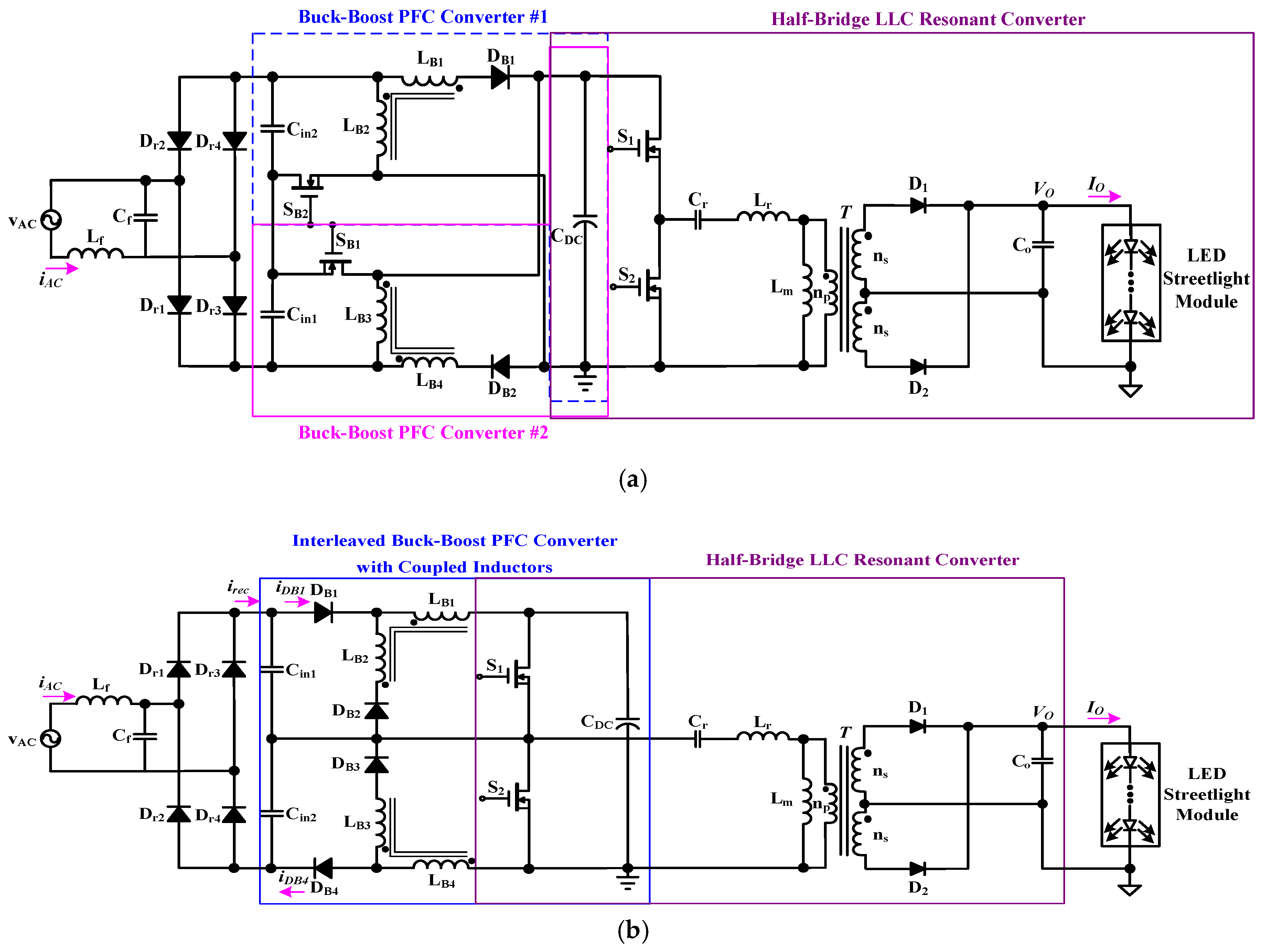
Figure 2a shows the original two-stage LED streetlight driver, which consists of buck-boost PFC converter #1 and buck-boost PFC converter #2 with interleaved operation in series connection with a half-bridge LLC resonant converter. In addition, the two coupled inductors are employed instead of single-winding inductors in order to accomplish buck-boost conversion.
Figure 2b shows the presented LED streetlight driver with soft-switching and interleaved PFC feature, which integrates an interleaved buck-boost PFC converter with a half-bridge LLC resonant converter into single-stage power conversion and includes a low-pass filter (
Lf and
Cf), a bridge rectifier (
Dr1,
Dr2,
Dr3 and
Dr4), two capacitors (
Cin1 and
Cin2), two coupled inductors (
LB1 and
LB2;
LB3 and
LB4), four diodes (
DB1,
DB2,
DB3, and
DB4), two power switches (
S1 and
S2), a DC-bus capacitor (
CDC), a resonant capacitor (
Cr), a resonant inductor (
Lr), a center-tapped transformer
T with a magnetizing inductor
Lm and two output windings, two output diodes
D1 and
D2, an output capacitor (
Co) and the LED streetlight module. In addition, the diodes
DB2 and
DB3 are used to prevent current from entering the inductors
LB2 and
LB3 from the AC mains voltage sources. Furthermore, diodes
DB1 and
DB4 are capable of preventing the inductor currents from returning to the input capacitors
Cin1 and
Cin2. Since the voltage on the capacitor
Cin1 or
Cin2 is half of the utility-line voltage, the DC-bus voltage and the peak current of each coupled inductor will also be half. Due to the reduced DC-bus voltage, power switches with decreased voltage-stress can be utilized in the proposed LED streetlight driver, which is advantageous for high utility-line voltage applications.
Figure 3 shows a simplified circuit of the proposed single-stage LED streetlight driver when analyzing its operating modes. To describe the operation of the proposed LED streetlight driver, the following assumptions are made.
- (a)
Since the switching frequency of the power switches is much higher than the utility-line frequency, the sinusoidal utility-line voltage can be considered to be a constant value in each high-frequency switching period.
- (b)
The voltage sources VREC1 and VREC2 of capacitors Cin1 and Cin2, respectively, represent the rectified input utility-line voltages.
- (c)
The power switches S1 and S2 operate complementarily, and their intrinsic body diode and drain-source capacitance are taken into consideration.
- (d)
The turn-on voltage drops of diodes (DB1, DB2, DB3, DB4, D1 and D2) are omitted.
- (e)
To naturally obtain PFC, the coupled inductors (LB1 and LB2; LB3 and LB4) are designed to operate in discontinuous-conduction mode (DCM).
The operational modes and key waveforms of the LED streetlight driver proposed in this paper are shown in
Figure 4 and
Figure 5, respectively, and the analysis of the operation is described in detail below.
Mode 1 (
t0 ≤
t <
t1; in
Figure 4a): When the switch voltage
vDS1 decreases to zero and the body diode of switch
S1 is forward-biased at time interval
t0, this mode begins and the power switch
S1 turns on with zero-voltage switching (ZVS). The voltage source
VREC1 charges the coupled inductor
LB1 through diode
DB1 and switch
S1. The inductor current
iLB1 increases linearly from zero and can be given by:
where
vAC-rms represents the rms value of input utility-line voltage, and
fAC represents the utility-line frequency.
The resonant inductor Lr and magnetizing inductor Lm provide energy to the resonant capacitor Cr and to DC-linked capacitor CDC through the body diode of switch S1, and to the output capacitor Co and the LED streetlight module through transformer T and output diode D1. The diode DB3 is forward-biased, and the coupled inductors LB3 and LB4 provide energy to the drain-source capacitor of switch S2 through diode DB3. This mode ends when the resonant inductor current iLr is zero at time t1.
Mode 2 (
t1 ≤
t <
t2; in
Figure 4b): This mode is activated when the resonant inductor current
iLr reaches zero at
t1. The voltage source
VREC1 continues charging the coupled inductor
LB1 through diode
DB1 and switch
S1.
The capacitors CDC, the magnetizing inductor Lm and the coupled inductors LB3 and LB4 provide energy to the drain-source capacitor of switch S2, the resonant inductor Lr and the resonant capacitor Cr through DB3, and to the output capacitor Co and the LED streetlight module through transformer T and output diode D1. When the magnetizing inductor current iLm and inductor current iLB4 become zero at t2, this mode finishes.
Mode 3 (
t2 ≤
t <
t3; in
Figure 4c): At
t2, the voltage source
VREC1 continues charging the coupled inductor
LB1 through
DB1 and
S1. The capacitors
CDC provides energy to the resonant inductor
Lr, the resonant capacitor
Cr, and the magnetizing inductor
Lm through
S1, and to the output capacitor
Co and the LED streetlight module through transformer
T and output diode
D1. This mode ends when the diode current
iD1 becomes zero at
t3.
Mode 4 (
t3 ≤
t <
t4; in
Figure 4d): This mode activates when
iD1 is zero at
t3. The voltage source
VREC1 continues charging the coupled inductor
LB1 through
DB1 and
S1. The capacitor
CDC continues providing energy to the inductors
Lr and
Lm and to
Cr through
S1. The output capacitor
Co provides energy to the LED streetlight module. The coupled-inductor current
iLB1 reaches its peak value at
t4, which is denoted as
iLB1-pk(t), and is given by:
where
TS and
D are the period and the duty cycle of the power switch, respectively.
When switch S1 turns off at t4, this mode finishes.
Mode 5 (
t4 ≤
t <
t5; in
Figure 4e): This mode begins when
S1 is off and
iLB1 is at its maximum level at
t4. The diode
DB2 is forward-biased and coupled inductors
LB1 and
LB2 provide energy to the drain-source capacitor of
S1 through
DB2. The coupled-inductor current
iLB1 linearly decreases, and it can be given by:
where
VDC represents the voltage of the DC-bus capacitor.
The capacitor CDC and the drain-source capacitor of S2, provide energy to inductors Lr and Lm and to Cr. The output capacitor Co continues providing energy to the LED streetlight module. At time interval t5, the voltage vDS2 of power switch S2 is decreased to zero; then this mode ends.
Mode 6 (
t5 ≤
t <
t6; in
Figure 4f): When the switch voltage
vDS2 is decreased to zero and the body diode of switch
S2 is forward-biased at
t5, this mode activates and the power switch
S2 turns on with ZVS feature. The voltage source
VREC2 provides energy to coupled inductor
LB4 through diode
DB4 and switch
S2, and the inductor current
iLB4 increases linearly from zero. The coupled inductors
LB1 and
LB2 continue providing energy to the drain-source capacitor of
S1 through
DB2, and the inductor current
iLB1 continues linearly decreasing. The capacitor
CDC continues providing energy to inductors
Lr and
Lm and to the resonant capacitor
Cr through the body diode of
S2. The output capacitor
Co continues providing energy to the LED streetlight module. This mode finishes when the magnetizing inductor current
iLm reaches its peak value at
t6.
Mode 7 (
t6 ≤
t <
t7; in
Figure 4g): This mode begins when the magnetizing inductor current
iLm is at its maximum level at
t6. The voltage source
VREC2 continues providing energy to coupled inductor
LB4 through diode
DB4 and switch
S2, and
iLB4 continues linearly increasing. The coupled inductors
LB1 and
LB2 continue providing energy to the drain-source capacitor of
S1 through
DB2, and
iLB1 continues linearly decreasing. The DC-linked capacitor
CDC provides energy to the drain-source capacitor of
S1 through
S2. The resonant inductor
Lr provides energy to resonant capacitor
Cr through switch
S2. The magnetizing inductor
Lm provides energy to the output capacitor
Co and the LED streetlight module through transformer
T and diode
D2. This mode ends when the inductor current
iLB1 is decreased to zero at
t7.
Mode 8 (
t7 ≤
t <
t8; in
Figure 4h): This mode activates when the current
iLB1 is zero at
t7. The voltage source
VREC2 continues providing energy to coupled inductor
LB4 through diode
DB4 and switch
S2. The coupled inductors
LB1 and
LB2 continue providing energy to the drain-source capacitor of
S1 through
DB2. The DC-linked capacitor
CDC continues providing energy to the drain-source capacitor of
S1 through
S2. The resonant inductor
Lr and the magnetizing inductor
Lm provide energy to resonant capacitor
Cr through switch
S2 and to the output capacitor
Co along with the LED streetlight module through transformer
T and diode
D2. This mode finishes when the magnetizing inductor current
iLm is decreased to zero at
t8.
Mode 9 (
t8 ≤
t <
t9; in
Figure 4i): This mode begins when the magnetizing inductor current
iLm is zero at
t8. The voltage source
VREC2 continues providing energy to coupled inductor
LB4 through diode
DB4 and switch
S2, and
iLB4 continues linearly increasing. The DC-linked capacitor
CDC continues providing energy to the drain-source capacitor of
S1 through
S2. The inductors
Lr and
Lm continue providing energy to the capacitor
Cr through switch
S2, and to the output capacitor
Co along with the LED streetlight module through transformer
T and diode
D2. When the diode current
iD2 decreases to zero, this mode ends.
Mode 10 (
t9 ≤
t <
t10; in
Figure 4j): This mode activates when the current
iD2 is zero at
t9. The voltage source
VREC2 continues providing energy to the coupled inductor
LB4 through
DB4 and
S2, and
iLB4 continues increasing linearly. The DC-linked capacitor
CDC continues providing energy to the drain-source capacitor of
S1 through
S2. The inductors
Lr and
Lm continue providing energy to the capacitor
Cr through switch
S2. The output capacitor
Co supplies energy to the LED streetlight module. When
S2 turns off and
iLB4 reaches its peak value at
t10, this mode finishes.
Mode 11 (
t10 ≤
t <
t11; in
Figure 4k): This mode begins when switch
S2 is turned off and
iLB4 is at its maximum level at
t10. The coupled inductors
LB3 and
LB4 provide energy to the drain-source capacitor of
S2 through
DB3, and the inductor current
iLB4 linearly decreases. The drain-source capacitor of
S1 and the inductors
Lr and
Lm supply energy to capacitors
Cr and
CDC. The output capacitor
Co still provides energy to the LED streetlight module. When the switch voltage
vDS1 decreases to zero at
t11, this mode ends, and
Mode 1 begins again for the next switching period.
4. Experimental Results of the Prototype LED Streetlight Driver
A prototype driver has been successfully developed and implemented for supplying a 144 W-rated (36V/4A) LED streetlight module with an input utility-line voltage of 220 V.
Table 1 and
Table 2, respectively, show the specifications and key components utilized in the presented single-stage LED streetlight driver. Additionally,
Figure 7 shows the proposed LED streetlight driver with control block diagram. A constant-voltage and constant-current (CV-CC) controller is adopted to sense the output voltage through resistors
RVS1 and
RVS2, while simultaneously sensing the output current through the resistor
RCS for supplying the rated voltage and current to the experimental LED street-lighting module. The output signal of the CV-CC controller feeds into the high-voltage resonant controller through a photo-coupler. Two gate-driving signals
vgs1 and
vgs2 generating from the resonant controller regulate the output voltage and current of the LED street-lighting module by utilizing variable-frequency control scheme. Moreover, the coupled-inductors (
LB1,
LB2,
LB3 and
LB4) are designed to be operated at discontinuous conduction mode (DCM) for naturally achieving input-current shaping without utilizing a power-factor-correction controller with a feed-forward controlling path.
The measured waveforms of coupled-inductor currents
iLB1 and
iLB4 are shown in
Figure 8; both have interleaved features and operate in DCM.
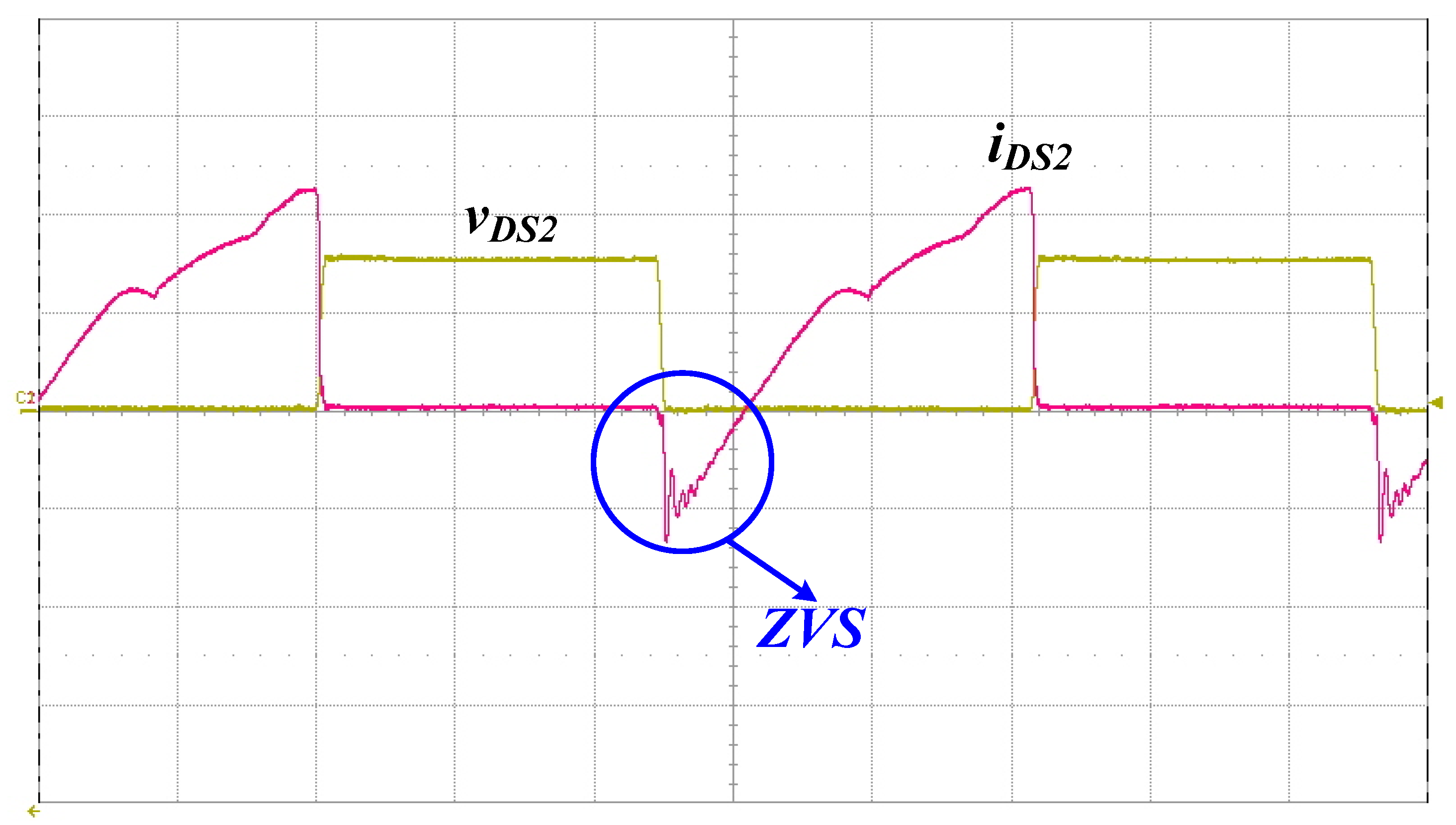
Figure 9 shows the measured switch voltage
vDS2 and switch current
iDS2; thus, ZVS has occurred on the power switch for lowering switching losses.
Figure 10 presents the measured switch voltage
vDS2 and resonant inductor current
iLr.
Figure 11 presents the measured switch voltage
vDS2 and current
iD2 of the output rectified diode
D2; thus, ZCS has occurred on the power diode for decreasing the conduction losses.
Figure 12 depicts the measured output voltage
VO and current
IO; their average values are approximately 36 V and 4 A, respectively.
The measured waveforms of input utility-line voltage
vAC and current
iAC are shown in
Figure 13, and the input current is in phase with utility-line voltage, which results in high power factor. In addition, the measured power factor and the circuit efficiency are 0.9684 and 89.69%, respectively, as measured by a power analyzer (Tektronix PA 4000).
Figure 14 shows the measured input utility-line current harmonics at an input utility-line voltage of 220 V in comparison with the International Electrotechnical Commission (IEC) 61000-3-2 Class C standards; all utility-line current harmonics meet the requirements.
Table 3 shows the measured output voltage ripple and current ripple of the presented LED streetlight driver at a utility-line voltage of 220 V; additionally, the output voltage (current) ripple factor is obtained by the peak-to-peak level divided by the mean value of output voltage (current). It can be seen that the measured voltage and current ripple factors are smaller than 5% and 2%, respectively.
Figure 15 presents a photo of supplying the LED streetlight module with the proposed streetlight driver at an input utility-line voltage of 220V. In addition,
Table 4 shows comparisons between the existing single-stage LED streetlight driver in references [
16,
17,
18,
19] and the one proposed in this paper. According to this table, the proposed single-stage LED streetlight driver has a beneficial feature of reduced voltage stress of power switches, which is favorable for operating with high utility-line voltages, in comparison to the existing single-stage versions in the references [
16,
17,
18,
19]. In addition, the proposed circuit has the lowest current ripple factor among these LED streetlight drivers.

 ,
, 


