Design and Implementation of CPU & FPGA Co-Design Tester for SDN Switches
Abstract
1. Introduction
- To eliminate clock asynchronization, the hardware should be able to process both control plane packets and data plane packets at the same time. Therefore, we combine the control plane and the data plane into a single hardware pipeline and obtain the timestamps for different packets based on the same clock.
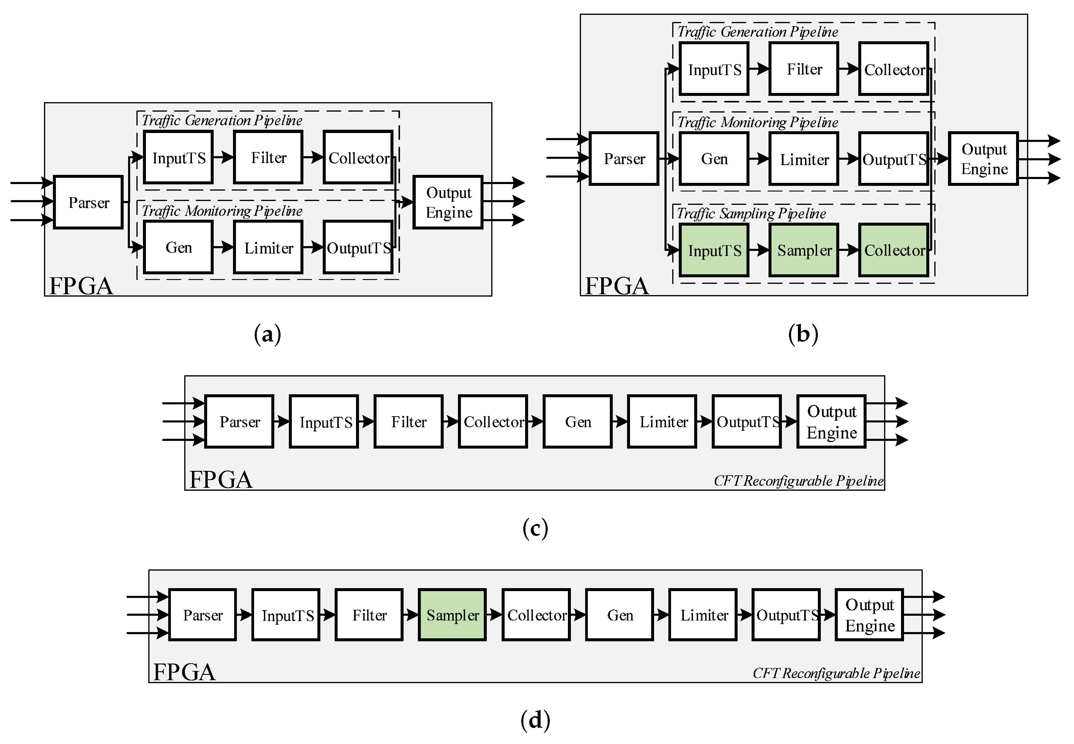
- To provide precise timestamps and specific traffic rates for some particular test scenarios, CFT takes full advantage of the hardware which behaves well in performance and accuracy. CFT uses FPGA as the traffic generation and capture engine and enables the functions of traffic generation and monitoring in a single hardware pipeline, also allows control plane packets to travel through the pipeline. In our pipeline, due to the reuse of hardware function modules, CFT could be able to support more features with as little hardware resources as possible.
- To support more user-defined test cases, CFT takes advantage of the flexibility and scalability of software to provide high-level and user-friendly APIs for users. Through these APIs, the functions supported by the hardware can be called by the software and the corresponding hardware registers or memory locations can be accessed directly. Therefore, users can develop their test cases according to the requirements they need based on the APIs provided by CFT.
- We propose the CFT, a CPU & FPGA co-design Tester, which takes full advantage of hardware and software to enable precise and flexible test for SDN switches.
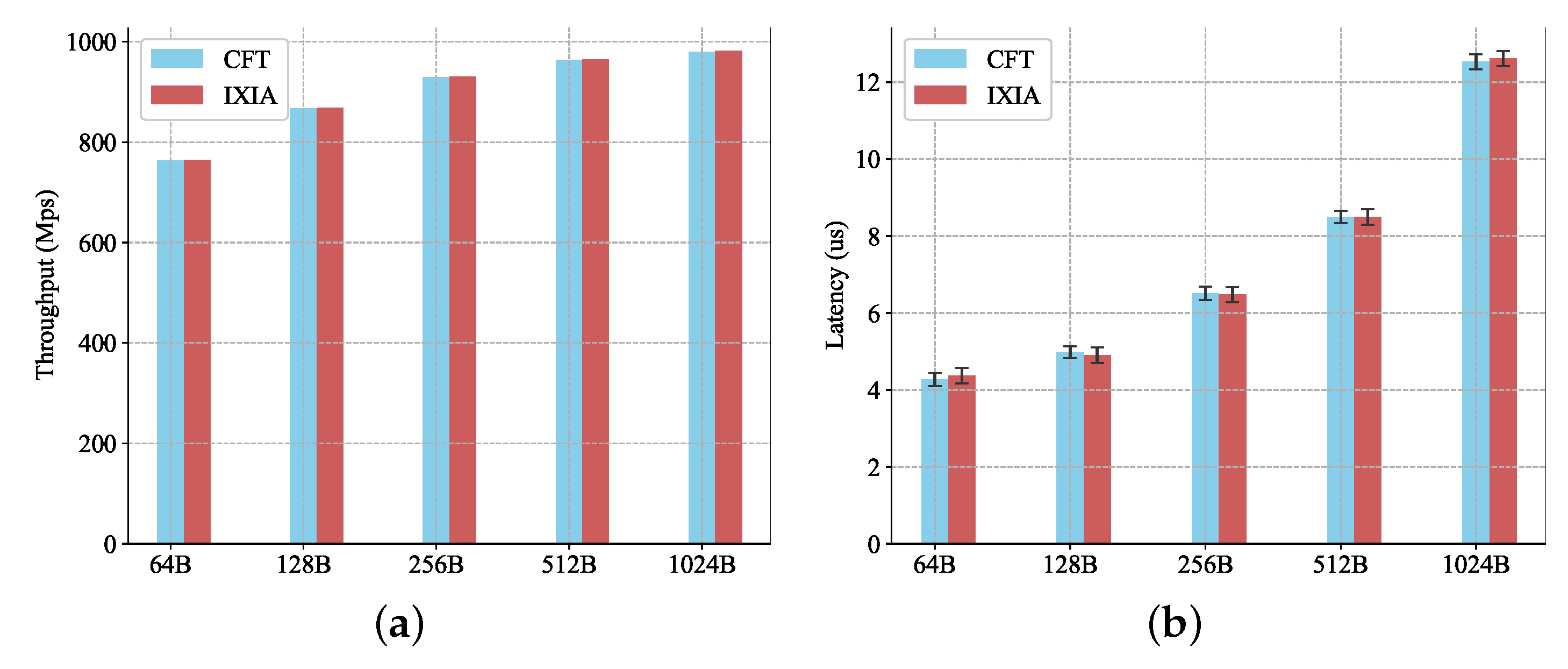
- We solve the problem of clock asynchronization by combining the control plane and the data plane into the same hardware pipeline so that timestamps for different packets are based on the same clock. To ensure normal communication of the control plane, we put forward a scheduling algorithm for arranging the output of control packets and data packets.
- We present a hardware architecture which allows traffic generation and traffic monitoring with high performance and precision in the same pipeline. Due to the reuse of modules and the specifications between modules, users can develop more functions with less consumption of hardware resources.
- We provide specific APIs for users to develop their test cases, which could cover a wide range of test for SDN switches.
2. Overview of CFT for SDN Switches
2.1. Basic Idea of CFT
2.2. The Hardware Design of CFT
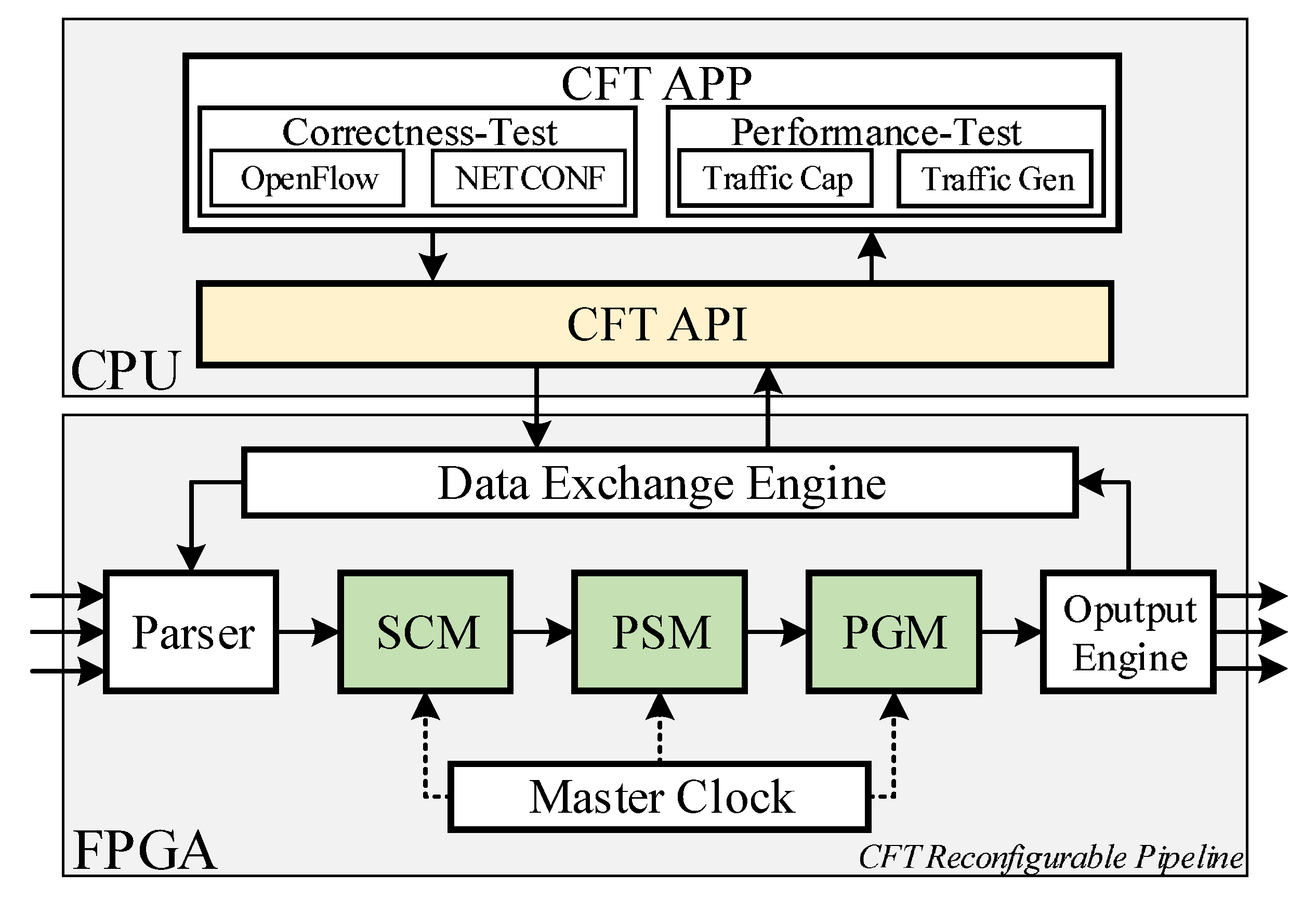
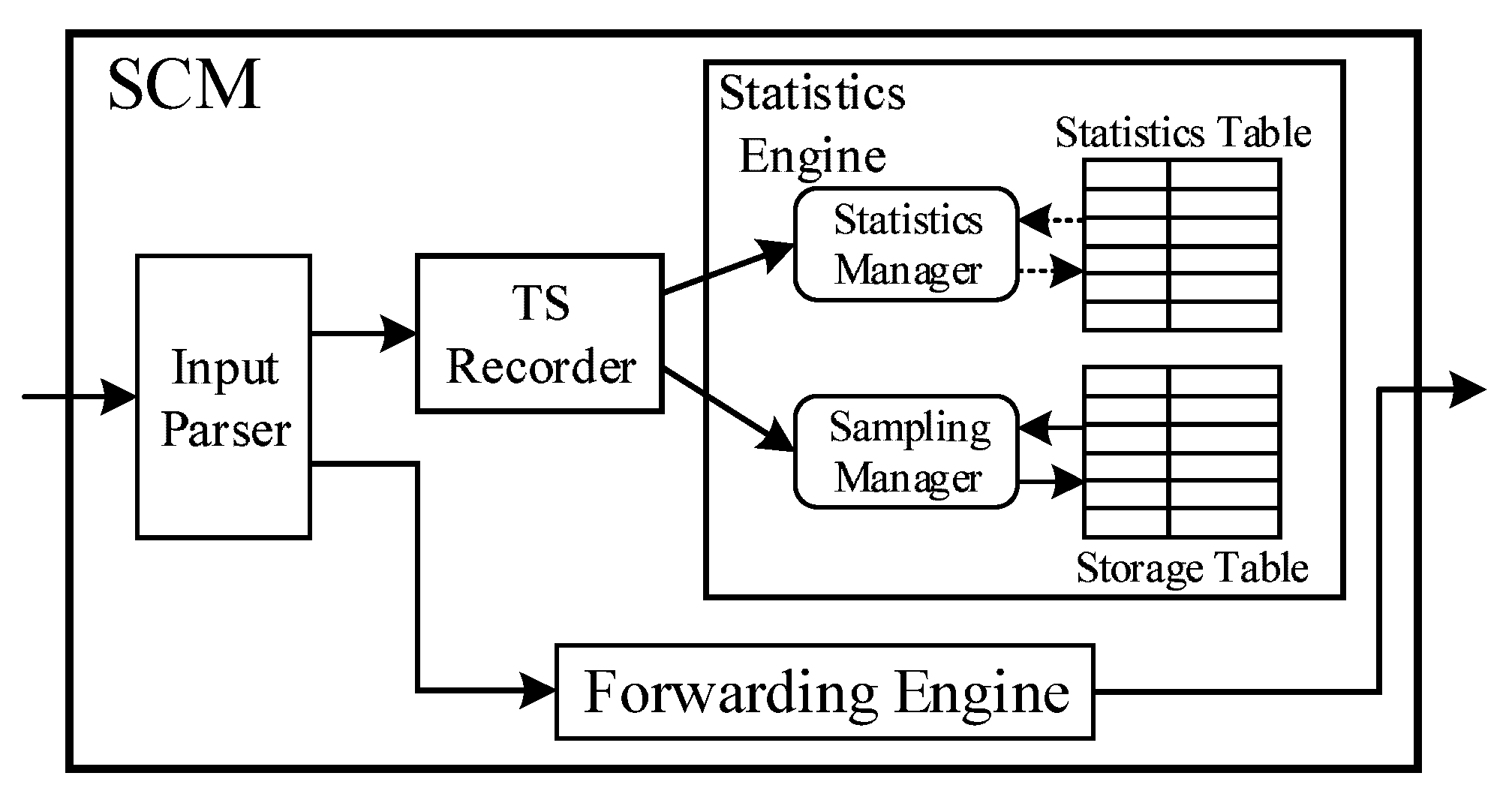
- Statistics Collection Module (SCM). SCM is responsible for recording statistic (total number of bytes, etc.) and sampling specific packets stored into a block RAM. SCM supports the nanosecond-level timestamps for input packets to calculate time-related information, such as forwarding delay.
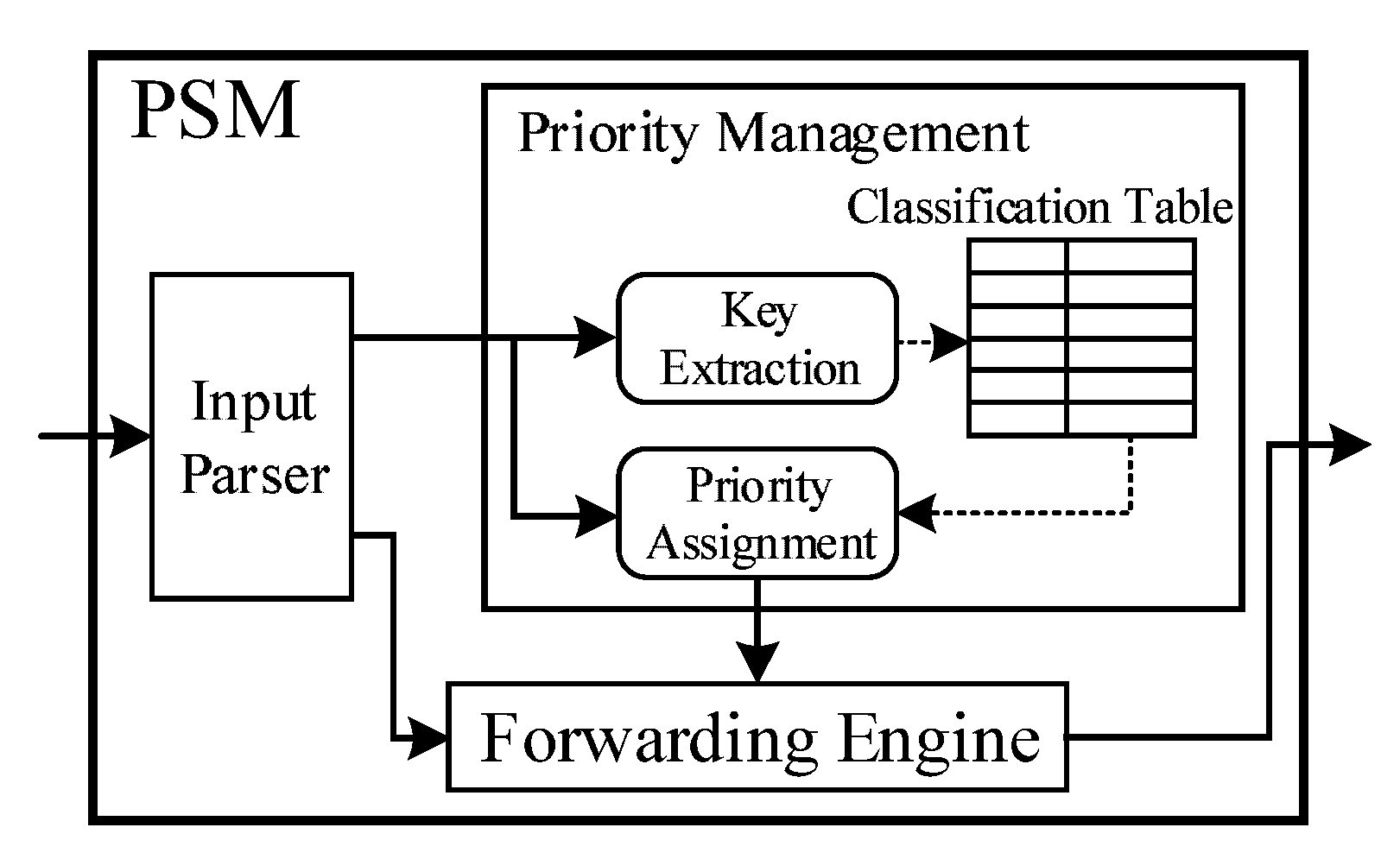
- Packet Schedule Module (PSM). PSM is used to assign priorities for different packets and schedule packets output according to the requirements of test scenarios. We implement a scheduling algorithm in PSM to schedule the output of the control plane packets and the data packets for the correctness of testing.
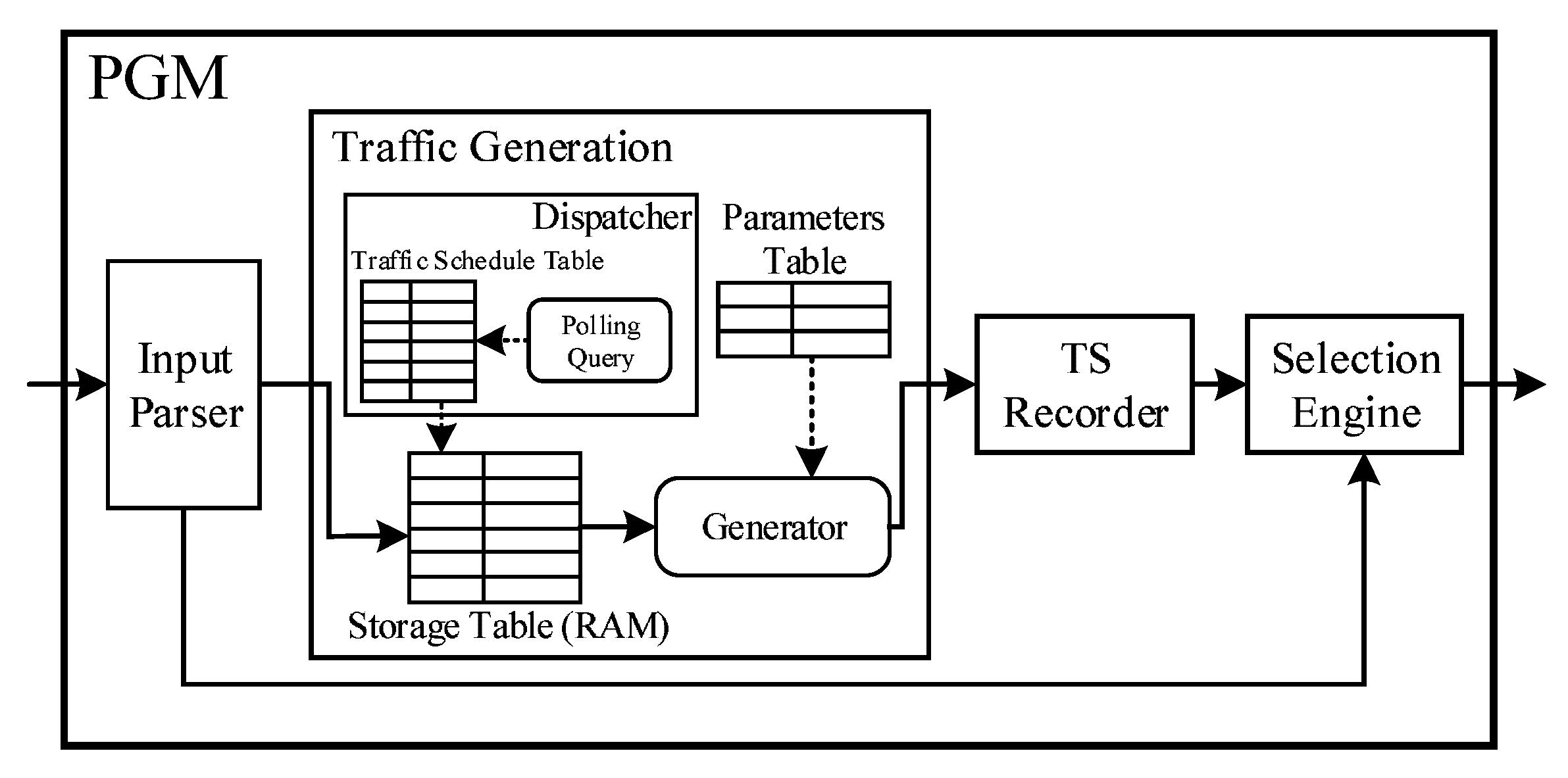
- Packet Generation Module (PGM). PGM is responsible for generating flow according to the pre-defined packet and parameters, including generating rate, time interval and so on. PGM also supports the nanosecond-level timestamps for output packets.
2.3. The Software Design of CFT
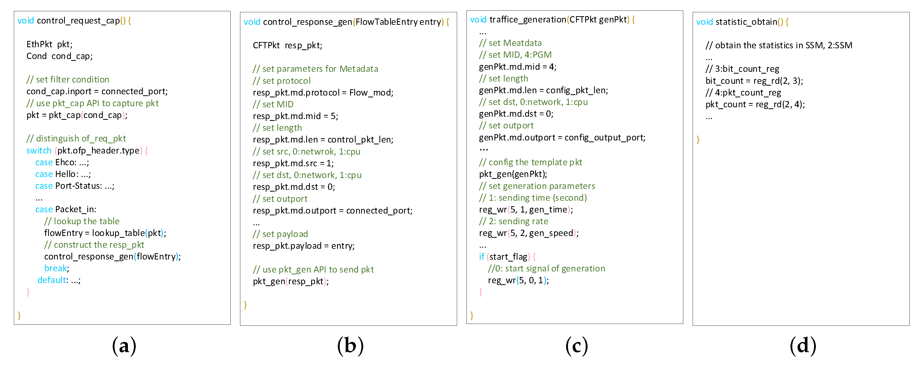
- CFT API Layer. Based on CFT Lib Layer, CFT API Layer abstracts four types of programming interfaces, including pkt_gen, pkt_cap, reg_wr and reg_rd. The first two programming interfaces support the functions of packets generation and packets capture, which is used in traffic generation and monitoring. The latter two programming interfaces are responsible for reading and writing registers to set parameters or obtain statistical data. According to the above APIs provided in CFT API Layer, development of different test cases can be realized, covering various test scenarios for different test purposes. We will discuss more details about APIs in Section 3.
- CFT APP Layer. CFT APP Layer is composed of multiple test cases which are developed based on the APIs provided in CFT API Layer. Users could build their test cases according to the requirements of specific test scenarios. For example, to verify whether the flow table rules are valid, users can construct corresponding packets for different flow table rules and deliver them to verify the validity of flow table rules. Also, users can simulate a controller that supports a specific southbound protocol (e.g., OpenFlow, OF-CONF) to test the protocol correctness of SDN switches with related-protocol.
2.4. The Workflow of CFT
2.4.1. The Performance Test
- (1)
- Configuration Download. When users want to conduct a performance test on SDN switches, template packets should be constructed first. Users can define the type, size and content of packets which are used for traffic generation or to use the packets already provided by the software. At the same time, users should set the parameters of traffic generation, including the sending rate, the sending time, the number of packets sent and the sending port. Parameters will be configured into the FPGA by calling APIs of pkt_gen and reg_wr.
- (2)
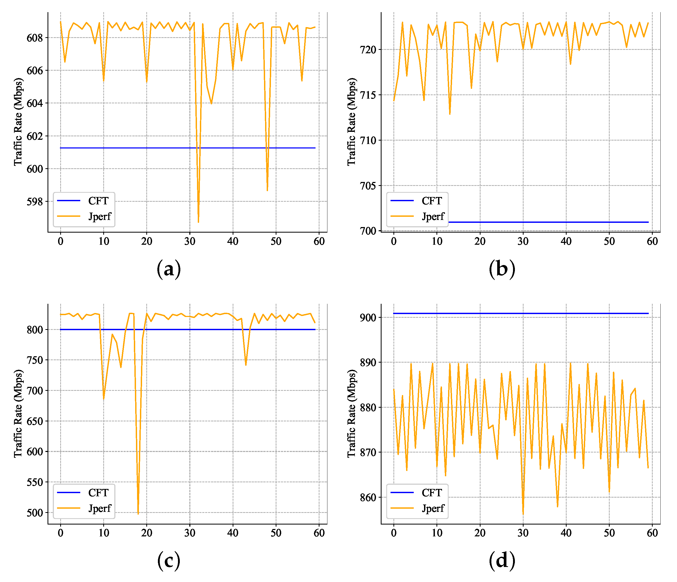
- Traffic Generation. The template packets constructed by users are stored in the block RAMs of the FPGA. Test-related parameters are written into specific hardware registers of the FPGA. When receiving the start signal of traffic generation, the PGM reads packets from the block RAM and send them out continuously according to the parameters. The traffic will be generated at a pre-defined rate and forwarded through the specified port to the tested SDN switch. Each sent packet will be recorded with an output timestamp for further calculating in PGM. When the sending time expires or the number of packets sent is exceeded, traffic generation is terminated.
- (3)
- Traffic Monitoring. When the CFT hardware receives packets from the SDN switch, the SCM will collect the test-related data, such as the number of received packets, bytes of received traffic, and so on. SCM also records an input timestamp for each received packet and will calculate the processing latency (input timestamp minus output timestamp) of the SDN switch. These test-related data will be saved into specific registers which could be obtained by CFT software test cases through CFT APIs we provided. Meanwhile, the SCM will sample some received packets and upload them to software test cases for further analysis.
- (4)
- Statistics Upload. When the test is finished, the CFT software will read the registers and RAMs from the hardware FPGA to obtain the statistic through the APIs of pkt_cap and reg_rd. The software will calculate performance-related test results, such as throughput, processing latency and packet loss rate, based on the statistic. The test results will be presented to users in the form of text and charts.
2.4.2. The Correctness Test
Send Control Packets Actively
- (1)
- Rule Setting. To verify that the tested SDN switch complies with the protocol specification, users will construct the corresponding flow table rules, which are written into the SDN switch. Taking the verification of OpenFlow protocol as an example, users construct the flow_mod messages which contain the rules for the switch.
- (2)
- Rule Writing. The flow_mod messages are forwarded to the tested SDN switch through the port directly connected to the switch management port.
- (3)
- Configuration Download. The CFT needs to generate data plane traffic to verify that the rules in the tested SDN switch are valid. Therefore, users should construct specific packets for generating flow, which can hit the flow table rules. The operations are the same as the performance test.
- (4)
- Traffic Generation. According to the constructed packets and pre-defined parameters, the PGM generates the data plane flow for the tested SDN switch. The operations are the same as the performance test.
- (5)
- Traffic Monitoring. The SCM captures the packets from the specified port of the tested SDN switch and stores them for further analysis.
- (6)
- Rule Verification. The software determines whether the flow table rules written into the tested SDN switch take effect by determining whether packets are captured from the specified switch port (the flow table rules decide) and whether packets are the constructed data plane packets.
Respond Control Packets Passively
- (1)
- Configuration Download. Users need to construct a unique flow that can not be processed by the tested SDN switch, causing request messages (e.g., packet_in messages) from the switch. The operations are the same as the performance test.
- (2)
- Traffic Generation. According to the constructed packets and pre-defined parameters, the PGM generates the data plane flow for the tested SDN switch. The operations are the same as the performance test.
- (3)
- Request Capture. When the tested SDN switch can not process the received flow, it will send request messages to the CFT through the management port. The request messages, acting as control plane packets, will travel through the pipeline and be scheduled by the PSM.
- (4)
- Request Upload. After receiving the packets, the CFT software parses the packets and extract the key fields of the packets.
- (5)
- Response Feedback. According to the key fields of the packets, the CFT software constructs the respond messages like flow_mod or packet_out messages for the tested SDN switches. We will verify whether the response messages from the switch have taken effect by checking the correctness of operations (such as forwarding behavior) on the data plane packets.
3. CFT Design Details
3.1. Statistics Collection Module (SCM)
- (1)
- Input Parser. For each input packet, the Input Parser unit will parse the contents of the packet and extract the key fields of the packet. Based on the information obtained above, the Input Parser unit will determine whether the input packet is a data plane packet or a control plane packet. If the packet is a control plane packet, it will be sent to the Forwarding Engine unit. Otherwise, it will be sent to the next functional unit.
- (2)
- TS Recorder. The TS Recorder unit is responsible for recording an input timestamp for each received data plane packet. The input timestamp will be used to calculate the time-related test items, such as processing latency. After recording the timestamp, the packet will be forwarded to the next functional unit.
- (3)
- Statistics Engine. The Statistics Engine unit consists of registers for saving statistical data and block RAMs for storing sampled packets. When the data plane packet enters, the registers, which store the number of packets, bytes and so on, are updated. Sampled packets are written into the block RAMs according to pre-configured sampling rules. Unsampled packets are discarded after the relevant registers are updated with values.
- (4)
- Forwarding Engine. For control planes packets and software-defined configuration packets, the Forwarding Engine unit forwards these packets directly to the next hardware functional module without any additional operations.
3.2. Packet Schedule Module (PSM)
- (1)
- Input Parser. The Input Parser unit is used to distinguish whether it is a control plane packet or a software-defined configuration packet and forwards them to the corresponding functional units.
- (2)
- Priority Management. The Priority Management unit is responsible for assigning different priority values to different control plane packets by looking up the Classification Table according to the extracted key fields. After assigning priorities, the Priority Management forwards the packets to the Forwarding Engine. At the same time, the Priority Management unit informs the Selection Engine unit in the PGM that the control hardware packets will be output through the hardware pipeline.
- (3)
- Forwarding Engine. The Forwarding Engine unit forwards the software-defined configuration packets and the control plane packets with assigned priorities to the next functional unit.
| Algorithm 1 Priority-based Packets Scheduling (PPS) |
|
3.3. Packet Generation Module (PGM)
- (1)
- Input Parser. The Input Parser unit is used to distinguish whether it is a control plane packet or a software-defined configuration packet. If the packet is a control plane packet, the Input Parser forwards it to the Selection Engine unit. Otherwise, the Input Parser forwards it to the Traffic Generation unit.
- (2)
- Traffic Generation. The Traffic Generation unit is used to continuously send template packets according to the configuration parameters provided by the CFT software, thereby generates the data plane traffic.
- (3)
- TS Recorder. For each output packet, the TS Recorder unit is responsible for recording an output timestamp for the data plane packet, which will be used for further calculation and analysis.
- (4)
- Selection Engine. The Selection Engine is used to determine the output of the control plane packets and the data plane packets based on the priorities and to receive the forwarding signal from the PSM.
| Algorithm 2 Time-based Polling Scheduling (TPS) |
|
| Algorithm 3 Cache-based Packet Ouput (CPO) |
|
3.4. APIs for Test Cases
3.4.1. Operations on Packets
- (1)
- pkt_gen(pkt). Through the API pkt_gen(pkt), users can encapsulate their constructed packets (pkt) into a specific data format which is passed in the hardware pipeline. Packets will be sent after being processed in the pipeline.
- (2)
- pkt_cap(cond). Users can set the conditions (cond) for receiving packets, such as a specific protocol, a specific IP address, a specific input port and so on. The packets captured by calling the library in the CFT Lib Layer are returned to users through the API pkt_cap(cond) after being filtered by cond.
3.4.2. Operations on Registers
- (1)
- reg_wr(MID, wrNum, wrVal). When modifying a register, users should provide the module number (MID), the register number (wrNum) and the value written into the register (wrVal). By calling the API reg_wr, a constructed packet of writing register will be passed to the pipeline and the relevant register will be modified soon.
- (2)
- reg_rd(MID, rdNum). When obtaining the value from the register, users need to provide the module number (MID) and the register number (rdNum). A constructed packet that carries the value will be obtained by calling the library in the CFT Lib Layer and the value will be returned to users through the API reg_rd(MID, rdNum).
3.4.3. API Extension
- (1)
- Users need to develop the format of the packets used for interaction between the CPU and the FPGA;
- (2)
- According to their specific requirements, users develop customized APIs based on the general libraries libnet and libpcap and complie them;
- (3)
- Encapsulate these compiled APIs into the library libcft which contains the CFT APIs we provided. Therefore, different users can use these APIs to develop specific test cases by calling the library libcft.
4. Key Technologies of the Proposed CFT
4.1. CFT Reconfigurable Pipeline
4.2. Key Data Structure in the Pipeline
5. Evaluation
5.1. Precision and Performance
5.2. Protocol Correctness Detection
5.3. Resources Allocation
6. Related Work
7. Conclusions and Future Work
- Abstracting a domain-specific language (DSL) for testing based on the CFT software APIs;
- Extending the testing range of the CFT to the test and verification of SDN controllers and integrated SDN networks.
Author Contributions
Funding
Acknowledgments
Conflicts of Interest
References
- Open Flow Switch Specification 1.5.1. 2019. Available online: https://www.opennetworking.org/wp-content/uploads/2014/10/openflow-switch-v1.5.1.pdf (accessed on 21 July 2019).
- Munjal, A.; Singh, Y.N. An improved autoconfiguration protocol variation by improvising MANETconf. In Proceedings of the 2014 IEEE International Conference on Advanced Networks and Telecommuncations Systems (ANTS), New Delhi, India, 14–17 December 2004; IEEE: Piscataway, NJ, USA, 2014; pp. 1–3. [Google Scholar]
- Kim, H.; Feamster, N. Improving network management with software defined networking. IEEE Commun. Mag. 2013, 51, 114–119. [Google Scholar] [CrossRef]
- Caria, M.; Jukan, A.; Hoffmann, M. A performance study of network migration to SDN-enabled traffic engineering. In Proceedings of the 2013 IEEE Global Communications Conference (GLOBECOM), Atlanta, GA, USA, 9–13 December 2013; IEEE: Piscataway, NJ, USA, 2013; pp. 1391–1396. [Google Scholar]
- Davoli, L.; Veltri, L.; Ventre, P.L.; Siracusano, G.; Salsano, S. Traffic engineering with segment routing: SDN-based architectural design and open source implementation. In Proceedings of the 2015 Fourth European Workshop on Software Defined Networks, Bilbao, Spain, 2 November 2015; IEEE: Piscataway, NJ, USA, 2015; pp. 111–112. [Google Scholar]
- OpenDayLight Organization. 2019. Available online: https://www.opendaylight.org/ (accessed on 21 July 2019).
- Project Floodlight. 2019. Available online: http://www.projectfloodlight.org/ (accessed on 21 July 2019).
- McKeown, N.; Anderson, T.; Balakrishnan, H.; Parulkar, G.; Peterson, L.; Rexford, J.; Shenker, S.; Turner, J. OpenFlow: Enabling innovation in campus networks. ACM SIGCOMM Com. Commun. Rev. 2008, 38, 69–74. [Google Scholar] [CrossRef]
- Rotsos, C.; Sarrar, N.; Uhlig, S.; Sherwood, R.; Moore, A.W. OFLOPS: An open framework for OpenFlow switch evaluation. In Proceedings of the International Conference on Passive and Active Network Measurement, Vienna, Austria, 12–14 March 2012; Springer: Berlin/Heidelberg, Germany, 2012; pp. 85–95. [Google Scholar]
- Rotsos, C.; Antichi, G.; Bruyere, M.; Owezarski, P.; Moore, A.W. OFLOPS-Turbo: Testing the next-generation OpenFlow switch. In Proceedings of the 2015 IEEE International Conference on Communications (ICC), London, UK, 8–12 June 2015; IEEE: Piscataway, NJ, USA, 2015; pp. 5571–5576. [Google Scholar]
- Canini, M.; Venzano, D.; Perešíni, P.; Kostić, D.; Rexford, J. A NICE way to test OpenFlow applications. In Proceedings of the 9th USENIX Symposium on Networked Systems Design and Implementation (NSDI 12), San Jose, CA, USA, 25–27 April 2012; pp. 127–140. [Google Scholar]
- Kuzniar, M.; Peresini, P.; Canini, M.; Venzano, D.; Kostic, D. A SOFT way for openflow switch interoperability testing. In Proceedings of the ACM CoNEXT 2012 the 8th International Conference on Emerging Networking Experiments and Technologies, Nice, France, 10–13 December 2012; pp. 265–276. [Google Scholar]
- Kuzniar, M.; Peresini, P.; Kostic, D. What you Need to Know About SDN Control and Data Planes; Technical Report; EPFL: Lausanne, Switzerland, 2014. [Google Scholar]
- Handigol, N.; Heller, B.; Jeyakumar, V.; Maziéres, D.; McKeown, N. Where is the debugger for my software-defined network? In Proceedings of the First Workshop on Hot Topics in Software Defined Networks, Helsinki, Finland, 13 August 2012; ACM: New York, NY, USA, 2012; pp. 55–60. [Google Scholar]
- Blenk, A.; Basta, A.; Henkel, L.; Zerwas, J.; Kellerer, W.; Schmid, S. perfbench: A tool for predictability analysis in multi-tenant software-defined networks. In Proceedings of the ACM SIGCOMM 2018 Conference on Posters and Demos, Budapest, Hungary, 20–25 August 2018; ACM: New York, NY, USA, 2018; pp. 66–68. [Google Scholar]
- Kuzniar, M.; Canini, M.; Kostic, D. OFTEN testing OpenFlow networks. In Proceedings of the 1st European Workshop on Software Defined Networks (EWSDN 2012), Darmstadt, Germany, 25–26 October 2012. [Google Scholar]
- Monsanto, C.; Reich, J.; Foster, N.; Rexford, J.; Walker, D. Composing software defined networks. In Proceedings of the 10th USENIX Symposium on Networked Systems Design and Implementation (NSDI 13), Lombard, IL, USA, 2–5 April 2013; USENIX: Berkeley, CA, USA, 2013; pp. 1–13. [Google Scholar]
- OFtest. 2019. Available online: http://www.projectfloodlight.org/oftest/ (accessed on 23 July 2019).
- Antichi, G.; Shahbaz, M.; Geng, Y.; Zilberman, N.; Covington, A.; Bruyere, M.; McKeown, N.; Feamster, N.; Felderman, B.; Blott, M.; et al. OSNT: Open source network tester. IEEE Netw. 2014, 28, 6–12. [Google Scholar] [CrossRef]
- Gu, X. Hardware-Based Network Monitoring with Programmable Switch. Senior Thesis, University of Illinois, Urbana, IL, USA, May 2019. [Google Scholar]
- Li, J.; Yang, X.; Sun, Z. DrawerPipe: A reconfigurable packet processing pipeline for FPGA. J. Comput. Res. Dev. 2018, 55, 717–728. [Google Scholar]
- Xilinx Zynq 7000 SoC. 2019. Available online: https://www.xilinx.com/products/silicon-devices/soc/zynq-7000.html (accessed on 18 June 2019).
- Ixia Makes Networks Stronger. 2019. Available online: https://www.ixiacom.com/ (accessed on 23 June 2019).
- Pica8. 2019. Available online: https://www.pica8.com/product/ (accessed on 23 June 2019).
- iPerf—The ultimate speed test tool for TCP, UDP and SCTP. 2019. Available online: https://iperf.fr/ (accessed on 15 July 2019).
- Yang, X.; Sun, Z.; Li, J.; Yan, J.; Li, T.; Quan, W.; Xu, D.; Antichi, G. FAST: Enabling fast software/hardware prototype for network experimentation. In Proceedings of the International Symposium on Quality of Service, Phoenix, AZ, USA, 24–25 June 2019; ACM: New York, NY, USA, 2019. Article No. 32. [Google Scholar]
- NetFPGA. 2019. Available online: https://netfpga.org/ (accessed on 10 June 2019).
- OFSuite_Performance. 2019. Available online: https://www.sdnctc.com/index.php/test_identify/test_identify/id/47 (accessed on 23 July 2019).
- Jarschel, M.; Metter, C.; Zinner, T.; Gebert, S.; Tran-Gia, P. OFCProbe: A platform-independent tool for OpenFlow controller analysis. In Proceedings of the 2014 IEEE Fifth International Conference on Communications and Electronics (ICCE), Danang, Vietnam, 30 July–1 August 2014; IEEE: Piscataway, NJ, USA, 2014; pp. 182–187. [Google Scholar]
- Emmerich, P.; Pudelko, M.; Gallenmüller, S.; Carle, G. FlowScope: Efficient packet capture and storage in 100 Gbit/s networks. In Proceedings of the 2017 IFIP Networking Conference (IFIP Networking) and Workshops, Stockholm, Sweden, 12–16 June 2017; IEEE: Piscataway, NJ, USA, 2017; pp. 1–9. [Google Scholar]
- Zeng, H.; Kazemian, P.; Varghese, G.; McKeown, N. Automatic test packet generation. In Proceedings of the 8th International Conference on Emerging Networking Experiments and Technologies, Nice, France, 10–13 December 2012; ACM: New York, NY, USA, 2012; pp. 241–252. [Google Scholar]
- Spirent—Network, Devices & Services Testing. 2019. Available online: https://www.broadcom.com/ (accessed on 23 June 2019).
- BROADCOM. 2019. Available online: https://www.broadcom.com/ (accessed on 23 June 2019).
- Foerster, K.T.; Schmid, S.; Vissicchio, S. Survey of consistent software-defined network updates. IEEE Commun. Surv. Tutor. 2018, 21, 1435–1461. [Google Scholar] [CrossRef]
- Zhou, W.; Jin, D.; Croft, J.; Caesar, M.; Godfrey, P.B. Enforcing customizable consistency properties in software-defined networks. In Proceedings of the 12th USENIX Symposium on Networked Systems Design and Implementation (NSDI 15), Oakland, CA, USA, 4–6 May 2015; pp. 73–85. [Google Scholar]



| Message | Description | Priority | Remark |
|---|---|---|---|
| Modify_state | Controller manages the flow entries and port status of switch. | 4 | Reject Any Delay |
| Send_packet | Controller specifies the port on the switch that sends packets. | ||
| Barrier | Confirm receipt of packets or completion of operations. | ||
| Packet_in | Request controller to process packets. | ||
| Flow_removed | Tell controller that flow entries have been deleted. | ||
| Port_status | Tell controller that switch port has changed. | ||
| Error | Tell controller that switch has failed. | ||
| Hello | Used to initiate connection establishment between switch and controller. | 3 | Accept Appropriate Delay |
| Echo | Negotiate parameters and confirm alive. | ||
| Features | Controller asks for functions supported by switch. | 2 | Insensitive to Delay |
| Configuration | Set or query configuration parameters of switch. | ||
| Read_state | Query statistics on switch. | ||
| Vendor | Functions defined by vendors. | 1 | Determined by Vendors |
| Initial Transmission Time (T) | Transmission Interval () | Address in RAM () |
|---|---|---|
| ⋯ | ⋯ | ⋯ |
| LUTs | Registers | Block RAM | |
|---|---|---|---|
| SCM | 616 (8.86%,1.16%) | 601 (6.35%,0.56%) | 1 (3.70%,0.71%) |
| PGM | 2624 (37.76%,4.93%) | 1553 (16.42%,1.46%) | 6 (22.22%,4.29%) |
| CFT Pipeline | 6949 (/,13.06%) | 9459 (/,8.89%) | 27 (/,19.29%) |
| Total Resources | 53200 (/,/) | 106400 (/,/) | 140 (/,/) |
| LUTs | Registers | Block RAM | |
|---|---|---|---|
| CFT Pipeline | 13.06% | 8.89% | 19.29% |
| FAST Pipeline | 6.80% | 6.49% | 13.57% |
| Increase | 6.26 % | 2.4% | 5.72% |
© 2019 by the authors. Licensee MDPI, Basel, Switzerland. This article is an open access article distributed under the terms and conditions of the Creative Commons Attribution (CC BY) license (http://creativecommons.org/licenses/by/4.0/).
Share and Cite
Jiang, Y.; Chen, H.; Yang, X.; Sun, Z.; Quan, W. Design and Implementation of CPU & FPGA Co-Design Tester for SDN Switches. Electronics 2019, 8, 950. https://doi.org/10.3390/electronics8090950
Jiang Y, Chen H, Yang X, Sun Z, Quan W. Design and Implementation of CPU & FPGA Co-Design Tester for SDN Switches. Electronics. 2019; 8(9):950. https://doi.org/10.3390/electronics8090950
Chicago/Turabian StyleJiang, Yue, Hongyi Chen, Xiangrui Yang, Zhigang Sun, and Wei Quan. 2019. "Design and Implementation of CPU & FPGA Co-Design Tester for SDN Switches" Electronics 8, no. 9: 950. https://doi.org/10.3390/electronics8090950
APA StyleJiang, Y., Chen, H., Yang, X., Sun, Z., & Quan, W. (2019). Design and Implementation of CPU & FPGA Co-Design Tester for SDN Switches. Electronics, 8(9), 950. https://doi.org/10.3390/electronics8090950


