Article

A Novel 3D Encapsulation Structure Based on Subwavelength Structure and Inserted Pyrex Glass for RF MEMS Infrared Detectors

1
School of Information Science and Technology, Nantong University, Nantong 226019, China
2
School of Electrical Engineering, Nantong University, Nantong 226019, China
3
Tongke School of Microelectronics, Nantong University, Nantong 226019, China
*
Author to whom correspondence should be addressed.
Electronics 2019, 8(9), 974; https://doi.org/10.3390/electronics8090974
Submission received: 24 July 2019 / Revised: 21 August 2019 / Accepted: 30 August 2019 / Published: 31 August 2019
(This article belongs to the Section Microelectronics)

Abstract

:
A novel wafer-level three-dimensional (3D) encapsulation structure was designed for radio-frequency microelectromechanical system (RF MEMS) infrared detectors and investigated by using the finite element method (FEM) simulation. A subwavelength structure with a circular array of coaxial apertures was designed to obtain an extraordinary optical transmission (EOT) on top of a silicon substrate. For perpendicular incident light, a maximum transmission of 56% can be achieved in the long-wave infrared (LWIR) region and the transmission bandwidth covered almost the full LWIR region. Moreover, the maximum transmission could be further promoted with an increase in the incident angle. The vertical silicon vias, insulated by inserted Pyrex glass, were used to generate electrical contacts. With the optimized structure parameters, a feed-through level lower than −82 dB, and a transmission coefficient of one single via of more than −0.032 dB were obtained at a frequency from 0 to 2 GHz, which contributed to the low-loss transmission of the RF signals. Due to the matched thermal expansion coefficients (TECs) between silicon and Pyrex glass, the proposed via structure has excellent thermal reliability. Moreover, its thermal stress is much less than that of a conventional through-silicon via (TSV) structure. These calculated results demonstrate that the proposed 3D encapsulation structure shows enormous potential in RF MEMS infrared detector applications.

1. Introduction

In recent years, uncooled radio-frequency microelectromechanical system (RF MEMS) infrared detectors, based on aluminum nitride (AlN) piezoelectric resonators, are attracting increased attention due to their small size, high performance, high thermo-mechanical coupling, high resolution, and complementary metal-oxide-semiconductor (CMOS) compatible process [1,2]. Unlike photon detectors, RF MEMS infrared detectors can work at room temperature and do not need cryogenic cooling [3,4]. When external perturbations are absorbed by the detectors, their temperature will rise and then the detectors will yield measurable frequency shifts of AlN resonant modes [5]. Frequency shift is a physical quantity that can be monitored with high precision and converted to digital form by simply measuring the zero crossings [1]. However, RF MEMS infrared detectors put forward a higher demand for encapsulation, which is the major concern regarding their commercialization. Several factors such as optical transmission, electrical interconnection, thermal stress, and vacuum sealing materials should be considered in particular to maintain their high performance after packaging.
Wafer-level three-dimensional (3D) packaging is a promising technique for RF MEMS infrared detectors since it has advantages of smaller size and lower power consumption when compared to planar interconnect packaging [6,7,8,9,10,11]. There are two primary types of wafer-level 3D packaging. One is film encapsulation, which utilizes an epitaxial highly doped silicon film to seal devices and vertical silicon feedthroughs to transmit electrical signals [6,7]. Although the film encapsulation can contribute to the miniaturization of devices, its micro-fabrication process is very complicated. Another type is typically based on through-silicon vias (TSVs) and wafer-level bonding [8,9,10,11]. This technique utilizes TSVs to make vertical interconnections, which embed the vertical metal feedthroughs and SiO2 films in bulk silicon to transmit electrical signals and act as the insulation, respectively. However, this technique has some shortcomings including mismatched thermal expansion coefficients (TECs) between the metal and silicon, large dielectric loss, insulation failure, a complex process, and high cost [9]. In addition, the wafer-level bonding between the cap and device wafers is critical to achieve long-term operation as well as high thermal insulation for RF MEMS infrared detectors. The common bonding methods such as Cu–Sn bonding and Au–Sn bonding [11,12] are not cost-effective and easily cause large residue stress in the systems. The silicon wafer with inserted Pyrex glass is a promising 3D packaging structure, which utilizes vertical silicon feedthroughs to transmit electrical signals [13,14,15]. The inserted Pyrex glass acts as the electrical insulation and the anodic bonding material, which also has a matched TEC with silicon. Compared to the above-mentioned 3D packaging structure based on TSVs, the 3D packaging structure with silicon feedthroughs has many outstanding advantages such as lower cost, higher reliability, and a simpler fabrication process. However, its electrical transmission and thermal stress need to be studied systemically for the applications of RF MEMS infrared detectors.
High long-wave infrared (LWIR) absorption is necessary for RF MEMS infrared detectors, which contributes to the detectors being capable of detecting weak signals and a high detection accuracy [1,2,16]. For the encapsulation of RF MEMS infrared detectors, an appropriate infrared transmission with a high optical transmission and optical filtering at the LWIR region is highly desirable to improve LWIR absorption and avoid interferences from other IR regions. A typical packaging cap for infrared detectors uses an antireflection coating as an infrared window, which can reach the maximum transmission of 50%~60% [17,18]. However, its transmission bandwidth is much broader than the needed wavelength range, so it is more difficult to achieve excellent optical filter properties. Integrating plasmon metasurfaces on the packaging cap is an effective method to solve this problem [19]. Metasurfaces with extraordinary optical transmission (EOT) can be synthesized by applying plasmon resonances sustained by subwavelength aperture structures [20,21,22,23]. A silicon substrate with a subwavelength array of apertures can be effectively coupled with the incident light at resonance frequencies, which is beneficial to high optical transmission as well as narrowing the transmission bandwidth [24]. Moreover, the transmission spectra of the subwavelength array can also be easily controlled by adjusting the geometrical parameters of the aperture structure.
This work presents a novel wafer-level 3D encapsulation structure for RF MEMS infrared detectors that utilizes silicon feedthroughs to transmit electrical signals by inserting Pyrex glass as the electrical insulation and the anodic bonding material. The plasmon metasurfaces are used to achieve EOT as well as excellent optical filter properties. The optical transmission, RF electrical transmission, and thermal stress were systematically studied by theoretical analysis as well as by using the finite element method (FEM) simulation.

2. Structure Design and Discussion

In this work, a novel 3D packaging structure was designed for RF MEMS infrared detectors, as shown in Figure 1. Low-resistance silicon feedthroughs, consisting of the input and output ports (I/O ports), were designed to transmit the signals of the detectors with Pyrex glass acting as the insulation between the feedthroughs and the silicon substrate. Furthermore, a bonding ring made of Pyrex glass was designed in the packaging cap, which can be micro-fabricated together with vertical silicon vias by the glass reflow process [13,14,15]. The designed cap wafer can be wafer-level vacuum bonded to a device wafer through the anodic bonding between the Pyrex glass and silicon, without the need for additional solder [25]. An array of subwavelength circular-coaxial apertures in a gold film was designed on top of a silicon substrate in order to enhance optical transmission that produces optical filtering capabilities at the LWIR region. As shown in Figure 1b, a cavity was also designed below the subwavelength structures to accommodate the infrared detector.

2.1. Optical Transmission of the 3D Encapsulation Structure

The proposed 3D packaging cap was systematically studied to optimize its optical transmission by using COMSOL Multiphysics V4.3a software (V4.3a, COMSOL Inc., Stockholm, Sweden). A full width at half maximum (FWHM) at the LWIR region was analyzed, which is an important indicator of the transmission bandwidth. The incident angle was perpendicular to the cap surface in order to study the basic infrared transmission performance. The optical simulation model was one unit cell of the subwavelength aperture structure, which consisted of an air box, a subwavelength aperture, a silicon substrate, two groups of periodic conditions, and incident and transmitted ports, as shown in Figure 2. The air box was set to model the light incident from air to the subwavelength aperture, and the complex refractive index of air was set as 1 + i0. The incident and transmitted ports were set at the top and bottom boundaries of the model, respectively, which were used to model the optical transmission. The four sides of the model were set as two groups of nonadjacent periodic conditions to define the periodicity. The optical performances were calculated in transverse magnetic (TM) mode.
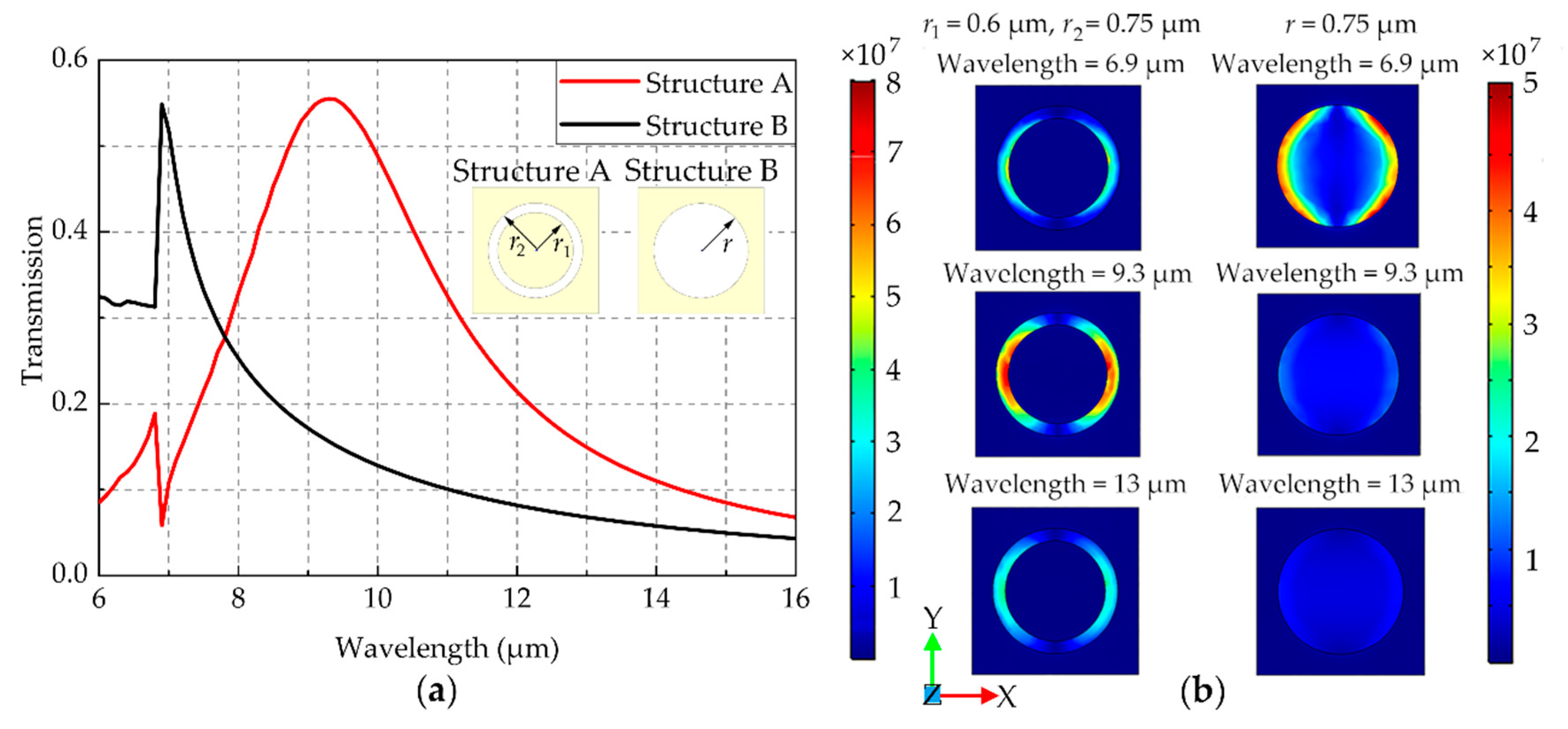
There are two typical subwavelength structures to achieve EOT including the structure with coaxial apertures [26], and the structure with holes [27], designed as shown in Figure 3a. The radius r1 and r2 of the circular-coaxial apertures in Structure A were set as 0.6 μm and 0.75 μm, respectively, and the radius r in Structure B was set as 0.75 μm. The periods of the two structures were all 2 μm. The thicknesses of the gold and silicon were fixed at 90 nm and 100 μm, respectively, which have less effect on the transmission. Gold is known to show negative real and small positive imaginary dielectric constants, which is capable of supporting a surface plasmon resonance (SPR). The complex dielectric constant ε of the gold is defined as below [28]:
ε = ε 1 + i ε 2
where ε1 and ε2 are the real and imaginary parts of the complex dielectric constant ε, respectively. The values of ε1 and ε2 are dependent on the wavenumber, as referred to in [28].
For the optical simulations, the complex refractive index N of the gold can be derived by [29]:
2 n 2 = + ε 1 + [ ε 1 2 + ε 2 2 ] 1 / 2
2 k 2 = ε 1 + [ ε 1 2 + ε 2 2 ] 1 / 2
where n and k are the real and imaginary parts of the complex refractive index N, respectively.
The SPR, supported by the gold, is a coherent oscillation of the surface conduction electrons excited by incident light [30,31,32]. The incident light cannot directly excite the SPR at a smooth gold surface, but the gold film with apertures can contribute to exciting the SPR and enhancing the infrared transmission. For an array of apertures at normal incidence, the peak position λmax excited by the SPR is given approximately by [33,34]:
λ m a x = P i 1 2 + j 1 2 ε 1 ε a i r ε 1 + ε a i r
where P is the array period; i1 and j1 are the scattering orders from the array; and εair is the dielectric constant of air. For both Structures A and B, all parameters were the same in Equation (4). Therefore, in theory, the two structures should have the same peak positions induced by the SPR.
The transmission spectra of Structures A and B are compared in Figure 3a. The transmission peak of Structure B was located at 6.9 μm, which was caused by the SPR. For Structure A, there were two transmission peaks. One peak was associated with the SPR at 6.9 μm, and the other were associated with localized surface plasmon resonance (LSPR) at 9.3 μm. LSPR is a plasmon that oscillates locally around the nanoparticle with a resonance frequency, which can contribute a significant electric-field enhancement. Figure 3b shows the electric-field distribution maps of Structure A and Structure B at the transmission peaks. Both Structure A and Structure B exhibited a transmission peak induced by the SPR at 6.9 μm, based on the periodicity of the array and the same periods of the two structures. This calculated result was well consistent with the theoretical analysis. As shown in Figure 3b, when the incident wavelength was 9.3 μm, Structure A with the circular-coaxial apertures induced a larger electric-field enhancement, while Structure B with the simple hole array could hardly excite the electric-field enhancement. This resulted in a much higher transmission of Structure A around 9.3 μm than that of Structure B. By further increasing the infrared wavelength, the electric-field enhancements of the two structures became weaker. Therefore, the transmission property of Structure A was significantly better than that of Structure B, which is a benefit from the LSPR.
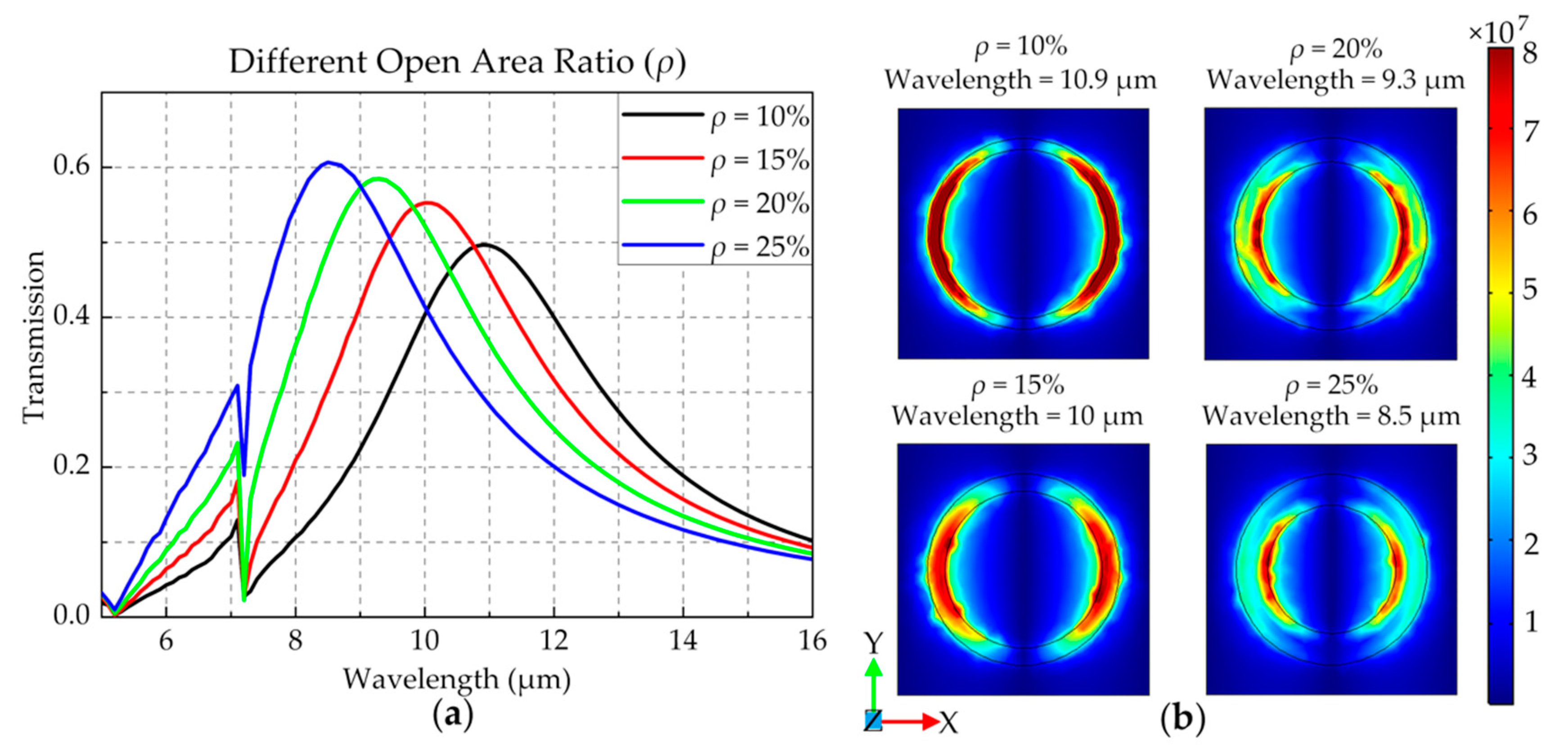
For Structure A, the effect of the geometric parameters on the optical transmission was systematically studied. Three transverse geometric parameters including r1, r2, and P were used to characterize the circular-coaxial apertures, as shown in Figure 1a. The open area ratio ρ is defined as ρ = π(r22- r12)/P2, which can affect the frequency and intensity of the LSPR. In order to verify the effect of changes of ρ, r2 and P were set as 0.75 μm and 2.0 μm, respectively. The transmission spectra of four different open area ratios from 10% to 25% were calculated, as shown in Figure 4a. As ρ increased, the transmission peak, dominated by the LSPR, was blueshifted from 10.9 μm to 8.5 μm, which was induced by the decrease of the diameter of the center circle. Figure 4b shows the electric-field distributions of four different ρ structures at their transmission peaks. It can be seen that the electric-field enhancement excited by the LSPR is located in the annular area without any gold. The strongest region of electric-field enhancement was near the center circle. In other words, the resonant frequency is mainly determined by the diameter of the center circle. Therefore, r1 decreases with the increase of ρ, which results in the blueshift of the transmission spectrum. As the four structures had the same P, their SPRs all occurred at about 7 μm, which conformed to the theory in Equation (4). The enhanced coupling between the LSPR and SPR resulted in a maximum transmission increase from 49.6% to 60.7%, as shown in Figure 4a. Considering the FWHM located at the LWIR region, it is appropriate to control ρ to be about 15%.
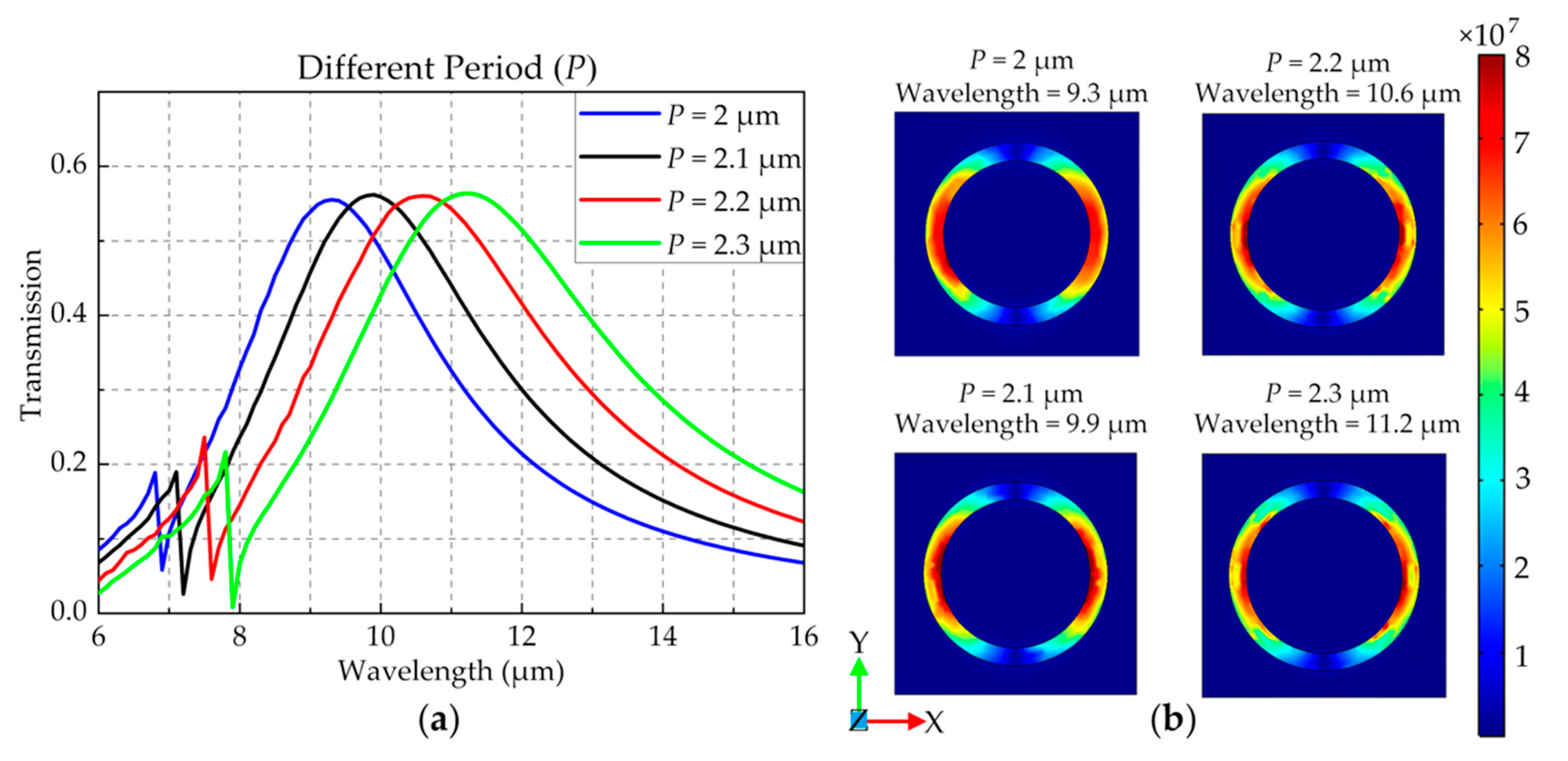
The influence of period P on the transmission spectra was also studied. Based on the above results, the open area ratio ρ was fixed at 16%. With the increase of P, r1 and r2 were simultaneously increased to ensure the same ρ. Figure 5a shows the transmission spectra of four different periods, and their maximum transmissions were almost 56%. This phenomenon resulted from a minor difference in the electric-field intensity for the four different periods, as shown in Figure 5b. Furthermore, the transmission peak redshifted with the increase of P, due to an increase of r1 resulting in the redshift of the LSPR resonant peak. As P increased from 2 μm to 2.3 μm, the FWHM increased from 3.6 μm to 4.7 μm. The observed Fano line shape at shorter wavelengths was due to the SPR by coupling between the incident light and Au–Si interface. It redshifted as P increased, which was dominated by period P. By considering the FWHM as well as its location, the period P was optimally designed as 2.1 μm, and the wavelength of its FWHM ranged from 8.2 μm to 12.1 μm, which covered almost the full LWIR region.
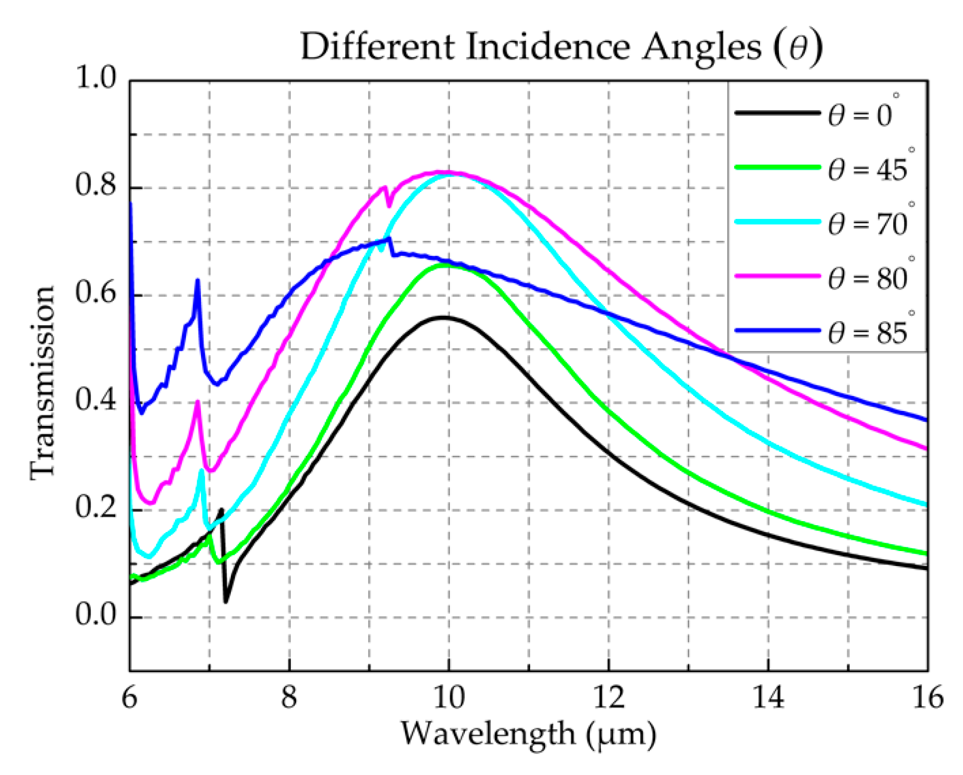
The effect of the incident angle θ on the transmission spectra was simulated, as shown in Figure 6. The maximum transmission increased from 55.5% to 83.0% as θ increased from 0° to 80°. It began to decrease with the further increase of θ. This phenomenon is contradictory to the widely held view that as the angle of incidence increases, transmission generally decreases and even total reflection occurs. The observed increase in the transmission is related to the Fabry–Perot resonance between the apertures. When light is incident at an angle, the gold on both sides of the aperture, together with the air in the middle, forms a Fabry–Perot resonance. Incidence light is bounced back multiple times in the Fabry–Perot cavity, which leads to the electric-field strength that is stronger than normal incidence. However, the illuminated depth of the gold aperture becomes smaller with the θ closer to 90°. As a result, the transmission enhanced by the Fabry–Perot resonance tends to disappear. The simulation results showed that the subwavelength structure has a large angle tolerance, which makes it suitable not only for vertical incident infrared, but also for infrared with incident angles ranging from 0° to 80°.

2.2. Electrical Transmission of the 3D Encapsulation Structure

In this work, the electrical transmission loss and feed-through characteristics of the proposed 3D encapsulation structure were optimally designed and calculated by the ANSYS HFSS 19.0 software (19.0, ANSYS Inc., Pittsburgh, PA, USA). A schematic view of the simulation structures of the feed-through and transmission loss is shown in Figure 7. Two channels mainly exist to cause the crosstalk between Port 1 and Port 2, which will result in significant attenuation for RF electrical signals. One channel is induced by the Pyrex-glass insulation and the silicon substrate, and the other channel is induced by the air dielectric between Port 1 and Port 2. A grounding substrate can make the coupling noise flow into the ground through the Pyrex-glass insulation, which is an effective method to suppress the coupling between the I/O ports. However, this also causes some energy leak for the RF signals.
In the ANSYS HFSS 19.0 software, four lumped ports were set as shown in Figure 7, which can be used to directly calculate the scattering parameters (S-parameters) at the ports. The silicon substrate was set as a reference plane to model the grounding. An air box, twice as large as the packaging cap, was designed to surround the packaging cap. The structural parameters are listed in Table 1. The sweep frequency was set from 0 GHz to 2 GHz with an interval of 0.01 GHz. The feed-through levels and transmission losses can be indicated by the transmission coefficients S21 between Port 1 and Port 2 and Port 1 and Port 1-1, respectively.
In Figure 8, the electrical performances of the proposed vertical silicon feedthrough were calculated and compared with two types of conventional TSVs. TSV A: The Cu feedthrough and SiO2 insulation layer were embedded in the low-resistance silicon substrate; TSV B: The same as TSV A, except that the substrate was intrinsic silicon. As shown in Figure 8a, the feed-through level of the silicon feedthrough was comparable with TSV B, and the feed-through level of TSV A was lower than the other structures due to the thin insulation layer as well as the grounded low-resistance silicon substrate inducing more energy loss. The feed-through levels were all far below the background-noise levels of the reported RF MEMS infrared detectors: −78 dB at 170 MHz, −62 dB at 833 MHz, and −60 dB at 1275 MHz [1,2]. Additionally, the transmission losses of the three structures are shown in Figure 8b. The transmission loss of the proposed silicon feedthrough was comparable with the TSV B within 1.7 GHz, and the transmission loss of the TSV A was much less than the other structures due to more energy loss. In order to further study the transmission loss of the silicon feedthrough, the impedance of about 1.9 Ω at 1 GHz was extracted using the ADS 2019 software (2019, Keysight Technologies Inc., Santa Rosa, CA, USA), which will have less effect on the signal transmission for RF MEMS infrared detectors. The results indicate that the silicon feedthrough has outstanding electrical performances that are comparable to conventional TSVs, which can provide low feed-through and low-loss electrical transmission for RF MEMS infrared detectors.
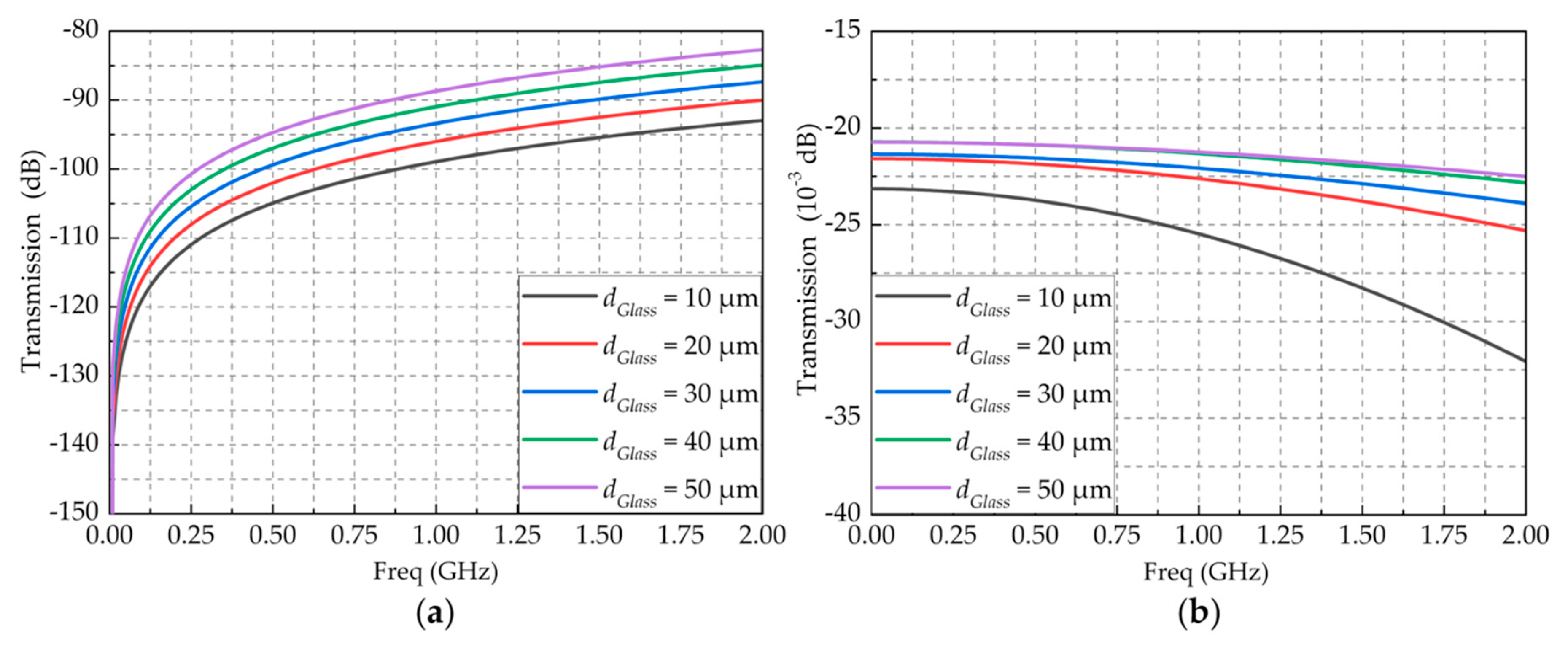
The insulation thickness dGlass of the proposed vertical silicon feedthrough is an important factor for the crosstalk as well as transmission loss. The radiating area of RF signals, from Port 1 to Port 2 through the air dielectric, increases with dGlass, which will induce an increase in the air dielectric capacitance. In this case, more energy will transfer from Port 1 to Port 2 through the air dielectric capacitance, which leads to an increase in the feed-through noise. As shown in Figure 9a, the maximum feed-through level increases from −93 dB to −82 dB with the increase of dGlass from 10 μm to 50 μm. And the impedance of air dielectric capacitance decreases with the signal frequency promoting, leading to an increase of the feed-through level. Besides, the grounded capacitance between the silicon feedthrough and silicon substrate reduces with the increase of dGlass, which can contribute to the improvement of S21 between Port 1 and Port 1-1. In Figure 9b, the minimum S21 promotes from −0.032 dB to −0.0225 dB within 2 GHz. This is due to a decrease in the grounded capacitance that contributes to a minor energy loss flowing into the ground. However, the reduced impedance of grounded capacitance, induced by the promotion of the signal frequency, caused a slight decrease of S21. The above results demonstrate that the proposed encapsulation structure has the ability to provide a high fidelity transmission of the RF signal for RF MEMS infrared detectors. It should be mentioned that the feed-through level, the transmission loss, the via size, and the micro-fabricated process should be considered in order to optimize the insulation thickness.

2.3. Thermal Stress of the 3D Encapsulation Structure

For the encapsulation of RF MEMS infrared detectors, thermal stress is an important issue that is critical to the reliability of the device, which can degrade the performance of the device. In this work, the maximum thermal stress curve of the proposed encapsulation structure was calculated by using the ANSYS Workbench 19.0 software (19.0, ANSYS Inc., Pittsburgh, PA, USA). A thermal condition was set at the whole simulation model of the packaging cap, which has a temperature rising from 0 to 200 °C within 200 seconds. The thermal condition generates a temperature zone and then forms a thermal diffusion throughout the model, which will result in the thermal stress induced by mismatched TECs. The material parameters in the thermal simulation are listed in Table 2.
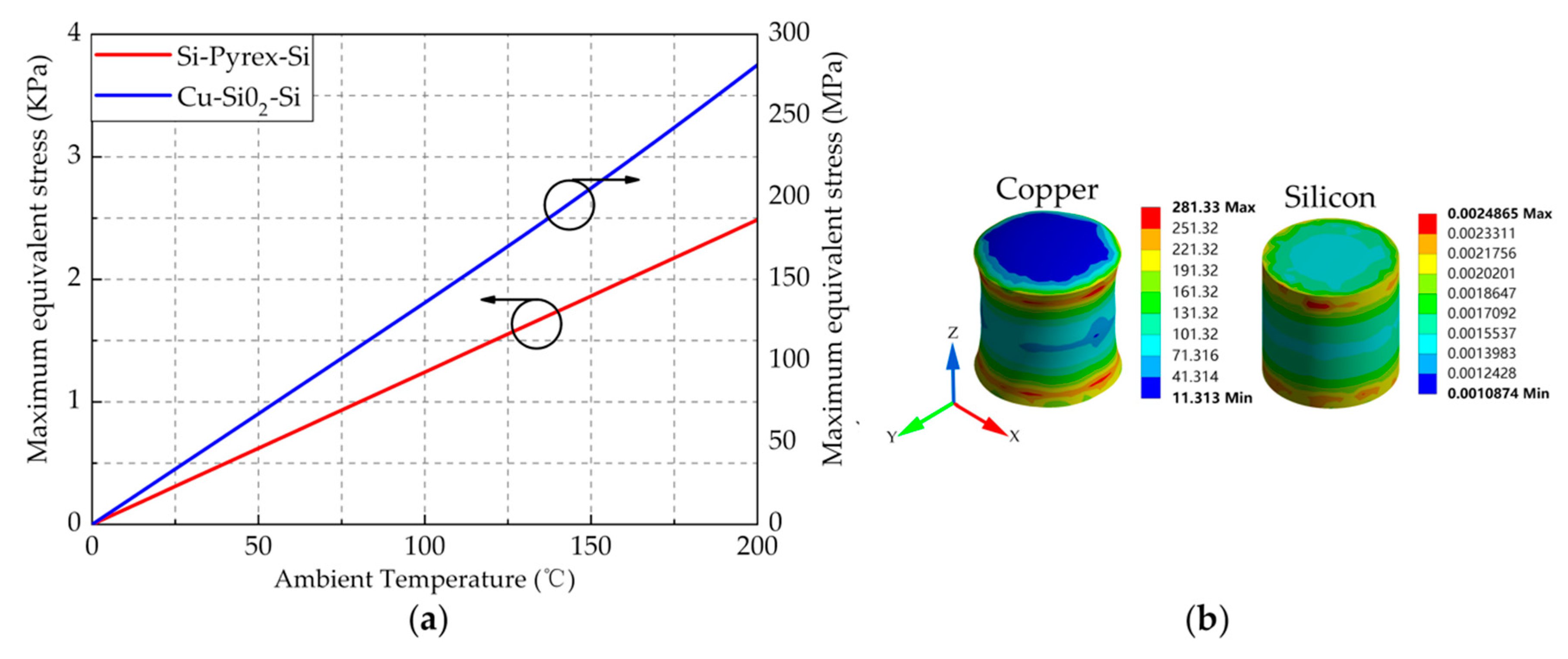
With the increase of ambient temperature from 0 to 200 °C, the maximum thermal stress of the proposed structure increased from 0 to 2.49 KPa, which is much less than that of a conventional TSV, as shown in Figure 10a. It can be seen from Table 2 that the TECs between the silicon and Pyrex glass are well matched, which contributes to the small thermal stress of the proposed structure. However, the TEC of Cu is about one order of magnitude higher than silicon or SiO2, which results in the conventional TSV having a maximum thermal stress of 281.33 MPa at a temperature of 200 °C. Figure 10b shows the strain distribution diagrams of the two structures at a temperature of 200 °C, which clearly shows that the thermal stress of the conventional TSV is much more than that of the proposed structure in this work. It was observed that the maximum strain positions occurred at the bottom and top interfaces of vias. This can result in a failure of soldered points, the insulation fracture, the performance degradation of devices, etc. Therefore, the above results confirm that the proposed 3D encapsulation structure has outstanding reliability to ensure the long-term operation of RF MEMS infrared detectors.

3. Conclusions

In this work, a novel wafer-level 3D encapsulation structure was designed for RF MEMS infrared detectors. The subwavelength structure with an array of circular-coaxial apertures was designed on the top of the packaging cap to achieve EOT and optical filtering capabilities at LWIR region. The vertical silicon feedthroughs, insulated by inserted Pyrex glass, were employed for the electrical interconnections.
The optical transmission properties of the proposed structure were systematically studied by COMSOL Multiphysics V4.3a software. The geometric parameters of circular-coaxial apertures with period and the open area rate were optimized to achieve a maximum transmission of up to 56% and the bandwidth of 3.9 μm, which have excellent optical filtering properties at the LWIR region. The maximum transmission can be further promoted with an increase of incident angle from 0° to 80°. The results also show that the subwavelength structure has a large incident angle tolerance.
In addition, the transmission loss and feed-through of the proposed structure was explored by using ANSYS HFSS 19.0 software. The simulated results showed that the feed-through level was lower than −82 dB, and the transmission coefficient S21 of one single via was more than −0.032 dB, which contributed to the low-loss electrical transmission for the RF MEMS infrared detectors. Furthermore, the thermal stress of the proposed structure was calculated by using the ANSYS Workbench 19.0 software. Compared with a conventional TSV structure, its thermal stress was much smaller at only 2.49 KPa at 200 °C, which demonstrates its outstanding reliability.
It can be concluded that the simulation results showed excellent performances of the proposed 3D encapsulation structure including high optical transmission, high optical filter, low-loss electrical transmission, and low thermal stress, which are desirable for RF MEMS infrared detector applications.

Author Contributions

J.Z. conceived the idea, designed the encapsulation structure, and wrote the manuscript. M.G. and C.S. performed the theoretical analysis, implemented the simulation, and contributed to the manuscript preparation. L.S. provided theoretical guidance. H.S. was responsible for formulating the research issues and revised the manuscript.

Funding

This research was funded by the National Natural Science Foundation of China, 61804084.

Acknowledgments

The authors would like to thank the editors and anonymous reviewers for their special efforts.

Conflicts of Interest

The authors declare no conflicts of interest.

References

  1. Hui, Y.; Gomez-Diaz, J.S.; Qian, Z.Y.; Alu, A.; Rinaldi, M. Plasmonic piezoelectric nanomechanical resonator for spectrally selective infrared sensing. Nat. Commun. 2016, 7, 11249. [Google Scholar] [CrossRef] [PubMed]
  2. Qian, Z.; Hui, Y.; Liu, F.; Kai, S.; Rinaldi, M. 1.27 GHz Graphene-Aluminum Nitride nano plate resonant infrared detector. In Proceedings of the 18th International Conference on Solid-State Sensors, Actuators and Microsystems, Anchorage, AK, USA, 21–25 June 2015; pp. 1429–1432. [Google Scholar]
  3. Kozlowski, L.J.; Arias, J.M.; Williams, G.M.; Vural, K.; Cooper, D.E.; Cabelli, S.A.; Bruce, C.F., Jr. Recent advances in staring hybrid focal plane arrays: Comparison of HgCdTe, InGaAs, and GaAs/AlGaAs detector technologies. Proc. SPIE 1994, 2274, 93–116. [Google Scholar]
  4. Rogalski, A. Infrared detectors: Status and trends. Prog. Quantum Electron. 2003, 27, 59–210. [Google Scholar] [CrossRef]
  5. Hotel, O.; Poli, J.P.; Mer-Calfati, C.; Scorsone, E.; Saada, S. A review of algorithms for SAW sensors e-nose based volatile compound identification. Sens. Actuat. B-Chem. 2018, 255, 2472–2482. [Google Scholar] [CrossRef]
  6. Candler, R.N.; Hopcroft, M.A.; Kim, B.; Park, W.-T.; Melamud, R.; Agarwal, M.; Yama, G.; Partridge, A.; Lutz, M.; Kenny, T.W. Long-Term and Accelerated Life Testing of a Novel Single-Wafer Vacuum Encapsulation for MEMS Resonators. J. Microelectromech. Syst. 2006, 15, 1446–1456. [Google Scholar] [CrossRef]
  7. Chen, K.-L.; Wang, S.S.; Salvia, J.C.; Melamud, R.; Howe, R.T.; Kenny, T.W. Wafer-Level Epitaxial Silicon Packaging for Out-of-Plane RF MEMS Resonators with Integrated Actuation Electrodes. IEEE Trans. Compon. Packag. Manuf. Technol. 2011, 1, 310–317. [Google Scholar] [CrossRef]
  8. Lim, Y.Y.; Chen, B.T.; Yu, A.B.; Shi, J.L. A broadband 3D package for RF MEMS devices utilizing through silicon vias (TSV). In Proceedings of the 16th International Conference on Solid-State Sensors, Actuators and Microsystems, Beijing, China, 5–9 June 2011; pp. 406–409. [Google Scholar]
  9. Wang, Z.Y. 3-D Integration and Through-Silicon Vias in MEMS and Microsensors. J. Microelectromech. Syst. 2015, 24, 1211–1244. [Google Scholar] [CrossRef]
  10. Arab, J.; Mishra, D.K.; Kannojia, H.K.; Adhale, P.; Dixit, P. Fabrication of multiple through-holes in non-conductive materials by Electrochemical Discharge Machining for RF MEMS Packaging. J. Mater. Process. Tech. 2019, 271, 542–553. [Google Scholar] [CrossRef]
  11. Zoschke, K.; Manier, C.-A.; Wilke, M.; Oppermann, H.; Ruffieux, D.; Dekker, J.; Jaakkola, A.; Pizza, S.D.; Allegato, G.; Lang, K.-D. Application of TSV integration and wafer bonding technologies for hermetic wafer level packaging of MEMS components for miniaturized timing devices. In Proceedings of the 65th International Conference on Electronic Components and Technology, San Diego, CA, USA, 26–29 May 2015; pp. 1343–1350. [Google Scholar]
  12. Marauska, S.; Claus, M.; Lisec, T.; Wagner, B. Low temperature transient liquid phase bonding of Au/Sn and Cu/Sn electroplated material systems for MEMS wafer-level packaging. Microsyst. Technol. 2013, 19, 1119–1130. [Google Scholar] [CrossRef]
  13. Jin, J.Y.; Yoo, S.; Yoo, B.W.; Kim, Y.K. Characterisation of silicon through-vias for wafer-level interconnection with glass reflows. Electron. Lett. 2012, 48, 1354–1355. [Google Scholar] [CrossRef]
  14. Zhang, M.; Yang, J.; He, Y.R.; Yang, F.; Yang, F.H.; Han, G.W.; Si, C.W.; Ning, J. Research on a 3D Encapsulation Technique for Capacitive MEMS Sensors Based on Through Silicon Via. Sensors 2019, 19, 93. [Google Scholar] [CrossRef] [PubMed]
  15. Haque, R.M.; Wise, K.D. A Glass-in-Silicon Reflow Process for Three-Dimensional Microsystems. J. Microelectromech. Syst. 2013, 22, 1470–1477. [Google Scholar] [CrossRef]
  16. Yu, H.; Rinaldi, M. Fast and high resolution thermal detector based on an aluminum nitride piezoelectric microelectromechanical resonator with an integrated suspended heat absorbing element. Appl. Phys. Lett. 2013, 102, 093501. [Google Scholar]
  17. Su, W.T.; Li, B.; Liu, D.Q.; Zhang, F.S. Characterization and application of cerium fluoride film in infrared antireflection coating. Infrared Phys. Technol. 2009, 52, 204–207. [Google Scholar] [CrossRef]
  18. Wu, H. Cost-effective double-layer antireflection coatings in mid-wavelength infrared band. Infrared Phys. Technol. 2014, 67, 473–476. [Google Scholar] [CrossRef]
  19. Wang, Y.K.; Hong, X.R.; Yang, G.F.; Sang, T. Filtering characteristics of a graphene ribbon with a rectangle ring in infrared region. AIP Adv. 2016, 6, 115311. [Google Scholar] [CrossRef] [Green Version]
  20. Kildishev, A.V.; Boltasseva, A.; Shalaev, V.M. Planar Photonics with Metasurfaces. Science 2013, 339, 1232009. [Google Scholar] [CrossRef] [Green Version]
  21. Jaksic, Z.; Smiljanic, M.M.; Vasiljevic-Radovic, D.; Obradov, M.; Radulovic, K.; Tanaskovic, D.; Krstajic, P.M. Field localization control in aperture-based plasmonics by Boolean superposition of primitive forms at deep subwavelength scale. Opt. Quant. Electron. 2016, 48, 225. [Google Scholar] [CrossRef]
  22. Niu, K.K.; Huang, Z.X.; Fang, M.; Li, M.Q.; Li, X.H.; Wu, X.L. Coupling of Gain Medium and Extraordinary Optical Transmission for Effective Loss Compensation. IEEE Access 2018, 6, 14820–14826. [Google Scholar] [CrossRef]
  23. Gao, H.; Zheng, Z.Y.; Chen, S.J.; Hao, H.Y. Achieving enhanced mid-infrared transmission through subwavelength periodic structures via redshift effect of the extraordinary optical transmission. J. Mod. Opt. 2014, 61, 766–772. [Google Scholar] [CrossRef]
  24. Ruan, H.X.; Shuang, Y.; Wang, L.G.; Li, L.L. Calculation of the Transmission Through a Rectangular Hole Filled with an Extreme Uniaxial Metamaterial. IEEE Trans. Antenn. Propag. 2018, 66, 6414–6419. [Google Scholar] [CrossRef]
  25. Tanaka, S.J. Wafer-level hermetic MEMS packaging by anodic bonding and its reliability issues. Microelectron. Reliab. 2014, 54, 875–881. [Google Scholar] [CrossRef]
  26. Lei, C.X.; Chen, L.Y.; Tang, Z.X.; Li, D.Y.; Cheng, Z.Z.; Tang, S.L.; Du, Y.W. Enhancement of magneto-optical Faraday effects and extraordinary optical transmission in a tri-layer structure with rectangular annular arrays. Opt. Lett. 2016, 41, 729–732. [Google Scholar] [CrossRef] [PubMed]
  27. Behera, G.; Ramakrishna, S.A. Enhanced broadband transmission through structured plasmonic thin films for transparent electrodes. J. Nanophotonics 2014, 8, 083889. [Google Scholar] [CrossRef]
  28. Ordal, M.A.; Bell, R.J.; Alexander, R.W.; Long, L.L.; Querry, M.R. Optical properties of Au, Ni, and Pb at submillimeter wavelengths. Appl. Opt. 1987, 26, 744–752. [Google Scholar] [CrossRef]
  29. Lynch, D.W.; Hunter, W.R. Handbook of Optical Constants of Solids, An Introduction to the Data for Several Metals; Academic Press: Salt Lake, UT, USA, 1997; Volume 2, pp. 341–419. [Google Scholar]
  30. Xiao, S.S.; Peng, L.; Mortensen, N.A. Enhanced transmission of transverse electric waves through periodic arrays of structured subwavelength apertures. Opt. Express 2010, 18, 6040–6047. [Google Scholar] [CrossRef] [PubMed] [Green Version]
  31. Zayats, A.V.; Smolyaninov, I.I.; Maradudin, A.A. Nano-optics of surface plasmon polaritons. Phys. Rep. 2005, 408, 131–314. [Google Scholar] [CrossRef]
  32. Zhang, M.; Huang, C.P.; Wang, G.D.; Zhu, Y.Y. Theory of extraordinary light transmission through sub-wavelength circular hole arrays. J. Opt. 2010, 12, 015004. [Google Scholar] [CrossRef]
  33. Krishnan, A.; Thio, T.; Kim, T.J.; Lezec, H.J.; Ebbesen, T.W.; Wolff, P.A.; Pendry, J.; Martin-Moreno, L.; Garcia-Vidal, F.J. Evanescently coupled resonance in surface plasmon enhanced transmission. Opt. Commun. 2001, 200, 1–7. [Google Scholar] [CrossRef]
  34. Degiron, A.; Ebbesen, T.W. The role of localized surface plasmon modes in the enhanced transmission of periodic subwavelength apertures. J. Opt. A Pure Appl. Opt. 2005, 7, S90–S96. [Google Scholar] [CrossRef]
Figure 1. (a) Schematic view and (b) sectional view of the structure of the proposed three-dimensional (3D) packaging cap. The period, inner radius, and external radius of the circular-coaxial apertures are labeled as P, r1, and r2, respectively.
Electronics 08 00974 g001
Figure 2. The model schematic of the subwavelength aperture structure for the optical simulations.
Electronics 08 00974 g002
Figure 3. (a) Transmission spectra and (b) electric-field distribution maps of Structure A and Structure B.
Electronics 08 00974 g003
Figure 4. (a) Transmission spectra of four different ρ structures; (b) The electric-field distribution maps of four different ρ structures at their transmission peaks.
Electronics 08 00974 g004
Figure 5. (a) Transmission spectra of four different periods with the fixed ρ of 16%; (b) The electric-field distribution maps of the four different periods at the maximum transmissions.
Electronics 08 00974 g005
Figure 6. Transmission spectra of five different incident angles. The parameters used for the calculation were P = 2.1 μm and ρ = 16%.
Electronics 08 00974 g006
Figure 7. Schematic view of the simulation structures.
Electronics 08 00974 g007
Figure 8. (a) Feed-through levels and (b) transmission losses of the proposed silicon feedthrough and two typical TSV structures.
Electronics 08 00974 g008
Figure 9. (a) Feed-through levels and (b) transmission losses of the proposed silicon feedthrough with different insulation thicknesses.
Electronics 08 00974 g009
Figure 10. (a) The calculated maximum thermal stress curves of the proposed encapsulation structure and the encapsulation structure with TSV; (b) the strain distribution diagrams of the two structures at a temperature of 200 °C.
Electronics 08 00974 g010
Table 1. Structural parameters in electrical simulations.
StructureFeedthrough ConductivityFeedthrough RadiusSubstrate ConductivityInsulation Thickness
This work1 × 105 S/m50 μm1 × 105 S/m50 μm
TSV A5.8 × 107 S/m50 μm1 × 105 S/m1 μm
TSV B5.8 × 107 S/m50 μm0 S/m1 μm
Table 2. Material parameters in thermal simulations.
MaterialSiCuPyrex GlassSiO2
Density (kg/m3)5050830022302220
TEC (1/°C)2.81 × 10−61.80 × 10−53.25 × 10−60.5 × 10−6
Young’s Modulus (Pa)1.30 × 10111.10 × 10119.10 × 1067.31 × 106
Poisson’s ratio0.280.340.20.17
Thermal Conductivity (W/(m∙°C))1254011.131.5