Abstract
A novel offset and finite-gain compensated differential switched-capacitor(SC) amplifier is presented. Incorporating the correlated double sampling (CDS) technique and input correlated level shifting (CLS) technique together, the DC offset and DC gain error of SC amplifier are further reduced by a factor of op-amp DC gain compared with the conventional offset and finite-gain compensated SC amplifier. The effectiveness of the new scheme has been analyzed and verified by extensive simulations. An SC amplifier with the proposed scheme is designed in 130 nm CMOS technology. Simulated results show that with an op-amp having a low DC gain of 30 dB and an input offset of 10 mV, the proposed SC amplifier achieves an output offset and DC-gain error of 154 µV and 0.05%, respectively, which are significantly improved compared with 1.155 mV and 0.42% achieved in the conventional SC amplifier.
1. Introduction
The switched-capacitor (SC) amplifier is widely used in various low-power, high-precision analog circuits, such as sample-and-hold circuits [1,2], instrumentation amplifiers for intelligent sensors in strain, pressure and temperature measurement [3], micro-electromechanical systems (MEMS) capacitive accelerometers [4], multi-parameter sensing micro-systems [5], and readout amplifiers for biomedical signal acquisition systems [6,7,8]. Those amplifiers should have a very low DC offset and DC gain error as the output signals detected by the sensors are low-frequency and low-level. Nevertheless, the performance of an SC amplifier is limited by several non-ideal effects, among which the finite DC gain of the op-amp is the most important one, which affects the amplifier’s output DC offset and gain error more seriously than other factors.
Temes, Martin, and Haug [9,10] proposed offset and finite-gain compensated SC amplifiers for low-frequency inputs in both single-ended and differential architectures. With the correlated double sampling (CDS) switching of the input capacitor and an output capacitor, the DC gain error is reduced and proportional to A−2, and the output DC offset is reduced by a factor of A, where A is the DC gain of the op-amp. Therefore, the DC offset and DC gain error can only be further reduced by increasing the DC gain of the op-amp, which presents a difficulty for designing low-power, highly accurate analog circuits, especially at a low supply voltage for IoT and portable applications.
Recently, several techniques have been developed to alleviate the finite gain error of op-amps in SC circuits, such as comparator-based SC (CBSC) circuits [11,12], digital circuits-based SC circuits, which are also called zero-crossing-detectors-based (ZCD) SC circuits [13,14,15] and digital calibration algorithms [16,17,18]. However, CBSC circuits introduce large offset errors and linearity problems due to the output overshoots and voltage drop on switches [19]. Furthermore, these digital techniques are more complicated than switched-capacitor techniques, which have been proposed to increase the effective gain of op-amps, such as correlated level shifting (CLS) [20], cross-coupling CLS [21], sequential-CLS [22], charge-compensated CLS [23], and averaging-CLS [24]. The CLS technique has gained popularity in pipelined ADCs to reduce the gain error of residue amplifiers [20,21,24,25,26] and in inverter-based delta-sigma modulator to enhance the DC gain of the first stage integrator [27]. However, those CLS techniques are applied to the output of the op-amps, one CLS operation only makes the DC gain error proportional to A−2 [20,27], while two CLS operations make the DC gain error proportional to A−3 [25] at the expense of increased current consumption for accurate settling within a reduced settling time. Moreover, the CLS technique does not remove offset when applied to the output of op-amp [20,21], unlike the CDS technique does [10,28,29].
Therefore, we propose a novel scheme combing the CDS technique and input CLS technique for SC amplifier to enhance the accuracy as well as to further reduce the offset even with low op-amp gain. Note that the concept of using CDS in combination with input CLS is first introduced in this paper. Unlike the concept of combining the chopper stabilization (CS) and output CLS techniques proposed in [30], the input CLS technique helps to reduce the DC offset as well as the DC gain error. It is based on the fact that reducing the amount of residue charge on the input capacitor helps the SC amplifier make a complete charge transfer from the input capacitor to the output capacitor. The rest of the paper is organized as follows. In Section 2, the conventional SC amplifier with CDS method is reviewed and the proposed input CLS-based SC amplifier structure is detailed and analyzed. The effectiveness of the new scheme has been analyzed and verified by extensive behavioral simulations compared with the conventional design of [10]. In Section 3, implementation details of the building block circuits are presented and simulation results are discussed as well. Section 4 draws the conclusions.
2. Input CLS-Based Switched-Capacitor Amplifier
2.1. Conventional CDS-Based SCAmplifier
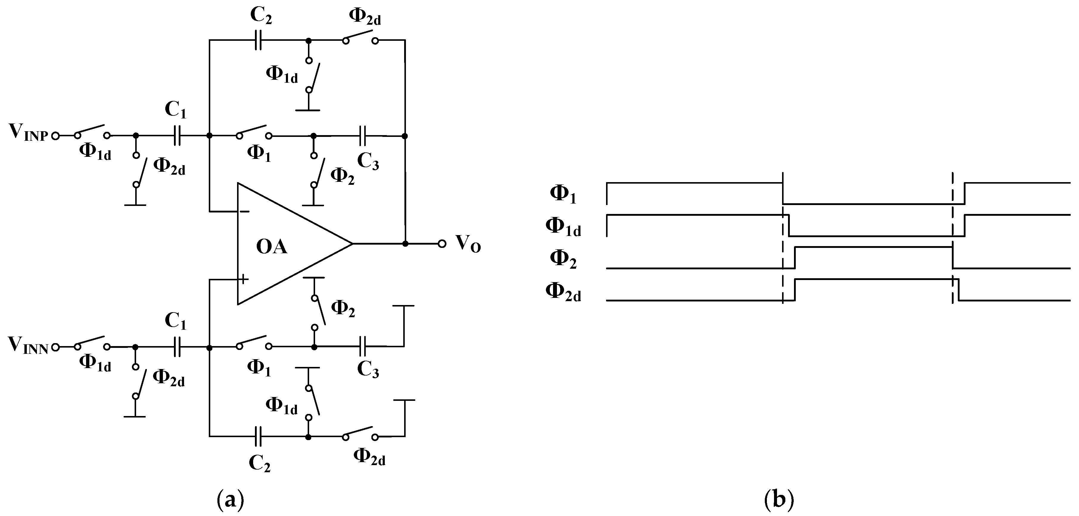
Figure 1 shows the operation of the well-known differential SC amplifier [10]. Φ1 and Φ2 are two non-overlapping clock phases, while Φ1 and Φ2 cut off earlier than Φ1d and Φ2d respectively. During Φ1, the differential input signals, as well as the offset and flicker noise, are sampled onto C1, while the output voltage only changes by the op-amp input offset. During Φ2, the charge is transferred from C1 to C2 through the feedback loop formed by C2 and the op-amp.
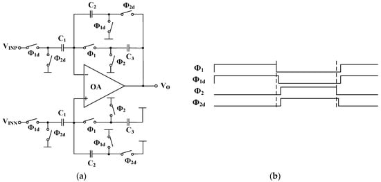
Figure 1.
Conventional offset and finite-gain compensated switched-capacitor (SC) amplifier (a) switching scheme; (b) Φ1 and Φ2 are non-overlapping clocks, and Φ1d and Φ2d cut off later than Φ1 and Φ2, respectively, for bottom-plate sampling.
According to [31], the transfer function of this amplifier at low frequency and DC output offset are given by the following Equations (1) and (2):
where , is input referred offset of op-amp, A is the DC gain of op-amp. However, due to its finite DC gain, the op-amp sees a difference of between its input terminals, which results in a DC gain error and a DC offset of the SC amplifier to be proportional to A−2 and A−1, respectively.
2.2. Input CLS-Based Offset and Finite-Gain Compensated SC Amplifier
Figure 2a shows the schematic of the proposed SC amplifier. There are two main non-overlapping phases Φ1 (sample) and Φ2 (amplification). The phase Φ2 is divided into two sub-phases: Φ21 and Φ22, during which the CDS operation and CLS operation occur, respectively, as shown in Figure 2b. During Φ1, the input signal is sampled by C1, while the offset is stored on COS. During Φ21, the amplifier enters the CDS amplification phase. The charge is transferred from C1 to C2 with offset and DC gain error nearly the same as the conventional design, while the offset and the finite-gain induced error at the op-amp’s input are stored on CCLS, whose bottom plate is connected to VCM. During Φ22, the bottom plate of CCLS that is connected to the node X is shifting towards VCM (virtual ground) by charge conservation of CCLS. Therefore, the residue charge stored on C1 is reduced from to , where and are the output voltage in phase Φ21 and Φ22, respectively, and n is the discrete time index. Consequently, the charge transfer from C1 to C2 is more complete than the conventional technique in [10].
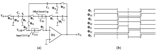
Figure 2.
Input correlated level shifting (CLS)-based SC amplifier in single-ended architecture: (a) schematic diagram; (b) timing scheme.
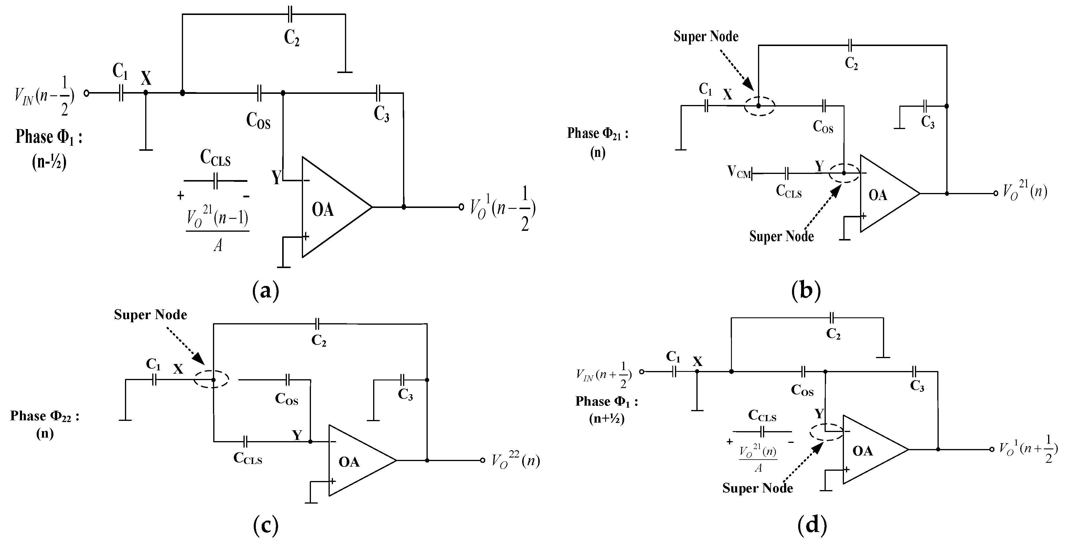
Figure 3 shows the detailed sample, CDS operation and CLS operation steps during phase Φ1, Φ21 and Φ22, respectively. Here the even clock period n − i (i = 0, 1, 2, ...) corresponds to the Φ2 phase and the odd clock period n – i/2 (i = 1, 3, 5, ...) corresponds to the Φ1 phase. Figure 3a shows the sample step during Φ1 at clock period n − 1/2, input signal is sampled by C1 and C2 is discharged, the charge stored at CCLS is . Considering the finite DC gain of op-amp, and node X and Y are treated as super nodes, as shown in Figure 3b, the following Equations (3) and (4) can be derived according to nodal charge analysis to show the voltage relations of the circuit at the end of Φ21 within clock period n.
where represents the voltage of node X in phase Φ21, and represents the output voltage in phase Φ1.
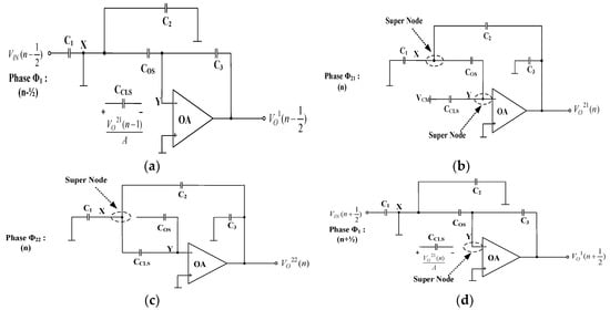
Figure 3.
Detailed operation scheme of the proposed SC amplifier: (a) sample step during Φ1 at clock period n – ½; (b) Correlated double sampling (CDS) operation step during Φ21 at clock period n; (c) CLS operation step during Φ22 at clock period n; (d) sample step during Φ1 at clock period n+1/2.
At the beginning of phase Φ22, the bottom plate of CCLS is connected to node X as shown in Figure 3c, the correlated level shifting operation occurs, and the voltage relations of the circuit at the end of Φ22 can be obtained by charge conservation of CCLS and nodal charge analysis as Equations (5) and (6) shown below:
where and represent the voltage of node X and the output voltage in phase Φ22 respectively.
According to Equations (3)–(6), we can derive the following Equation (7):
For low frequency especially DC input, when output voltage arrives its final value, then Equation (4) and Equation (7) can be simplified to the following Equations (8) and (9):
Obviously seen from Equation (9), the gain error is proportional to the correlated output voltage differences at the end of phase Φ22 and Φ21.
As shown in Figure 3d, node Y is treated as super node, then charge conservation in this super node implies the following Equation (10) during Φ1 at clock period n + 1/2.
Choosing , Equation (10) can be simplified as Equation (11):
For DC input, when the output voltage reaches the final value. Therefore by substituting Equation (8) into Equation (11), and Equation (4) into Equation (3), the following Equations (12) and (13) are obtained:
Finally, the transfer function of this amplifier at low frequency can be given by the following Equation (14), according to Equation (9), Equation (12) and Equation (13).
Seen from the denominator of Equation (14), the DC gain error becomes proportional to A−3 rather than A−2.
Besides reducing the DC gain error caused by the finite DC gain of the op-amp, the proposed scheme can also reduce the DC offset significantly. Similar to the above DC gain error analysis, the output DC offset can also be determined by the same method. Considering the input referred offset of the op-amp VOS as shown in Figure 4, the following Equations (15)–(18) can be derived according to nodal charge analysis and charge conservation of CCLS to show the voltage relations of the circuit at the end of phase Φ21, Φ22 and Φ1.
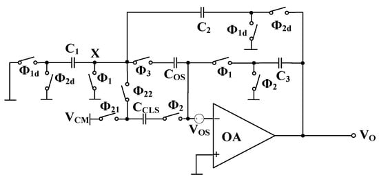
Figure 4.
Schematic of the proposed SC amplifier with input referred offset.
Note that Equation (5) is still effective at the end of phase Φ22 for DC offset analysis. Choosing , Equation (18) can be simplified as Equation (19):
For DC offset analysis, , when the output voltage reaches its final value. Therefore according to Equation (5), Equations (15)–(17), and Equation (19), we can obtain the following simplified Equations (20)–(22):
Thus the output DC offset can be deduced from Equations (20)–(22) and is given by Equation (23):
According to Equation (23), the output DC offset of SC amplifier is approximately , which is proportional to A−2 but not A−1.
From the above analysis, the proposed scheme for SC amplifier reduces the output DC offset and DC gain error each to times of those in the conventional design in [10].
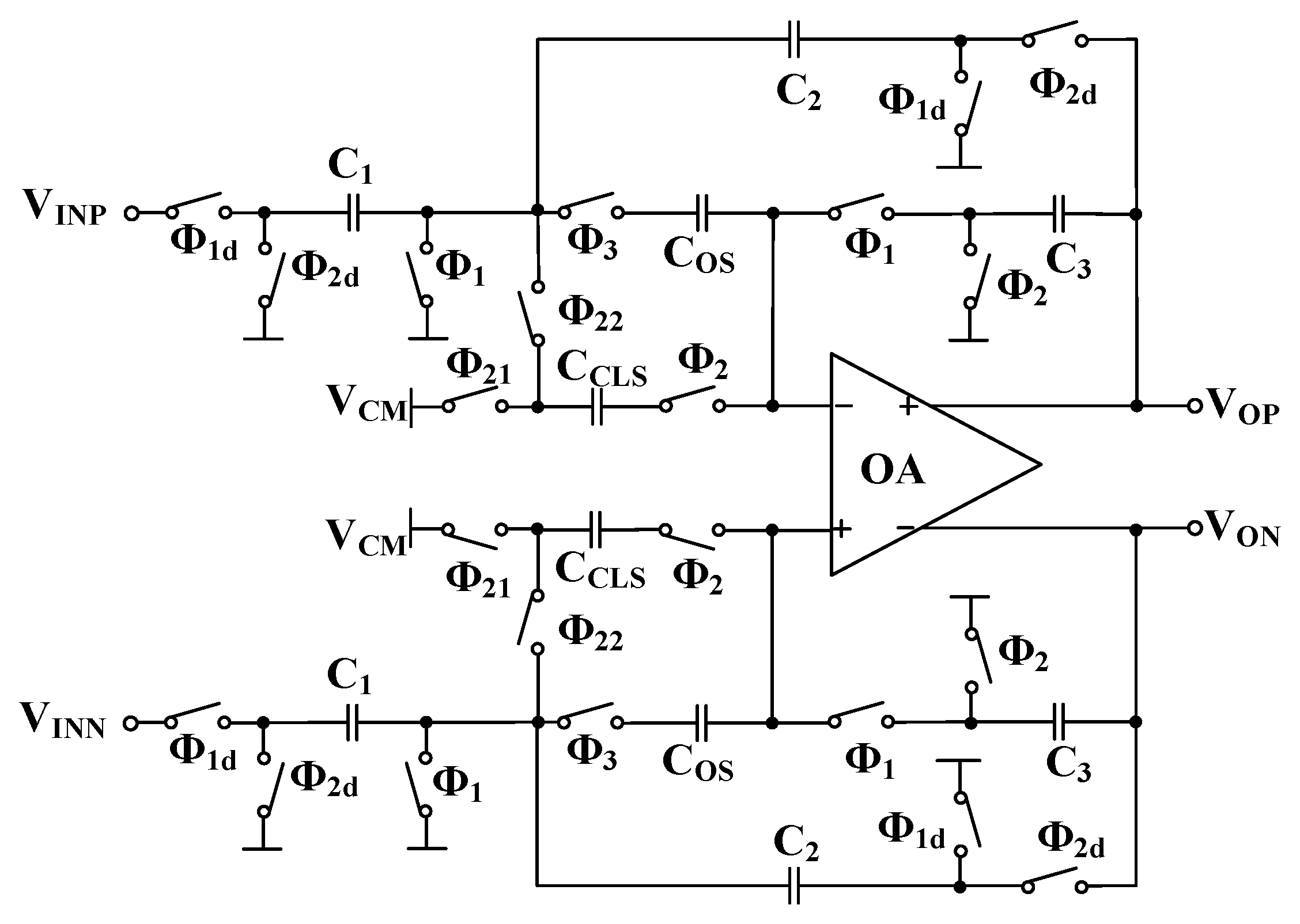
The proposed SC amplifier can also be implemented in differential architecture as shown in Figure 5. The transfer function of this amplifier at low frequency and output DC offset are the same as Equation (14) and Equation (23), respectively, where , , and are the output differential signals in phase Φ22.

Figure 5.
Differential architecture of the proposed SC amplifier.
2.3. Simulation Results
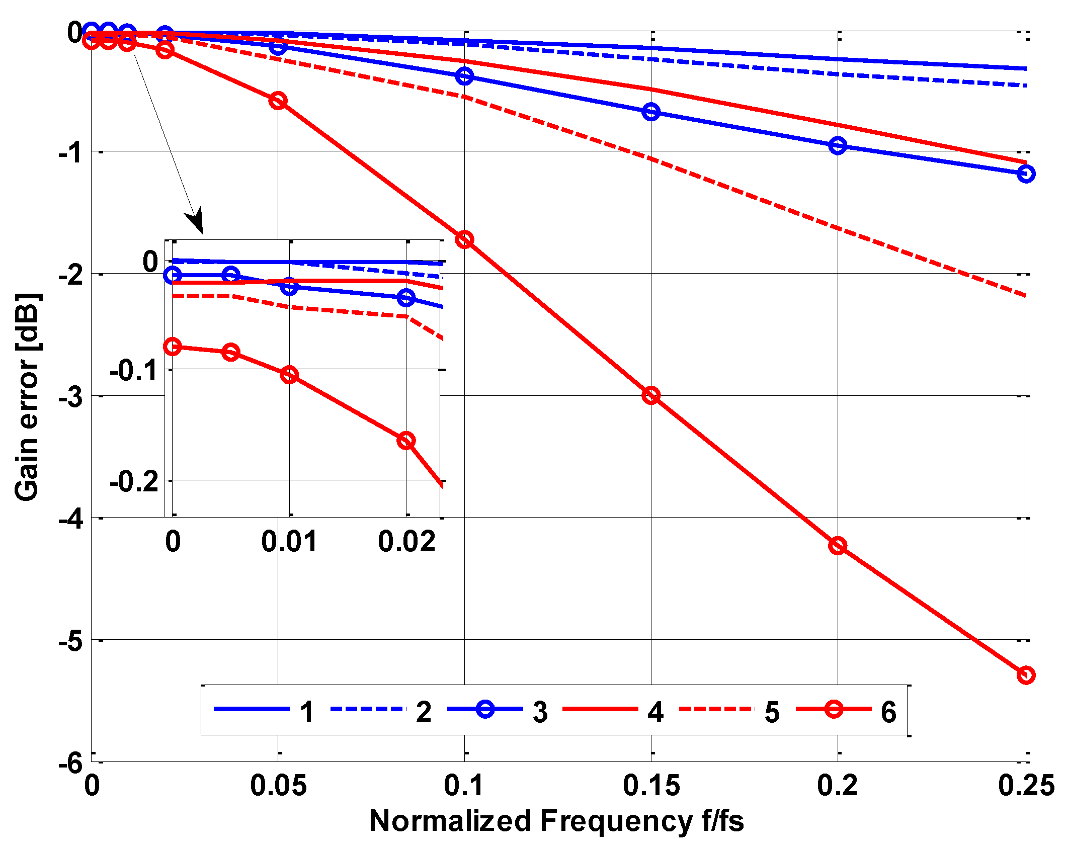
The normalized gain error as a function of frequency is plotted in Figure 6, which compares with the gain error of the conventional SC amplifier for nominal gains of unity, three and nine respectively in behavioral simulation by using block-level models in Cadence Spectre. Both of the two SC amplifiers are in differential architecture. The switches and op-amp are both using behavioral models. The op-amp is assumed to have 30 dB DC gain. As the curves illustrate, the DC gain error of the proposed design is smaller than the conventional one and the improvement is substantial for higher nominal gain cases. It can also be seen that the frequency responses of the proposed design are superior to the conventional one, e.g., the gain error of the new design is smaller than 1.2 dB for frequency up to fs/4, where fs is sampling frequency, while that of the conventional design is 5.3 dB, for a nominal gain of nine.
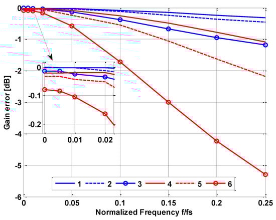
Figure 6.
The normalized gain error versus frequency curves of the proposed and conventional SC amplifier in [10] for nominal gains of (1) and (4) unity, (2) and (5) three, (3) and (6) nine, respectively, in behavioral simulation.
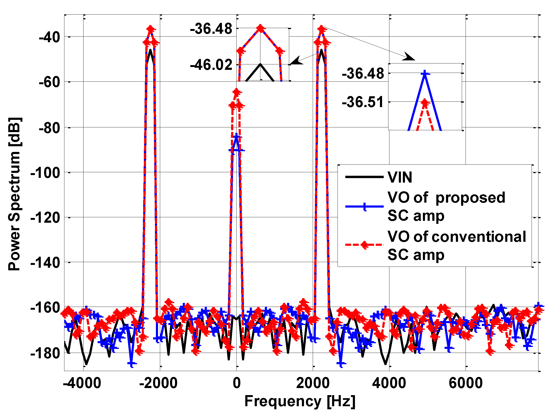
To verify the above analysis, circuit-level behavioral simulations were conducted on the conventional and proposed SC amplifier respectively. Both of the them are in differential architecture. Figure 7 shows the power spectrums of the proposed and conventional designs for a 2.246 kHz sinusoidal input signal (VIN = 20 mVpp,diff) with a nominal gain of three (, where the op-amp gain and input referred offset are assumed to be 30 dB and 10 mV, respectively. The theoretical output DC offset of the conventional and proposed designs are 1.2599 mV and 0.1237 mV, respectively, according to Equation (2) and Equation (23). The theoretical DC gain of conventional and proposed designs are 2.9880 (9.508 dB) and 2.9988 (9.538 dB), respectively, according to Equation (1) and Equation (14), which indicates the DC gain error is improved from 0.4% to 0.04%. It can be seen from the power spectrum curves that the output DC offset of the proposed design is around 20 dB lower than the conventional design, and the DC gain is improved from 9.51 dB to 9.54 dB for nominal gain of 3 (9.542 dB), which are in accordance with the theoretical analysis.
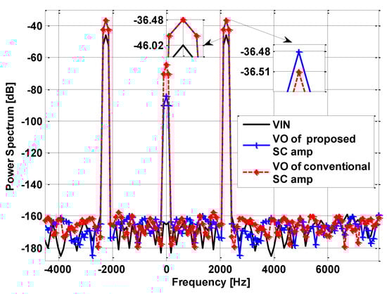
Figure 7.
Output power spectrums of the proposed and conventional SC amplifier with 10 mV op-amp input referred offset and 2.246 kHz, 20 mVpp,diff, sinusoidal input signal for a nominal gain of 3.
3. Circuit Implementation
To verify the effectiveness of the proposed scheme, the SC amplifier of Figure 5 is implemented in 130 nm CMOS triple-well process with metal-insulator-metal (MIM) capacitors and high-resistivity poly resistors. The conventional SC amplifier of Figure 1 is also realized for comparison. The switches are realized by NMOS transistors (W/L = 10 µm/0.12 µm). The capacitor sizes used in Figure 1 are , , while the capacitor sizes used in Figure 5 are , , , for a nominal gain of 3.
Figure 8 shows the schematic of the op-amp used in both SC amplifiers. It is a standard fully differential single-stage op-amp. The simulation results show that the amplifier achieves a 30.3 dB open-loop DC gain, 33 MHz UGF, and phase margin of 90° with 1.6 Pf load capacitor.
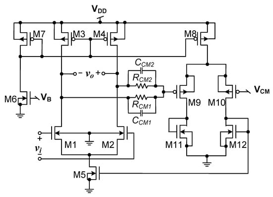
Figure 8.
Differential single-stage op-amp.
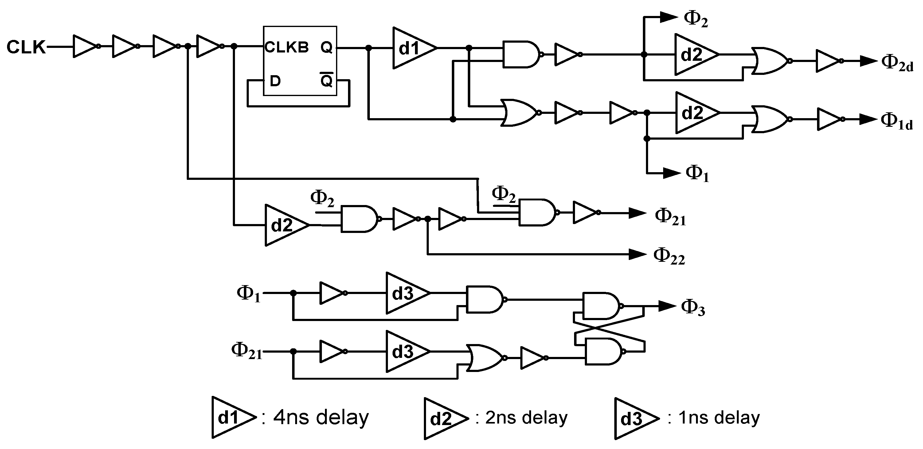
Figure 9 shows the clock generation circuit for generating the seven clock phases: two non-overlapping clock phases Φ1 and Φ2, two delayed clock phases Φ1d and Φ2d for charge injection elimination, Φ3 and sub-phase Φ21 for CDS amplification, sub-phase Φ22 for input correlated level shifting. The simulated non-overlapping time of Φ1 and Φ2 is 4 ns, and the non-overlapping time of Φ21 and Φ22 is 2 ns. Although the op-amp in Figure 5 is left open-loop during those non-overlapping intervals, the glitches appear at the output of op-amp at the clock transitions are eliminated due to the fully differential amplifier architecture. Note that the proposed SC amplifier requires more complicated timing schemes compared with the conventional one, which may lead to an increase of power consumption. However, the power consumption of the clock generator is around 1.67 µA for input CLK frequency of 800 kHz by transistor-level simulation. Hence, a further reduction of the power consumption of the clock generator can be achieved by optimizing the size of the logic cell. Furthermore, the maximum clock frequency is reduced compared with the conventional one. However, the proposed SC amplifier is aimed for low-frequency and low-level signal detection. Therefore, the effect of the reduced maximum sampling frequency is small.

Figure 9.
Clock generator circuit.
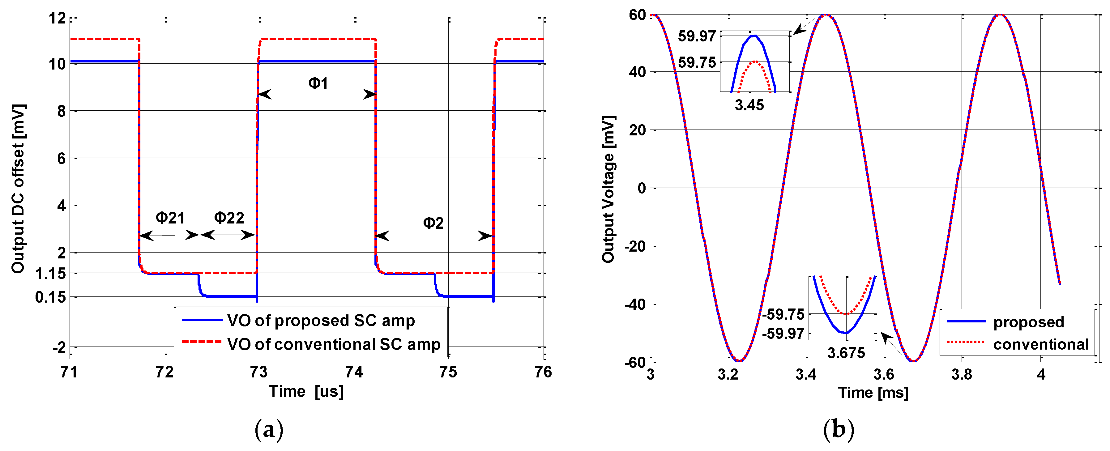
Figure 10 shows the simulated output waveforms of the proposed and conventional designs with a nominal gain of 3. The supply voltage VDD is 1.2 V and the VCM is 0.6 V. The clock signal CLK is at 800 kHz for generating 400 kHz clock signals of Φ1, Φ2, Φ3, Φ1d, and Φ2d, 800 kHz clock signals of Φ21 and Φ22. For output DC offset simulation, a voltage source of 10 mV is inserted at the inverting input terminal of the op-amp. It can be seen from Figure 10a that the output DC offset of the proposed design is 154 µV during Φ22, which is further reduced by a factor of 7.5 compared with the conventional design of 1.155 mV during Φ2. The Figure 10b shows the output waveforms for 2.246 kHz, 20 mVpp,diff sinusoidal input signal. The conventional SC amplifier output is 59.75 mV, while that of the proposed SC amplifier is 59.97 mV, much closer to the ideal output of 60 mV. Hence, the simulated DC gain error of the proposed design is 0.05%, which is significantly improved by a factor of 8.4 compared with the conventional design of 0.42%. Seen from the above simulation results, the output DC offset and DC gain error improvements of the proposed design are close to the theoretical value of compared with the conventional design.
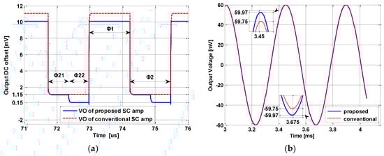
Figure 10.
Output waveforms of the proposed and conventional SC amplifier with 30 dB DC gain at a nominal gain of 3: (a) for 10 mV input referred offset of op-amp; (b) for 2.246 kHz, 20 mVpp,diff sinusoidal input signal.
A specification summary of simulation results are given in Table 1. The results show that the proposed SC amplifier achieves an output offset and DC-gain error of 154 µV and 0.05%, respectively with an op-amp of 30 dB DC gain and 10 mV input offset, which are significantly improved compared with the 1.155 mV and 0.42% achieved in the conventional SC amplifier. It can be also seen from Table 1 that the number of switches of the proposed SC amplifier is more than the conventional one, which may increase the layout area. However, this can be alleviated by optimizing the switches size.

Table 1.
Simulation results and comparison of SC amplifier.
Table 2 shows the comparison results with other reported SC amplifiers based on theoretical analysis. It can be easily found that the proposed SC amplifier achieves excellent performance in both output the DC offset and DC gain error.
Table 2.
With other reported SC amplifiers.
4. Conclusions
A novel offset and finite-gain compensation scheme that combines the CDS technique and the input CLS technique for SC amplifiers has been presented. The DC offset and DC gain error of the proposed design are proportional to A−2 and A−3, respectively, which are 1/A of those in the conventional SC amplifier of [10]. Compared with the CLS technique applied to the output of the op-amp, the proposed compensation scheme achieves a better performance in the output DC offset cancellation.
The effectiveness of the proposed design has been verified through the circuit level simulations by using a 130 nm CMOS process. The simulation results are in good agreement with the transfer function-based analysis.
Author Contributions
Conceptualization, Y.C. (Yan Chen) and Y.G.; methodology, Y.C. (Yan Chen) and Y.G.; validation, Y.C. (Yan Chen) and C.L.; formal analysis, Y.C. (Yan Chen) and Y.G.; investigation, Y.C. (Yan Chen), Y.C. (Yousheng Chen), and C.L.; resources, Y.C. (Yan Chen), Y.C. (Yousheng Chen), and Y.G.; writing—original draft preparation, Y.C. (Yan Chen); writing—review and editing, Y.C. (Yousheng Chen), C.L., and Y.G.; supervision, Y.C. (Yan Chen) and Y.C. (Yousheng Chen); project administration, Y.C. (Yan Chen); funding acquisition, Y.C. (Yan Chen) and Y.C. (Yousheng Chen).
Funding
This research was funded by National Natural Science Foundation of China, grant number61704113, the Science and Technology Basic Research Foundation of Shenzhen, grant number JCYJ20160527101842119, and Natural Science Foundation of Guangdong Province, grant number 2018A030313146.
Acknowledgments
The authors would like to thank K.-P.Pun from Department of Electronic Engineering, The Chinese University of Hong Kong, for his technical support. The authors thank the anonymous reviewers for their constructive comments.
Conflicts of Interest
The authors declare no conflict of interest.
References
- Shirin, P.; Jaime, R.A.; Alfonso, R.C.G.; Antonio, J.L.M.; Ramon, G.C. An amplified offset compensation scheme and its application in a track and hold circuit. IEEE Trans.Circuits Syst. II Exp. Briefs 2018, 65, 416–420. [Google Scholar]
- Yoshizawa, H.; Temes, G.C. Switched-Capacitor Track-and-Hold Amplifiers With Low Sensitivity to Op-Amp Imperfections. IEEE Trans. Circuits Syst. I Regul. Pap. 2007, 54, 193–199. [Google Scholar] [CrossRef]
- Koay, K.C.; Chan, P.K. A Low Energy-Noise 65nm CMOS Switched-Capacitor Resistive-Bridge Sensor Interface. IEEE Trans. Circuits Syst. I Regul. Pap. 2017, 64, 799–810. [Google Scholar] [CrossRef]
- Liu, Y.; Xiao, Y.; Fu, Q. A low power consumption inverter-based ΣΔ interface for capacitive accelerometer. IEICE Electron. Express 2018, 15, 1–16. [Google Scholar] [CrossRef]
- Suh, J.-H.; Park, J.-H.; Kweon, S.-J.; Yoo, H.-J. Multiparameter Sensor Interface Circuit With Integrative Baseline/Offset Compensation by Switched-Capacitor Level Shifting/Balancing. IEEE Trans. Circuits Syst. II Express Briefs 2018, 65, 316–320. [Google Scholar] [CrossRef]
- Trung, N.T.; Häfliger, P.; Nguyen, T.T. A Submicrowatt Implantable Capacitive Sensor System for Biomedical Applications. IEEE Trans. Circuits Syst. II Express Briefs 2015, 62, 209–213. [Google Scholar] [CrossRef]
- Nguyen, T.T.; Hafliger, P. An energy efficient inverter based readout circuit for capacitive sensor. In Proceedings of the IEEE Biomedical circuits and Systems Conference (BioCAS), Rotterdam, The Netherlands, 31 October–2 November 2013; pp. 326–329. [Google Scholar]
- Lee, J.; Johnson, M.D.; Kipke, D.R. A Tunable Biquad Switched-Capacitor Amplifier-Filter for Neural Recording. IEEE Trans. Biomed. Circuits Syst. 2010, 4, 295–300. [Google Scholar] [CrossRef] [PubMed]
- Temes, G.; Haug, K. Improved offset-compensation schemes for switched-capacitor circuits. Electron. Lett. 1984, 20, 508–509. [Google Scholar] [CrossRef]
- Martin, K.; Ozcolak, L.; Lee, Y.; Temes, G. A differential switched-capacitor amplifier. IEEE J. Solid-State Circuits 1987, 22, 104–106. [Google Scholar] [CrossRef]
- Fiorenza, J.K.; Sepke, T.; Holloway, P.; Sodini, C.G.; Lee, H.-S. Comparator-Based Switched-Capacitor Circuits for Scaled CMOS Technologies. IEEE J. Solid-State Circuits 2006, 41, 2658–2668. [Google Scholar] [CrossRef]
- Zamani, M.; Shahin, J.A.; Dousti, M.; Mohammad, N.M. A 12b, 40-MS/s, 4.1mW fully differential CBSC pipelined ADC in 0.18 µm CMOS. IEICE Electron. Express 2010, 7, 1714–1720. [Google Scholar] [CrossRef]
- Shin, S.K.; Rudell, J.C.; Daly, D.C.; Munoz, C.E.; Chang, D.Y.; Gulati, K.; Lee, H.S.; Straayer, M.Z. A 12 bit 200 MS/s Zero-Crossing-Based Pipelined ADC With Early Sub-ADC Decision and Output Residue Background Calibration. IEEE J. Solid-State Circuits 2014, 49, 1366–1382. [Google Scholar] [CrossRef]
- Brooks, L.; Lee, H.S. A 12b, 50 MS/s, Fully Differential Zero-Crossing Based Pipelined ADC. IEEE J. Solid-State Circuits 2009, 44, 3329–3343. [Google Scholar] [CrossRef]
- Min, D.J.; Shim, J.H. A Charge-Sharing-Based Two-Phase Charging Scheme for Zero-Crossing-Based Integrator Circuits. Electronics 2019, 8, 821. [Google Scholar] [CrossRef]
- Mafi, H.; Yargholi, M.; Yavari, M. Statistics-Based Digital Background Calibration of Residue Amplifier Nonlinearity in Pipelined ADCs. IEEE Trans. Circuits Syst. I Regul. Pap. 2018, 65, 4097–4109. [Google Scholar] [CrossRef]
- Montazerolghaem, M.A.; Moosazadeh, T.; Yavari, M. A Pre-Determined LMS Digital Background Calibration Technique for Pipelined ADCs. IEEE Trans. Circuits Syst. II Express Briefs 2015, 62, 841–845. [Google Scholar] [CrossRef]
- Fang, B.N.; Wu, J.T. A 10-Bit 300-MS/s Pipelined ADC With Digital Calibration and Digital Bias Generation. IEEE J. Solid-State Circuits 2013, 48, 670–683. [Google Scholar] [CrossRef]
- Jang, J.E. Comparator-based switched-capacitor pipelined ADC with background offset calibration. In Proceedings of the IEEE International Symposium of Circuits and Systems (ISCAS), Rio de Janeiro, Brazil, 15–18 May 2011; pp. 253–256. [Google Scholar]
- Gregoire, B.R.; Moon, U.-K. An Over-60dB True Rail-to-Rail Performance Using Correlated Level Shifting and an Opamp with 30dB Loop Gain. Dig. Tech. Pap. 2008, 43, 540–634. [Google Scholar]
- Musah, T.; Moon, U.K. Correlated level shifting technique with cross-coupled gain-enhancement capacitors. Electron. Letter 2009, 45, 672–674. [Google Scholar] [CrossRef]
- Tabasy, E.Z.; Kamarei, M.; Ashtiani, S.J.; Palermo, S. Sequential Correlated Level Shifting: A Switched-Capacitor Approach for High-Accuracy Systems. IEEE Trans. Circuits Syst. II Express Briefs 2013, 60, 857–861. [Google Scholar] [CrossRef]
- Abdelhamid, M.; Hussien, F.; Aboudina, M. Charge-compensated correlated level shifting for single-stage opamps. Electron. Lett. 2015, 51, 817–818. [Google Scholar] [CrossRef]
- Hung, T.; Kuo, T. A 4.86 mW 15-bit 22.5 MS/s pipelined ADC with 74 dB SNDR in 90 nm CMOS using averaging correlated level shifting technique. In Proceedings of the IEEE Asian Solid-State Circuits Conference (ASSCC), Toyama, Japan, 7–9 November 2016; pp. 161–164. [Google Scholar]
- Gregoire, B.R.; Musah, T.; Maghari, N.; Weaver, S.; Moon, U.-K. A 30% beyond VDD signal swing 9-ENOB pipelined ADC using a 1.2V 30dB loop-gain opamp. In Proceedings of the IEEE Asian Solid-State Circuits Conference, Jeju, Korea, 14–16 November 2011; pp. 345–348. [Google Scholar]
- Chin, K.; Mishima, Y.; Watanabe, Y.; Tsuchiya, H.; San, H.; Matsuura, T.; Hotta, M. A 12-Bit 3.3MS/S pipeline cyclic ADC with correlated level shifting technique. In Proceedings of the IEEE International Symposium on Intelligent Signal Processing and Communication Systems, Xiamen, China, 6–9 November 2017; pp. 602–605. [Google Scholar]
- Zhang, H.; Tan, Z.; Nguyen, K. Inverter-based low-power delta–sigma modulator using correlated level shifting technique. Electron. Lett. 2017, 53, 1663–1665. [Google Scholar] [CrossRef]
- Nagaraj, K.; Viswanathan, T.; Singhal, K.; Vlach, J. Switched-capacitor circuits with reduced sensitivity to amplifier gain. IEEE Trans. Circuits Syst. 1987, 34, 571–574. [Google Scholar] [CrossRef]
- Tan, X.; Chen, S.; Yan, X.; Fan, Y.; Min, H.; Wang, J. A Highly Sensitive Wide-Range Weak Current Detection Circuit for Implantable Glucose Monitoring. IEICE Electron. Express 2016, 13, 1–10. [Google Scholar] [CrossRef]
- Shiah, J.; Mirabbasi, S. A 5-V 290-μW low-noise chopper-stabilized capacitive-sensor readout circuit in 0.8-μm CMOS using a correlated-level- shifting technique. IEEE Trans. Circuits Syst. II Exp. Briefs 2014, 61, 254–258. [Google Scholar] [CrossRef]
- Enz, C.C.; Temes, G.C. Circuit technique for reducing the effects of Op-Amp imperfections: autozeroing, correlated double sampling, and chopper stabilization. Proc. IEEE 1996, 84, 1584–1614. [Google Scholar] [CrossRef]


© 2019 by the authors. Licensee MDPI, Basel, Switzerland. This article is an open access article distributed under the terms and conditions of the Creative Commons Attribution (CC BY) license (http://creativecommons.org/licenses/by/4.0/).