1. Introduction
Metal-oxide semiconductor-based thin-film transistors (TFTs) have been highlighted as the future technology for achieving organic light-emitting diode (OLED) and micro LED backplane applications for high-resolution, flexibility, low temperature processes, commercial display, and low power consumption [
1,
2]. In particular, amorphous indium-gallium-zinc-oxide (a-IGZO) has been identified as a promising candidate due to the high mobility, flexibility, low-temperature processing capability, uniformity, high on-state/off-states current ratio (
Ion/
Ioff), and easily controlled electrical characteristics by changing its chemical composition [
3,
4]. In order to take advantage of these properties, properties such as orbital superposition, oxygen vacancy states (
Vo), peroxide states, and hydrogen complex had been demonstrated [
5,
6,
7,
8]. Among these, the effective mass (
mr*) is important for the improvement of the hall mobility in the oxide semiconductor-based TFT [
9,
10,
11]. However, it is difficult to understand the effect of
mr* on carrier transport because of the compensating potential energy caused due to internal force in the lattice [
12]. Thus, it is essential for simulation studies to analyze and understand the effect of
mr*. Simulation of a-IGZO TFTs is difficult when compared to c-Si-based metal oxide semiconductor field-effect transistors (MOSFETs) because of the need to consider many electrical parameters and chemical properties such as their amorphous phase, chemical properties, and ionic bonding properties [
5,
6,
7,
8]. Nevertheless, the simulation studies related to the electrical characteristics of a-IGZO TFTs have been studied in detail [
13,
14,
15]. By applying these studies and theories, we could understand the effects of
mr* in a-IGZO TFTs. Therefore, it is necessary to study the change in the electrical characteristic due to the change in
mr*. Thus, further simulation-based research was required to fully identify the mechanisms that control the electrical characteristics of a-IGZO TFTs.
In this work, we have investigated the electron effective mass (
me*) and tail acceptor-like edge traps density (
NTA) in the sub-gap density of states (DOS) using the technology computer-aided design (TCAD) simulations. At
me* of 0.34 free electron mass (m
o) [
5], we can preferentially derive the very similar simulated results as the electrical characteristics of experimental a-IGZO TFTs [
3]. After optimizing the parameters utilized to model results similar to the experiment, we controlled
me* to analyze the effects of
me* on the electrical characteristics of the a-IGZO TFT through energy band analysis. By changing only
me*, the effect on various electrical characteristics such as field-effect mobility (
μfe), on–state current (
Ion), and threshold voltage (
Vth) changed, since the probability of electron capture also changed. Furthermore, in order to satisfy the boundary condition (BC),
NTA was varied according to
me*. As a result, we obtained the electrical characteristics varied as a function
me* and
NTA and analyzed the effective carrier mechanism related to acceptor-like traps. Therefore, it is expected that this work could be utilized to obtain the optimized electrical performance of a-IGZO TFTs for next-generation backplane applications.
2. Simulation Methodology and Semiconductor Mechanisms
The hall mobility property of oxide semiconductors can be explained by the orbital superposition [
5,
10]. These can vary depending on the oxide semiconductor material combination and chemical composition ratio [
11]. In addition, it can be explained by varying the effective mass [
12]. The effective mass is defined by quantum mechanics:
P is the momentum energy, and
V(r) is the potential energy in the lattice. The potential energy is very difficult to calculate due to its relation to the internal force in the lattice. Thus, potential energy can be neglected for out simulation. We introduced a new mass concept
mr* instead of m
o for energy preservation law, with the relationship of
:
In the case of a-IGZO TFTs, we can approximate because of high values of hole effective mass (mh*). Thus, me* is a very important factor to understand the electrical feature of a-IGZO TFTs. In order to fully understand the effect of me*, we simulated the a-IGZO TFT by controlling me* and analyzed it using energy band analysis.
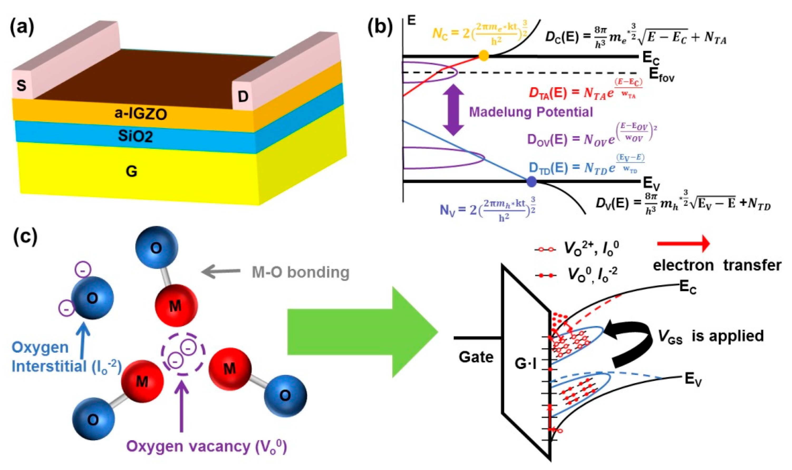
Figure 1a displays a schematic of the structure of a-IGZO-based bottom gate (BG)-top contact (TC) TFT. The gate (G), gate insulator (GI), active layer, and source (S) and drain (D) materials are n-polysilicon, SiO
2, a-IGZO, and aluminum, respectively. The GI and a-IGZO active layer have a thickness of 100 and 20 nm, respectively. The a-IGZO width (W) and length (L) are 180 and 30 µm.
Figure 1b schematically illustrates the sub-gap DOS distribution in relation to
mr* in a-IGZO TFTs. Both
NTA and the conduction-band DOS (
DC (
E)), and tail donor-like edge traps density (
NTD) and valence-band DOS (
DV (
E)) are theoretically continuous at boundary condition (BC) [
16]. In addition, the Madelung potential could lead to a metastable condition. Therefore,
VO could form near the conduction band (
EC) when the device is operated.
Figure 1c presents a bonding model and the schematic of the energy band diagram in the a-IGZO TFT. When the gate voltage is applied, electrons are generated and operated to accumulation mode by
VO and oxygen interstitials (
IO−2) because of the Madelung potential and peroxide model [
5,
7].
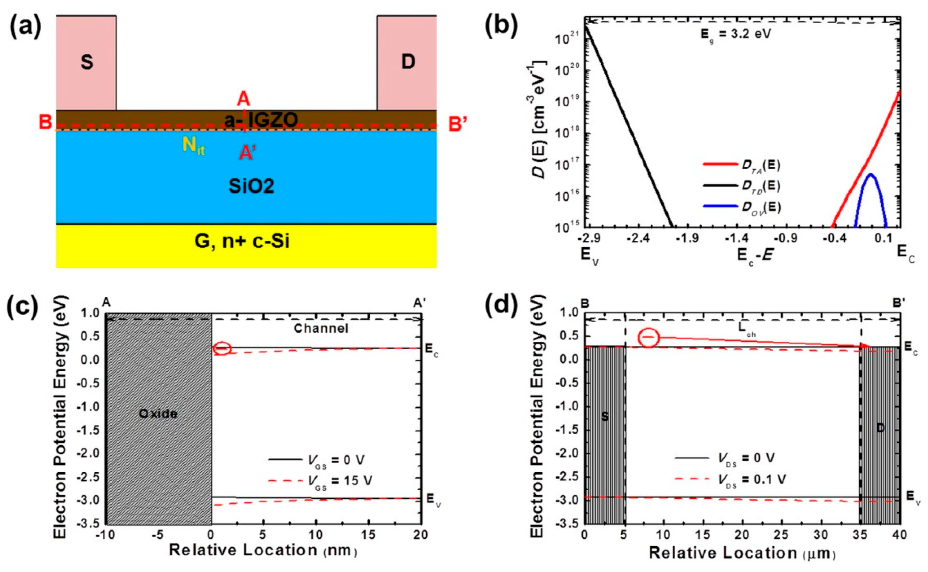
Figure 2a shows a cross-sectional view of the a-IGZO-based BC-TG TFT. We applied the interface traps model of Heiman [
17,
18].
Figure 2b shows the sub-gap DOS distribution designed to match the RF-sputtered a-IGZO TFTs in terms of their electrical characteristics (RF sub-gap DOS) via sub-gap DOS engineering mechanism [
13,
15].
The total acceptor-like DOS (
DTA (
E)), total donor-like DOS (
DTD (
E)), and
VO DOS (
DOV (
E)) have the properties of acceptor-like traps, donor-like traps, and
DOV (
E), respectively. In practice, both
NTA and
NTD in the sub-gap DOS increase because of the presence of process stress and hydrogen defect states [
5,
8]. In this study, the RF sub-gap DOS design parameters were selected to match the RF-sputtered transfer characteristics of the a-IGZO TFTs as presented below in
Table 1.
Figure 2c,d present an energy band diagram of the a-IGZO TFT with an A to A′ vertical cutline and a B to B′ lateral cutline. This illustration can not only explain the mechanism of field-effect TFTs, but also can be used to predict the electron distribution when the device operates according to Poisson’s Equation from Labels (3) to (6):
where
is the a-IGZO dielectric constant set at 10 in this study,
is the vacuum permittivity,
F is the electric field,
q is the elementary charge,
WD is the depletion width, and
x is the relative location. The energy band analysis could observe the effect of traps through the variation of energy when an electron is working.
Figure 3 shows the relationship of
mr* to the design parameters:
NTA,
NTD, thermal velocity (
vt), the lifetime related to trap site (
) at the
NOV (donor-like edge traps density of
DOV (
E)), and the hall mobility (
μ0). These variables were calculated using formulas from Labels (7) to (10), respectively [
18,
19]. At an
me* of 0.34 and an
mh* of 21 m
o [
5,
13], the following design parameters were obtained: a
NTA of 4.97 × 10
18 cm
−3eV
−1, a
NTD of 2.41 × 10
21 cm
−3eV
−1, a
vt of 2 × 10
7 cms
−1, a
of 10 ns, a
of 2 ns, and a
μ0 of 22 cm
2V
−1s
−1. As a result, we can completely obtain the transfer characteristics of the RF-sputtered a-IGZO BG-TC TFTs (
Table 2).
in the above Equations,
k is the Boltzmann constant, and
t is room temperature of 300 K.
cn,p is the capture cross-section of electron and hole,
NT (
E) is the trap-DOS in the active layer, and
h is the Planck constant (2πђ).
We assumed that
CAn,
CAh,
CDh, and
CDn were 1 × 10
−14, 1 × 10
−16, 1 × 10
−16, and 1 × 10
−14 cm
2, respectively, since the acceptor-like traps are negatively charged when occupied by an electron, and the donor-like traps are positively charged when emptied. We also assume a fully ionized
DOV (
E) at the metastable condition. Thus, the electron concentration was calculated to be 1 × 10
17 cm
−3 and (
EC −
Ef) is calculated to be 0.1 eV using Equation (9):
The interface traps were modeled with the Heiman model because the electrical mechanisms between the GI and semiconductor layer are better expressed when the transient time is taken into consideration during device operation. The Heiman interface mechanism could be obtained from the following equations:
where
Nit is the effective interface traps density and
d is the interface traps density depth between a-IGZO and GI. For a more accurate simulation, we used Shockley–Read–Hall (SRH) recombination with trap-assisted tunneling [
18,
20]:
where
Erh is the hole tunneling range,
Ern is the electron tunneling range, and
ET is the trap energy level.
3. Results and Discussion
Figure 4a shows the drain current-gate voltage (
IDS −
VGS) transfer characteristics at the RF sub-gap DOS with the variation of
me* in the linear and saturation regions. As
me* increased up to 0.44 m
o,
μfe and
Ion in the linear region fall to 10.6 and 2.7 µA, respectively. In order to analyze the effect of only changing
me*, we extracted a vertical energy band diagram at
VGS = 15 and
VDS = 0.1 V using the simulation tools as shown in
Figure 4b. As
me* changed from 0.24 to 0.44 m
o, the electron potential energy also increases from −0.067 to −0.049 eV. This meant that high
me* electrons were more easily captured and hardly emitted when compared to low
me* electrons. This was due to the negative charge of acceptor-like traps when holding the electrons, which could be explained using the Poisson’s Equation. Therefore, the relationship between
me* and
NTA is expressed as:
The et defines the probability that the electrons are trapped by NTA, and ee defines the probability that the electrons escape NTA. It was utilized to study the effect of me* through energy band analysis.
However, it is necessary for BC to consider the variation of
NTA by
me*. as the
NTA would cause sub-gap scattering. The sub-gap scattering could be reinterpreted by the following Equations [
13,
18]:
In the above equations,
denotes phonon scattering due to lattice vibrations,
represents surface scattering due to interface traps,
shows sub-gap scattering, the cubic is
DOV (
E) and
DTA (
E) per cubic centimeter, and a and b are experimental coefficients. Therefore, a-IGZO TFT could reinterpret the sub-gap scattering mechanism.
Figure 4c shows that, by changing
me*,
NTA is theoretically is affected. The
NTA was increased from 2.95 × 10
18 to 7.32 × 10
18 cm
−3eV
−1 when the
me* changed from 0.24 to 0.44 m
o.
WTA is not related to
mr* but rather related to amorphous randomness [
9,
11], and N
GA (
E) is not related to
mr* but rather deep traps density [
4,
8]. Thus, these values were maintained. Therefore, in order to accurately interpret the effect of electrical characteristics on
mr*, W
TA and N
GA (
E) should maintain their values in this paper. As a result, we observed a high variation of transfer curve under the
Vth region at the BC sub-gap DOS as shown in
Figure 4d. In order to obtain more detailed electrical performance trends, we used the
gm extraction method as below Equation [
3,
5]:
Thus,
μfe and
Vth can be obtained using the following
gm extraction equation:
The Cox denotes the SiO2 capacitance.
Figure 5a shows
µfe by changing
me* at the RF and BC sub-gap DOS distributions in the linear and saturation regions. As the
me* increased from 0.24 to 0.44 m
o,
µfe decreased from 16.4 to 10.6 cm
2V
−1s
−1 in the linear region, and from 17.1 to 10.8 cm
2V
−1s
−1 in the saturation region at the RF sub-gap DOS distribution. At the BC sub-gap DOS distribution, as the
me* increased from 0.24 to 0.44 m
o,
µfe also decreased from 18.5 to 11.7 cm
2V
−1s
−1 in the linear region, and from 19.7 to 12.1 cm
2V
−1s
−1 in the saturation region. It was found that the BC sub-gap DOS distribution exhibited higher
µfe than the RF sub-gap DOS distribution because of relatively high
NTA.
Figure 5b shows the variation of
Ion with
me* at the RF and BC sub-gap DOS distributions in the linear and saturation regions. As
me* increased from 0.24 to 0.44 m
o,
Ion decreased from 4.0 to 2.7 µA in the linear region and from 0.23 to 0.16 mA in the saturation region at the RF sub-gap DOS distribution. At the BC sub-gap DOS distribution, as
me* increased,
Ion also decreased from 5.3 to 3.2 µA in the linear region, and from 0.36 to 0.21 mA in the saturation region. It was found that the BC sub-gap DOS distribution exhibited higher
Ion than RF sub-gap DOS distribution also because of the relatively high
NTA. The high
NTA distribution in the a-IGZO TFTs was caused by the increasing probability of capture electron and sub-gap scattering.
Figure 5c shows the change in
Vth with the variation of
me* at the RF and BC sub-gap DOS distributions in the linear and saturation regions. As
me* increased from 0.24 to 0.44 m
o,
Vth decreased from 3.4 to 2.9 V in the linear region, and from 3.3 to 2.6 V in the saturation region at the RF sub-gap DOS distribution. Unexpectedly, the
Vth decreased in the transfer curve at the RF sub-gap DOS distribution, because the
x-axis intersection had negative shifted with decreasing slope, as evident from the
gm extraction equation. However, intrinsic
Vth would have a slight increase as noticed through energy band analysis. At the BC sub-gap DOS distribution, as
NTA increases from 2.95 × 10
18 to 7.32 × 10
18 cm
−3eV
−1 by varying
me* from 0.24 to 0.44 m
o,
Vth increased from 0.7 to 1.5 V in the linear region, and from 0.7 to 1.3 V in the saturation region. It was found that
NTA affected
Vth more than
me*. This could be utilized to predict the practical tendency of
Vth through optimizing
me*.
To illustrate this trend, we reinterpreted the conductivity mechanism [
21]. It can be expressed to drift drain current density (
Jn,drift) as
Thus, the conductivity is
It is hypothesized that the observed positive shift in
Vth at the BC sub-gap DOS was because of the low conductivity, which caused difficulty in channel formation through the electron capture by
NTA. To understand it in more detail,
Figure 5d shows the mechanism of multiple trapping and release (MTR) [
22], sub-gap scattering, and low conductivity effect of
me*. Therefore,
me* is a very important parameter because it affects
NTA, and has a major influence on the electrical performances in a-IGZO TFT. In addition, we would expect greater improvements in device performance to arise from appropriate
me* design and sub-gap engineering compared with conventional a-IGZO TFTs.

 ,
, 


