Abstract
CVCF (constant voltage, constant frequency) inverters are electronic devices used to supply AC loads from DC storage elements such as batteries or photovoltaic cells. These devices are used to feed different kinds of loads; this uncertainty requires that the controller fulfills robust stability conditions while keeping required performance. To address this, a robust design is proposed based on resonant control to track a pure sinusoidal voltage signal and to reject the most common harmonic signals in a wide range of loads. The design is based on the definition of performance bounds in error signal and weighting functions for covering most uncertainty ranges in loads. Experimentally, the controller achieves high-quality output voltage signal with a total harmonic distortion less than 2%.
1. Introduction
A VSI (voltage source inverter) consists of a DC–AC converter used to feed loads or generate energy support in the transportation or distribution stages of a power system grid. In this case, the CVCF (constant voltage, constant frequency) inverters are considered because the amplitude and frequency of the output voltage never changes along the time. The main objective of the control techniques is to maintain optimal conditions over the output voltage signal in parameters such as RMS (root mean square) value and THD (total harmonic distortion) index. The most common techniques used for CVCF applications are Repetitive control [1,2] and resonant control [3,4,5,6], where the designs are intended to achieve robustness over different loads, to reach adequate output voltage signal results, and to guarantee grid current low distortion. The resonant control, which is based on internal model principle (IMP), uses finite harmonic components. In comparison with the repetitive control, which demonstrates better performance in tracking, the resonant control technique achieves a better transient response and less order resulting compensator [7]. For that reason, the resonant control offers a suited option to design a robust controller in CVCF inverter applications.
There are different methods to design a resonant control for CVCF inverters [8,9,10]. These strategies try to optimize the closed-loop phase and gain margins, but they rely on the nominal plant model for this. Therefore, the main drawback of these designs is that the robustness margins are highly affected when different loads are connected to the CVCF inverter. Connecting and moving different kinds of loads (linear or nonlinear) generate large dynamic changes in the system. As a consequence, the plant model uncertainty increases dramatically. This might affect mainly the performance (tracking the sinusoidal reference without distortion) and robust stability (some loads might make the closed-loop system unstable).
Control theory offers options to address this problem, one of these options is the robust control theory, and the special case of design [11]. This technique combined with resonant control is used to improve the robustness of the system in a CVCF inverter. The proposal uses a single resonator on the current signal fundamental frequency, modeled as an error signal weighting function, and uses procedure to synthesize an optimal controller. The proposal presented in [12] tries to design a robust controller with multiple resonators on the output voltage signal. Subsequently, an augmented plant with uncertain load consideration is defined, based on an internal model of multiple resonators and admittance bounds. They also use linear matrix inequalities (LMI) to obtain a robust controller achieving until 2.7% of THD over a nonlinear load.
The present work proposes a structured and systematic approach for the design of a robust controller based on resonant control. The load uncertainty is considered in a direct form and the performance bounds are defined in the design process with weighting transfer functions on the error and control signals. Consequently, a two input and single output controller is proposed. The inputs are the error signal, , and the output voltage, , because these variables will allow a greater design flexibility. The proposed control system demonstrates in experimental results that a THD lower than 2% can be achieved in linear and nonlinear loads.
The study in [11] is clearly related to the proposal presented here, but it is not directly comparable because their converter approach is the output current control for grid coupled inverters and the single resonator design does not provide the rejection of harmonic signals. Additionally, the aforementioned study presents the load uncertainty as a multiplicative model, which is an indirect way to characterize the uncertain loads in the system.
Proposed scheme presents two key differences in comparison with [12]: here an optimization problem based on the classic design is presented such that the solution scheme is simpler than the LMI formulation in [12]. Also, the controller gains design in [12] is calculated based on the multiple resonators structure embedded in the Augmented Plant formulation, while our proposal uses the multiple resonator design on the error weighting function. It allows a convenient controller frequency response shaping based on the desired robust stability and performance. Therefore, the main contributions this work are:
- The consideration of the load connected to the CVCF inverter as a direct uncertainty without using standard uncertainty multiplicative or additive models
- A systematic design of weighting functions into a -mixed sensitivity classic structure
- This design does not require the use of new approaches to optimization problems with LMI formulation
- This design uses multiple resonators for reference tracking and harmonics rejection.
This paper is organized as follows: In Section 2 a system model and mathematical layout for the CVCF inverter with a LC filter is described. In Section 3 the robust control system design is explained using a mathematical problem statement with the systematic design of the weighting functions used and the augmented plant definition, to the robust stability analysis and description of the synthesized controller. In Section 4 an experimental validation is performed through the consideration of several linear and nonlinear loads applied to a digitally controlled CVCF inverter with the robust design obtained in the previous section. Finally, in Section 5 some conclusions of this research are presented based on the experimental analysis of results.
2. System Model Description
Figure 1 shows the scheme of a single-phase full bridge DC–AC converter. It is composed of a DC-link voltage described by , four power transistors IGBT (isolated gate bipolar transistor) that are switched in pair through a duty cycle d, an LC filter with the system dynamics (the inductance current and the capacitor voltage) and an uncertain load that generates a current from the output inverter voltage . It is necessary to operate in closed-loop form to avoid the voltage, , distortion caused by the load and being able to compensate the pulse width modulator (PWM) dead time.
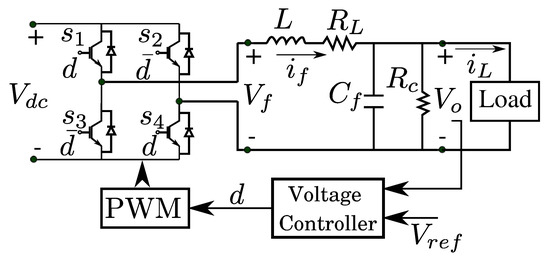
Figure 1.
CVCF inverter with uncertain load circuit diagram.
From Kirchhoff’s voltage law, the state and output equations of an averaged behavior can be extracted, as shown in Equations (1) and (2), respectively. The mathematical model can be depicted in different ways considering more or fewer circuit elements and dynamics as shown in [13,14]. In this proposal, the system states are , and correspond to the inductor current and capacitor voltage, respectively. is the input filter voltage that contains a time delay of seconds given by the PWM generator. The parameter L is the filter inductor and is the filter capacitor. and are the parasitic resistances of the inductor and capacitor, respectively. Additionally, the relationship is given, where is the DC bus voltage. The average of the switching function is defined in the interval (0, 1) and corresponds to the duty cycle imposed in the transistor gates. The reference sinusoidal voltage is depicted by .
where
Now, for design convenience, a transfer function form of the system is proposed in order to separate the control input and the disturbance input described by , as depicted in Figure 2. This Laplace domain model is especially useful to represent the uncertain load without any indirect uncertainty model, as considered in [12,15].
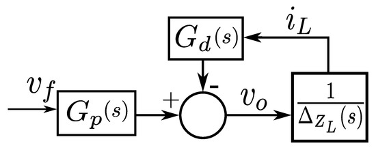
Figure 2.
Reduced block diagram for CVCF inverter with decoupled inputs.
According to Figure 2, Equations (3)–(5) depict the transfer functions and the relationship between the system inputs and outputs, where is the converter transfer function with its corresponding input delay, the function models how the load current affects the output voltage and the related uncertainty is referred as the parameter for any linear load. However, for nonlinear loads, it is not possible to represent the impedance as a Laplace transfer function and instead there is a completely uncertain system with unknown dynamics.
The uncertain load is represented in a direct way because the real relationship between the output voltage and the load current is featured as shown in Figure 2. With this fact, it is not necessary the use of standard plant uncertainty models such as multiplicative or additive [16].
For controller implementation objectives, the Equations (6) and (7) show a discrete-time model for the plant that is obtained from Equations (4) and (5) based on the Transform and the zero-order hold method, with as the constant sampling time of the discrete system.
3. Robust Control System Design
The control objective is to provide a sinusoidal voltage output with low distortion. It implies a THD index lower than 5%, which is a value accepted in common power quality standards such as IEEE Std-519 [17] and IEEE Std-1547 [18]. This bound must be achieved despite the kind and value of the load placed in the output of the CVCF inverter.
The load directly affects the system dynamics and injects harmonic signals, especially in the case of nonlinear loads. In fact, the load is unknown in real applications. Therefore, a sufficiently robust controller needs to be considered to deal with the model system uncertainty. Moreover, the controller must provide the rejection of periodic disturbances originated by the load.
In this way, an design based on resonant control is proposed for voltage loop control of the CVCF inverter. The resonant controller-like response of the compensator will guarantee the rejection of harmonic signal disturbances and sinusoidal voltage signal reference tracking (robust performance). tuning method will ensure the robustness needed to maintain the stability against a wide range of load variations (robust stability). Additionally, the optimization approach is focused on the control system design considering the possible uncertainties of the plant in its parameters or non-modeled dynamics [19].
The design begins with the generalized plant definition based on weighting transfer functions which will set the control design criteria [20]. The controller synthesis results from an optimization problem that consists of the infinity norm minimization from inputs to outputs of the generalized plant. A two-degree of freedom controller as depicted in Figure 3 is proposed. The condition of two degrees of freedom permits enough design flexibility for reaching robust stability and performance.
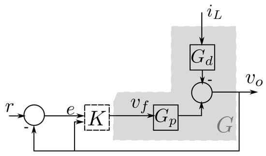
Figure 3.
Control system block diagram proposed for CVCF inverter.
The augmented plant is defined by the weighting functions assigned to the error signal depicted by , the filter input voltage or control signal described by , while the load uncertainty is expressed as a frequency dependent weighting function and an unstructured uncertainty , with , such that the load uncertainty satisfies [21]. Those weighting functions are discrete-time transfer functions that are chosen based on determined performance criteria. Figure 4 shows the representation of the generalized plant as a white box where the weighting transfer functions are applied in the chosen signals. The controller is dismissed temporally because it will be the design result. The load will be considered to be an uncertain system with any impedance magnitude, therefore, the weighting function is designed to cover the longest possible interval of load variations.
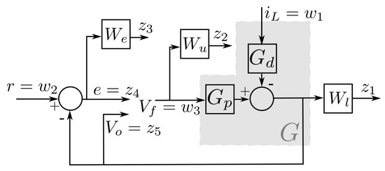
Figure 4.
Generalized plant as a white box model.
The generalized plant has an input signal vector which is composed of the load current, the reference and control signals, i.e., (k is the discrete variable in time domain), while the output vector comprises the outputs of weighting transfer functions depicted as , , , the error signal and the inverter output voltage, i.e., . These representations generate a MIMO (Multi Input Multi Output) system that will have a controller with inputs and output . Figure 5 shows the resulting closed-loop system structure, with as the generalized plant, as the controller discrete transfer function and the plant uncertainty. This uncertainty , in our case, is due to the unknown loads that are connected to the VSI. The main objective of the proposed optimization is to synthesize a controller to provide robust stability to the closed-loop system shown in Figure 5 considering the uncertainty [16].
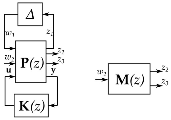
Figure 5.
Proposed closed loop for the design.
According to the approach explained in Figure 4, the generalized plant results in Equation (8). The MIMO rule is used to find input-output relationships [16] and therefore, the transfer functions that integrate . The optimization problem is defined by synthesizing the controller that minimizes the infinity norm of .
Equation (9) shows the optimization problem where corresponds to the minimum norm achieved when a controller in the closed loop is used, as illustrated in Figure 5. The synthesis finds a controller that guarantees a value less than 1 or the robust stability condition accomplishment. It must be achieved for the three performance indexes that are closely related to a S-KS or mixed sensitivity problem, as developed in [16,21]:
where the transfer function , the local sensitivity function related to the closed loop between and called and the total sensibility function of the closed loop . The weighting functions perform an important role in the controller synthesis and their selection will generate a more or less robust controller for the CVCF inverter. While takes a lower value, the closed-loop will support higher uncertainty ranges. If the controller generates a closed-loop norm close to 1, stability could be compromised for some range of load impedances. Even more, if Equation (9) is achieved and considering that , the robust stability of the closed-loop system is guaranteed [16,19].
3.1. Weighting Functions Design
The weighting functions design is based on the desired performance in the chosen signals. Their main objective is to penalize the signals in the selected frequencies. In this proposal, the error signal must be small in the fundamental frequency and its multiples. This condition leads to high-quality tracking and disturbance rejection characteristics. Additionally, the control signal must be weighted to avoid saturation in actuators and high frequency response in the controller. The output signal acquires a special treatment with a function that covers a wide range of load uncertainties based on the impedance magnitude parameter.
3.1.1. Error Weighting Function
The error weighting function depicted as is designed such that the difference between the reference signal and the output voltage of the CVCF inverter achieves a very little value at desired frequencies. Therefore, the incorporation of a sinusoidal signal representation in the controller is needed. This process is reached using a resonator [7] and is defined in Equation (10) as a discrete-time domain transfer function. The desired resonator frequency is , is a positive gain that determines the resonator response time, is the phase shift of the resonant element at frequency , and is the sampling time.
However, pure resonant controllers are not considered because the weighting function must be stable. Therefore, a very little damping factor (that limits the resonator gain) is incorporated in the design for preventing the cancellation. The final expression for the “damped” resonator is given in Equation (11) where corresponds to the damping factor, , , and the variable . This equation is obtained from the step invariance method of discretization of analog controllers illustrated in [22], based on the analog transfer function of the damped resonator which corresponds to .
To achieve reference tracking and harmonic rejection, a multiple resonator sum at desired sinusoidal frequencies is proposed as shown in Equation (13). This equation depicts the general result of the weighting error function, where l is the resonant element index and m is the number of resonators considered. In this case, the most common frequencies given by linear and nonlinear loads are chosen. Specifically, the third, fifth, seventh, ninth, eleventh and fifteenth harmonics are considered and defined by the angular frequencies given in Equation (12). The harmonic number is n and is the fundamental frequency that corresponds to the Latin-American power line frequency at 60 Hz.
The tuning procedure seeks the gains and the phase shifts values to reach the desired performance with enough robustness margin controller. In this case, as the design procedure gives the required robustness, the phase shifts will correspond to the phase value of the plant at frequency . Each resonant element gain is given to provide the best possible performance. While takes a high value, the tracking (at fundamental frequency) or rejection (at harmonics) will have a better effect, but the stability margin is affected when the variable comes very high. Therefore, the numerical values obtained for the tuned damped resonant elements shown in Equation (11) are: , , , s, and the other parameters of the equation will depend on those values.
The number of resonant elements must be considered in the error weighting function design because using a high p value might yield a controller of very high order with a complex implementation. It is important to notice that due to the waterbed effect, as illustrated in [23], it is not possible to attenuate the error signal for all frequencies.
The error weighting function frequency response is shown in Figure 6, where it is expected that the error has the higher attenuation at fundamental and harmonic frequencies. It will reflect a high gain in the controller at those frequencies, assuring the initial objectives accomplishment.
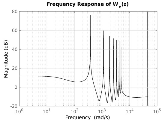
Figure 6.
Frequency response of the proposed error weighting function, .
3.1.2. Control Signal Weighting Function
A weighting function of low-pass filter shape is proposed. The principal objective of this weighting function is limiting the amplification of the control signal at high frequencies. This is mainly due to the tendency of the compensators to adopt the inverse frequency response of the plant. The weighting function for control signal is defined in Equation (14) while the frequency response is depicted by Figure 7. This function allows the reaching of a controller gain sufficiently less than 7 dB in high frequency ranges and less than dB in low ones so that low penalization of the control signal expected spectra is achieved.
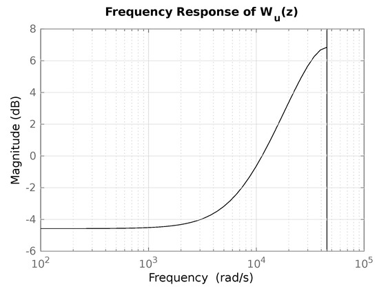
Figure 7.
Frequency response of the proposed control weighting function, .
3.1.3. Output Signal Weighting Function
The output signal weighting function tries to cover the most quantity of load uncertainties based on their magnitude frequency response. As shown in Figure 2, the relation between and is , which means that should corresponds to the frequency response of the load admittance. In addition, as the desired inverter performance consists of feeding the most quantity of possible loads, the admittance must be as large as possible throughout the frequency range.
Furthermore, as the transfer function is extracted from the input to , corresponds to the converter output impedance and it has to be the smallest possible for all frequencies to guarantee the maximal power transfer to the load.
Therefore, the weighting function depicted by must be the greatest possible in all the frequency range. This fact forces to execute some iterative experimental validation to obtain an adequate transfer function for weighting the load, after which it took the form presented in Figure 8 with some frequency responses of inductive linear loads covered by the weighting function, from an admittance value of 0.1 in low frequencies to 0.09 in high ones. In this case, the weighting function takes the expression depicted in Equation (15).
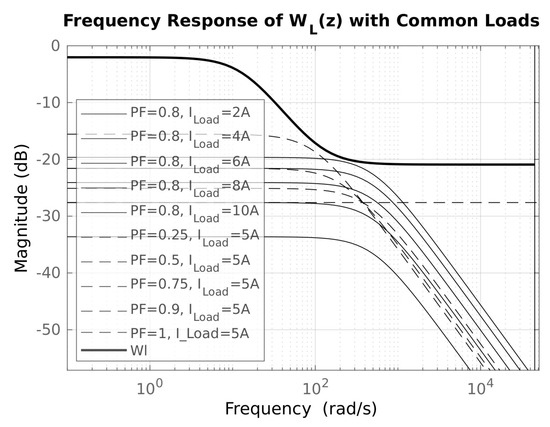
Figure 8.
Frequency response of the proposed output weighting function covering some linear inductive loads, .
3.2. Controller Syntesis
Based on the generalized plant, the controller synthesis by design is performed, where the optimization problem described in Equation (9) is solved. A 20-second order controller is obtained. Its frequency response is illustrated in Figure 9 for each component of the controller, where handles the harmonics rejection and has effects on the transient and affords flexibility for the design accomplishment. The general discrete transfer function as zero-pole form is shown in Equation (16), where , and are the poles and zeros of the controller respectively. The numerical values are depicted in Table 1. As expected, the controller has a high gain at the fundamental frequency and its harmonics.
where: with 1, 2 and ; .
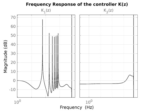
Figure 9.
Bode diagram for synthetized controller.

Table 1.
Poles and zeros of the controller discrete transfer function.
The controller poles and zeros are shown in Figure 10 where the common resonant poles for are located in the limit of the unit circle to guarantee the error magnitude minimization at desired frequencies in steady-state regimen. For the case of the poles and zeros are very close located such that all the resonant poles can be cancelled by their zero-pairs. This cancellation causes that the closed-loop system response capabilities can improve in terms of the remaining dominant poles with real part close to zero.
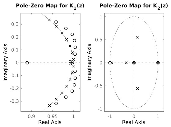
Figure 10.
Poles and zeros location for the synthesized controller.
Moreover, this controller does not permit order reduction because the particular form of the controller frequency response would be lost and the robust performance or even the closed-loop stability would not be assured.
3.3. Stability and Robustness Analysis
Once the controller has been obtained, the robustness analysis compares the performance bounds (inverse multiplicative of the weighting transfer functions) and the specific sensitivity closed-loop transfer functions. Those transfer functions can be extracted from Equation (9) by dividing the robustness index into the weighting function associated with it.
In any case, for testing the performance for output impedance, the transfer function with input and output is compared with the bound . This case is presented in Figure 11 and the desired performance is demonstrated since the frequency response magnitude of the output impedance never surpasses the performance bound [19].
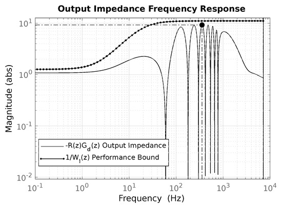
Figure 11.
Performance of the output impedance for closed-loop design.
The peak gain of the output impedance is the minimum value of the load magnitude supportable by the CVCF inverter. In this case, the bound was fixed to 10 and the synthesized controller achieved a minimum value of the load magnitude of 9.3 . Load impedances lower than the peak value do not assure robust stability in the closed-loop system.
Additionally, the robustness of the closed-loop design for the performance bound is tested in the error signal. As in the previous case, the sensitivity function (transfer function from to ) is evaluated with the bound given by the inverse multiplicative of the weighting function . The comparison result is shown in Figure 12, where the error signal takes the lowest magnitude in key frequencies, as expected. This demonstrates the capabilities of the controller to track the sinusoidal reference and reject the selected harmonics, according to the design criteria. The design also shows that the frequency magnitude peak of the sensitivity function reaches values lower or equal than 6 dB, which prevents considerable noise effects and preserves a good enough modulus margin. In the same figure, the performance bound given by has an infinity norm less or equal than 10 (or 20 dB) because the directly related error weighting function would not fulfill the stability requirement.
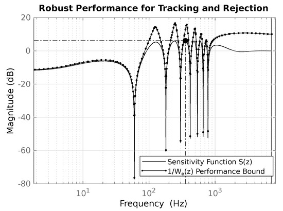
Figure 12.
Error robust performance for closed-loop design.
The difference between the nominal behavior of the control system and the performance bounds shows that the designed controller can deal with the important parametric uncertainties into the plant. The infinity norm achieved by the design with the performance index related to the error signal reaches a value of . This value means that the controller can support until of nominal plant variation before the error performance bound be broken.
For the case of the control signal, the comparison of the performance bound and the related relation between the control signal and the reference signal (saturation analysis) is shown in Figure 13 depicting that high frequency signals given by disturbances and switching effects would be attenuated by the control action, while the interest frequency intervals (fundamental frequency and harmonics) will have an appropriate amplification so that the robust stability and performance can be achieved.
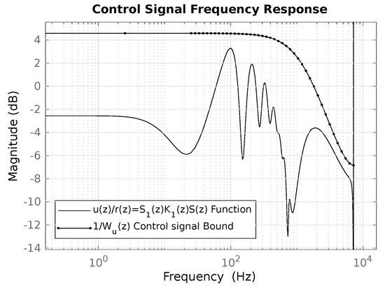
Figure 13.
Performance for control signal.
Accordingly, the tuning process and the method for achieving a satisfactory controller is shown in Figure 14. The method starts with the generalized plant definition through the selection of both the key signals to be weighted and the control architecture. In this case, as shown, the error, control, and output signals are chosen for weighting, while a two-degree of freedom control architecture is proposed. After that, through multivariable block diagram operations [16], the generalized plant is defined as shown in Equation (8). Later, with the total number p and per element frequency , the selection of resonant components is performed and Equation (13) helps to define them. Next, the weighting functions definitions on the chosen signals are implemented applying the resonant components statement in and adequate functions for control signal and load uncertainty. The controller synthesis is performed through the formulation (with the robustness index statement of Equation (9)) and solution of the optimization problem. Then, the synthesized controller is verified through validation of the robustness index that most satisfy the small gain theorem [21], the harmonic rejection objectives (through the THD index according to the standards), and the transient performance so that neither overshoots nor high response times take place. If either robustness index condition or transient performance are not satisfied, the weighting functions definitions must be adjusted. In another case, the selection of resonant controllers must be modified (through tuning the resonators gains, phase shift values or total number of resonant components) if the harmonic rejection performance condition is not satisfied.
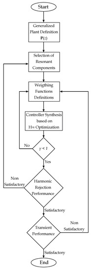
Figure 14.
Proposed method to achieve a satisfactory robust control system design.
4. Experimental Validation
The controller is implemented in a CVCF converter whose parameters are given in Table 2. The DC–AC Converter of reference Semikron SemiTeach® is composed of an IGBT bridge, a DC bus and a diode bridge rectifier. In this case, both the digital control sampling frequency and the switching frequency of 14.4 kHz is chosen, which is an integer multiple of the operating frequency of the inverter, Hz. Additionally, the control system is implemented in MATLAB XPC-Target, which is a rapid control prototyping platform [24]. The experimental setup with the digital control platform, the power stage, LC filters, and loads is shown in Figure 15.
Table 2.
CVCF (constant voltage, constant frequency) inverter parameters.
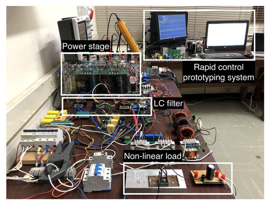
Figure 15.
Experimental setup for the robust control of the CVCF Inverter.
The loads chosen to test the CVCF inverter vary from linear to nonlinear nature with different magnitudes and a wide range of power factor. A pure resistive, high and low inductance RL, and nonlinear loads are considered. The linear loads are formed with a resistance of 12.8 with several inductors achieving different power factors. The nonlinear load is based on a diode rectifier with parallel RC output of values of 51.5 , and 680 F, respectively. Table 3 depicts the different kinds of loads tested in the converter and shows the THD index of the current signal obtained with these loads. Also, the power factor, the apparent power and the voltage THD reached by the control system in the CVCF converter are shown. This table is the result of a steady-state analysis and corresponds to a power quality testing. The reference control system signal is 110 with 60 Hz pure sinusoidal signal.
Table 3.
Experimental results and tests.
The results show that the robust control system can track the signal reference and rejecting the distorted current signal of the load with high performance and different power consumption in all cases.
The results shown in Table 3 for steady-state regimen are compiled in Figure 16, Figure 17, Figure 18, Figure 19 and Figure 20. Each figure has three illustrations that correspond to the closed-loop output voltage THD in the harmonic analyzer (upper left), load current THD (upper center), power analysis (upper right) and a detailed both voltage and current waveforms by oscilloscope (below).
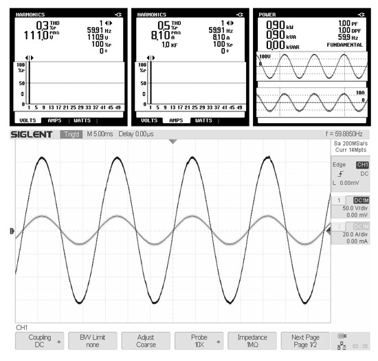
Figure 16.
Converter results for linear load with PF = 1.
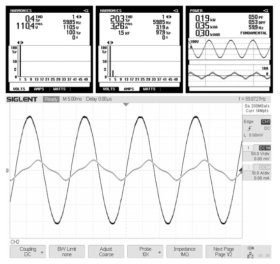
Figure 17.
Converter results for linear load with PF = 0.5.
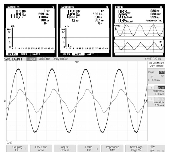
Figure 18.
Converter results for linear load with PF = 0.86.
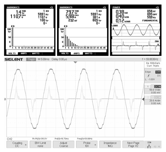
Figure 19.
Converter results for nonlinear load.
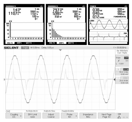
Figure 20.
Converter results for parallel linear and nonlinear load.
The proper results for linear loads are illustrated in Figure 16, Figure 17 and Figure 18 where different power factor loads are tested, giving different active and reactive power consumption. In all cases, despite the power factor and the low nonlinear effects by the inductors, which impose a third and a five current harmonic, the output voltage maintains a THD less than 0.5% thanks to the resonators tuned at those disturbance frequencies.
However, if the bound is not surpassed, the THD output voltage index will not have undesired percentages beyond 2%. Linear loads with inductive reactance as exposed in Figure 17 and Figure 18 show that the voltage distortion decreases when the power factor is reduced because the active power of the impedance becomes lower thanks to the current demand. Then, a good performance of the robust control is obtained since the total load impedance increases.
For nonlinear loads connection, the disturbance rejection is achieved for the current waveforms with high harmonic presence near of 80%. The greatest impact is caused by the nonlinear load connected to the converter because it has the most current harmonic distortion as shown in Figure 19, despite this event, the output voltage does not reach a THD more than 1% with an appreciable load power consumption.
In contrast, Figure 20 shows that the combination of a linear and nonlinear load, which the current waveform has less harmonics than in the last case, obtains a better rejection by the control system of the CVCF converter.
Regarding the transient regimen, parametric testing is not considered because each load generates a unique dynamical system change. Therefore, the dominant poles that define the transient regimen will vary with each experiment. Some results of the transient stage with load connection or disconnection are shown in this section.
When the nonlinear load is connected and the linear one enters too, as depicted in Figure 21, the voltage has a decrease in its amplitude that lasts until one cycle. But nevertheless, this effect is little harmful to the load because the voltage in transient stage does not decrease less than the ten percent of the peak value, which is within the allowable range for amplitude variations.
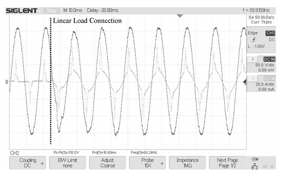
Figure 21.
Transient stage for linear load connection when the nonlinear one remains connected.
Also, the transient stage could be shown in the load transitions where disconnections events take place. Figure 22 shows the transient stage of the parallel connection of the linear load with the nonlinear one that is disconnected. In Figure 23 a linear load disconnection event (remaining the nonlinear one) is illustrated. The both cases show that the CVCF converter control system has a settling time less than two sinusoidal signal periods with non-harmful amplitude variations in the supplied voltage.
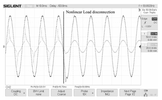
Figure 22.
Nonlinear load disconnection transient stage when linear load remains connected.
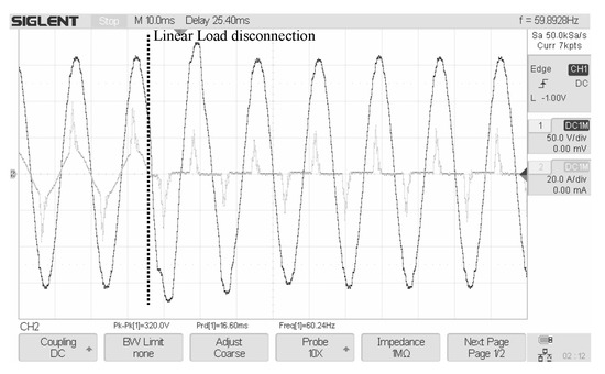
Figure 23.
Linear load disconnection transient stage when the nonlinear one remains connected.
5. Conclusions
A robust control design methodology for a CVCF inverter has been presented. This methodology combines the use of resonant elements that based on the internal model principle guarantees excellent steady-state behavior and to guarantee stability against load variations. The design shows that the converter has the capability to support a wide range of loads with different magnitudes that are greater than a determined minimum impedance value. The converter output voltage regulation was achieved with a THD less than 2% for a wide range of linear (with different power factor) and nonlinear loads. The synthesized compensator is obtained through an norm minimization procedure. The controller achieved the desired performance bounds throughout all the frequency range. The time domain performance shows a high-power quality signal, where a high harmonic rejection is achieved. The weighting functions are selected aimed at having good robustness bounds in the cases of the error and control signals. The output weighting function represents the maximum possible admittance for the frequency range, where the highest load uncertainty was included. The obtained controller satisfies all the robustness bounds, supports different kinds of loads and does not have critical transient stages or overshoots in load connection or load changing. The achieved robustness is demonstrated in the capability to maintain a high-quality voltage signal on load uncertainties.
Author Contributions
Conceptualization, H.B.-C. and G.A.R.; validation, H.B.-C. and G.A.R.; writing—original draft preparation, H.B.-C. and G.A.R.; writing–review and editing, R.C.-C.; supervision, R.C.-C. All authors have read and agreed to the published version of the manuscript.
Funding
This work was supported by Vicerrectoría de Investigación y Extensión, Facultad de Ingeniería at Universidad Nacional de Colombia on the Project ID. QUIPU: 201010028222 through the call “Convocatoria Nacional para el Apoyo al Desarrollo de Tesis de Posgrado o de Trabajos Finales de Especialidades en el Área de la Salud, de la Universidad Nacional de Colombia 2017-2018”. This work has been partially funded by the Spanish national project DOVELAR ref. RTI2018-096001-B-C32 (MCIU/AEI/FEDER, UE). This work is supported by the Spanish State Research Agency through the María de Maeztu Seal of Excellence to IRI (MDM-2016-0656). This work is partially funded by AGAUR of Generalitat de Catalunya through the Advanced Control Systems (SAC) group grant (2017 SGR 482).
Conflicts of Interest
The authors declare no conflict of interest and the funders had no role in the design of the study; in the collection, analyses, or interpretation of data; in the writing of the manuscript, or in the decision to publish the results.
References
- Astrada, J.; De Angelo, C. Reduction of the output impedance in single phase inverters for UPS combining conventional multi-loop and plug-in repetitive control. Rev. Iberoam. De Automática E Informática Ind. 2019, 16, 391–402. [Google Scholar] [CrossRef]
- Ramos Fuentes, G.A.; Isaza Ruget, R.; Costa-Castelló, R. Robust repetitive control of power inverters for standalone operation in DG systems. IEEE Trans. Energy Convers. 2019. [Google Scholar] [CrossRef]
- Sreekumar, P.; Danthakani, R.; Veettil, S.P. Implementation of proportional-resonant controller in an autonomous distributed generation unit. In Proceedings of the 2018 Advances in Science and Engineering Technology International Conferences (ASET), Abu Dhabi, United Arab Emirates, 6–7 Febuary 2018; pp. 1–5. [Google Scholar] [CrossRef]
- Husev, O.; Roncero-Clemente, C.; Makovenko, E.; Pimentel, S.P.; Vinnikov, D.; Martins, J. Optimization and Implementation of the Proportional-Resonant Controller for Grid-Connected Inverter with Significant Computation Delay. IEEE Trans. Ind. Electron. 2020, 67, 1201–1211. [Google Scholar] [CrossRef]
- Iftikhar, M.; Aamir, M.; Waqar, A.; Naila; Muslim, F.B.; Alam, I. Line-Interactive Transformerless Uninterruptible Power Supply (UPS) with a Fuel Cell as the Primary Source. Energies 2018, 11, 542. [Google Scholar] [CrossRef]
- Keiel, G.; Flores, J.V.; Lorenzini, C.; Pereira, L.F.A.; Salton, A.T. Affine discretization methods for the digital resonant control of uninterruptible power supplies. J. Frankl. Inst. 2019, 356, 8646–8664. [Google Scholar] [CrossRef]
- Dong, D.; Xu, D.; Xu, M. Experiment comparison of repetitive control and resonant control. In Proceedings of the 2016 IEEE 8th International Power Electronics and Motion Control Conference (IPEMC-ECCE Asia), Hefei, China, 22–26 May 2016; pp. 2150–2155. [Google Scholar] [CrossRef]
- Sato, Y.; Ishizuka, T.; Nezu, K.; Kataoka, T. A new control strategy for voltage-type PWM rectifiers to realize zero steady-state control error in input current. IEEE Trans. Ind. Appl. 1998, 34, 480–486. [Google Scholar] [CrossRef]
- Fukuda, S.; Yoda, T. A Novel Current-Tracking Method for Active Filters Based on a Sinusoidal Internal Model. IEEE Trans. Ind. Appl. 2001, 37, 888–895. [Google Scholar] [CrossRef]
- Hu, W.; Ma, W.; Liu, C. A novel AC PI controller and its applications on inverters. In Proceedings of the 2009 4th IEEE Conference on Industrial Electronics and Applications, Xi’an, China, 25–27 May 2009; pp. 2247–2251. [Google Scholar] [CrossRef]
- Wang, Y.; Wang, J.; Zeng, W.; Liu, H.; Chai, Y. H Infinity Robust Control of an LCL-Type Grid-Connected Inverter with Large-Scale Grid Impedance Perturbation. Energies 2018, 11, 57. [Google Scholar] [CrossRef]
- Pereira, L.F.A.; Flores, J.V.; Bonan, G.; Coutinho, D.F.; da Silva, J.M.G. Multiple Resonant Controllers for Uninterruptible Power Supplies-A Systematic Robust Control Design Approach. IEEE Trans. Ind. Electron. 2014, 61, 1528–1538. [Google Scholar] [CrossRef]
- Touati, A.; Abdelmounim, E.; Aboulfatah, M.; Abouloifa, A. Observation and control of a single-phase DC-AC converter with sliding mode. In Proceedings of the 2014 International Conference on Multimedia Computing and Systems (ICMCS), Marrakech, Morocco, 14–16 April 2014; pp. 1539–1544. [Google Scholar] [CrossRef]
- Hyun, D.Y.; Lim, C.S.; Kim, R.Y.; Hyun, D.S. Averaged modeling and control of a single-phase grid-connected two-stage inverter for battery application. In Proceedings of the IECON 2013—39th Annual Conference of the IEEE Industrial Electronics Society, Vienna, Austria, 10–13 November 2013; pp. 489–494. [Google Scholar] [CrossRef]
- Yang, S.; Cui, B.; Zhang, F.; Qian, Z. A Robust Repetitive Control Strategy for CVCF Inverters with Very Low Harmonic Distortion. In Proceedings of the APEC 07—Twenty-Second Annual IEEE Applied Power Electronics Conference and Exposition, Anaheim, CA, USA, 25 Febuary–1 March 2007; pp. 1673–1677. [Google Scholar] [CrossRef]
- Zhou, K.; Doyle, J.C. Essentials of Robust Control; Prentice Hall Modular Series for Eng; Prentice Hall: Upper Saddle River, NJ, USA, 1998. [Google Scholar]
- Halpin, S. Revisions to IEEE Standard 519-1992; 2005/2006 PES TD; IEEE: Piscataway, NJ, USA, 2006; pp. 1149–1151. [Google Scholar] [CrossRef]
- Zong, X.; Gray, P.A.; Lehn, P.W. New Metric Recommended for IEEE Standard 1547 to Limit Harmonics Injected Into Distorted Grids. IEEE Trans. Power Deliv. 2016, 31, 963–972. [Google Scholar] [CrossRef]
- Gu, D.W.; Petkov, P.H.; Konstantinov, M.M. Robust Control Design with MATLAB®. In Advanced Textbooks in Control and Signal Processing; Springer: London, UK, 2014. [Google Scholar]
- Sánchez-Peña, R.S.; Sznaier, M. Robust Systems Theory and Applications; Adaptive and Learning Systems for Signal Processing, Communications and Control Series; Wiley-Interscience: Hoboken, NJ, USA, 1998. [Google Scholar]
- Dullerud, G.E.; Paganini, F. A Course in Robust Control Theory. In Texts in Applied Mathematics; Springer: New York, NY, USA, 2000; Volume 36. [Google Scholar] [CrossRef]
- Chen, C.T. Analog and Digital Control System Design: Transfer-Function, State-Space, and Algebraic Methods; Oxford Series in Electrical and Computer Engineering; Saunders College Pub.: Philadelphia, PA, USA, 1993. [Google Scholar]
- Stein, G. Respect the unstable. IEEE Control Syst. 2003, 23, 12–25. [Google Scholar] [CrossRef]
- Chakirov, R.; Vagapov, Y. Rapid Control Prototyping Platform for the Design of Control Systems for Automotive Electromechanical Actuators. IFAC Proc. Vol. 2010, 43, 646–651. [Google Scholar] [CrossRef]


© 2020 by the authors. Licensee MDPI, Basel, Switzerland. This article is an open access article distributed under the terms and conditions of the Creative Commons Attribution (CC BY) license (http://creativecommons.org/licenses/by/4.0/).