Abstract
The operation and the design of organic solar cells with donor/acceptor heterojunction structure and exciton blocking layer is outlined and results of their initial development and assessment are reported. Under halogen lamp illumination with 100 mW/cm2 incident optical power density, the devices exhibits an open circuit voltage VOC = 0.45 V, a short circuit current density JSC between 2 and 2.5 mA/cm2 with a fill factor FF ≈ 50%, an external quantum efficiency (electrons/s over incident photons/s) EQE ≈ 5% and a power conversion efficiency of about 0.5%. Measurements of the photoelectrical characteristics with time are also reported, confirming that non encapsulated organic solar cells have limited stability in ambient atmosphere.
1. Introduction
Organic amorphous semiconductors in the form of polymers or oligomers (also called small molecules) have by now made their way in Electronics and Optoelectronics [1]. This is due to a simple and cheap chemical synthesis, not critical film deposition techniques even on flexible plastic substrates and, last but not the least, their unique and useful optoelectronic properties [2]. Organic thin films can be produced by several methods, such as high vacuum thermal evaporation for oligomers and spin-coating, drop-casting, screen printing, spray-coating and inkjet-printing usually for polymers. Applications include color displays based on organic light emitting diodes (OLEDs), paper (flexible) Electronics and, more recently, organic solar cells (SCs). Organic photovoltaics is indeed a very active research field, promising high efficiency, large area and low cost SCs [3,4]. Organic SCs with improved structures and materials, including bulk heterojunction [5] and perovskites [6], have reached power conversion efficiencies above 10% [7] but stability and lifetime is still an issue even with encapsulated devices [8]. In this contribution we report the design, initial development and assessment of donor (D)/acceptor (A) heterojunction SCs.
The D/A heterojunction is the archetypal structure of several organic SC structures, as first reported by Tang in 1986 [9]. Considering small molecule organic materials, photons absorption creates excitons, i.e., electron-hole pairs localized on the molecules and made stable by their Coulomb attractive force. These are also termed Frenkel excitons and can move by diffusion-driven hopping between nearest molecules under a concentration gradient. Their binding energy is quite high, even up to 1 eV, due to the low dielectric constant of the organic materials (εr ~ 3). For this reason, organic SCs are also called excitonic SCs.
Efficient organic SCs require the separation of the electron hole-pair (exciton dissociation) followed by charge transport and collection at the electrical contacts. Due to the high binding energy of the Frenkel excitons, direct dissociation by the internal electric field, although possible, has a very low probability, <10%. However, efficient excitons dissociation can be achieved at a heterojunction interface with proper energy levels offset for charge separation [9]. Frenkel excitons that reach the interface lose some energy and become charge transfer (CT) excitons, where electron and hole are now localized to neighboring and chemically different molecules on the two sides of the interface [9,10]. CT excitons are then easily split by the internal electric field allowing free electrons and holes to be collected at the electrodes.
Figure 1a shows the structure of an SC heterojunction made on a glass substrate, with a donor organic material (D) able to transport holes and an acceptor material (A) for electron transport. Figure 1b shows the open circuit band diagram of the D-A heterojunction SC, that is in flat band condition, where the energy levels are referenced to the vacuum level, taken as 0 eV. The energy level of the highest occupied molecular orbital (HOMO) is equivalent to the valence band edge in inorganic crystalline semiconductors. The energy level of the lowest unoccupied molecular orbital (LUMO) is equivalent to the conduction band edge. Consequently, the level offset at the D-A interface must be as indicated in Figure 1b, with the D material having electron affinity (EA) smaller than that of the A material, in order to easily release electrons (hence the term donor). As the A material accepts electrons (acceptor), this must have a ionization potential (IP) higher than that of the D material, for releasing holes to the D layer. The work functions of anode and cathode materials are also shown. The energy of the Frenkel exciton, generated by optical absorption, is lower than the HOMO-LUMO bangap by a value exactly equal to the exciton binding energy. The built-in voltage Vbi is given by the work function difference between cathode and anode materials and is ideally equal to the open circuit voltage VOC of the SC.
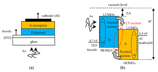
Figure 1.
(a) D-A SC structure; (b) Open circuit band diagram (flat band) with Frenkel excitons becoming CT excitons upon charge transfer at the D-A interface. On the A side there is the cathode metal electrode (usually Aluminum) and on the D side the transparent anode electrode (usually Indium Tin Oxide, ITO) to allow the transmission of the incident photons inside the SC.
A short circuited SC and its band diagram are shown in Figure 2a,b respectively. The band diagram with constant Fermi energy level helps to understand the photovoltaic effect in organic SCs. A photogenerated Frenkel exciton that reaches the D-A interface becomes a CT exciton upon charge transfer and this is then dissociated by the internal electric field. The free electrons are transferred to the A side and the free holes to the D side. Therefore, an external short circuit current density (JSC) flows through the external connection from anode to cathode. When a load is connected to the SC the external current density is smaller than JSC and the D-A heterojuntion is forward self-biased to a voltage less than Vbi. The SC operates as an electric power generator.
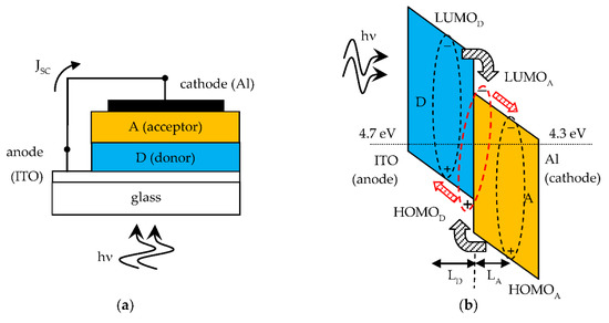
Figure 2.
(a) Short circuited SC; (b) Relevant band diagram showing the photovoltaic effect of the D-A solar cell. The exciton diffusion lengths LD and LA are indicated. Ideally the difference in work function energy levels between anode and cathode is VOC = Vbi of the solar cell.
As a final remark, the difference in energy between the LUMO of A and the HOMO of D must be smaller than the Frenkel exciton energy to ensure an ideally 100% probability of CT exciton formation at the D-A interface with subsequent charge separation by the internal electric field. If this requirement is not met, CT excitons cannot be formed and most Frenkel excitons reaching the interface will recombine and are lost, resulting in SC poor performance.
Organic materials have high optical absorption coefficients in the visible range (α ~ 105 cm−1 [1]) with corresponding absorption length L = 1/α of the order of hundreds of nm, which is indeed the typical thickness of organic SCs. Being this shorter than the wavelength of the photons, light reflection from the metal cathode creates a standing wave pattern in the device thickness with an associated distribution of photogenerated excitons. This pattern is actually made of a single antinode due to the small thickness of the absorbing layers, creating a concentration gradient. As a result, in general the excitons in the A layer diffuse toward the D-A interface and the metal cathode. Only excitons photogenerated within an exciton diffusion length from the D-A interface can reach this and be dissociated. The photoactive region of the organic SC is close to the D-A interface and is equal to the sum of exciton diffusion lengths, LD in D and LA in A, from the interface, as indicated in Figure 2b. Typically, organic materials have short exciton diffusion lengths, of the order of several nm [1]. But good D and A materials suitable for organic SCs have exciton diffusion length one order of magnitude higher. This is a relevant point, because the photoactive region is wider and consequently a higher power conversion efficiency can be expected.
Actually, the simple two-layer D-A SC shown in Figure 2 has a drawback: the excitons in the A layer can also diffuse away from the D-A interface toward the Al cathode. The deposition of the metal film over the organic layers is made by vacuum thermal evaporation, as the last step of the fabrication process. For this reason, in the early stage of film formation, the first particles that reach the A layer produce some damage in the soft organic material. This creates a high density of defects and traps with energy levels below the LUMO level of the A layer close to the metal cathode [11]. These defects act as exciton traps, enhancing the non-radiative recombination of the excitons reaching the metal surface (exciton quenching). As a result, most excitons are lost in their path to the cathode.
To avoid this phenomenon an exciton blocking layer (EBL) can be inserted between the A layer and the metal cathode [11,12]. The HOMO-LUMO bandgap of the EBL must be larger than that of the A layer, for being optically transparent, and have proper thickness. However the blocking layer must allow electrons transport through it. This is believed to occur, even in this three-layer case, through energy states below the LUMO energy level created in the EBL by damage during the metal cathode deposition [11,12]. This is schematically shown in the open circuit band diagram in Figure 3a. Hence this three-layer SC can be expected to exhibit a better photovoltaic performance as compared to the simple two-layer D-A SC.
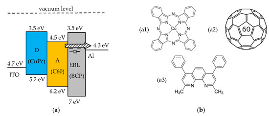
Figure 3.
(a) Open circuit band diagram of a three-layer D-A solar cell with exciton blocking layer (EBL). The arrow indicates electrons transport through defect states in the EBL; (b) Molecular structure of the organic materials used for the fabrication of the SCs (b1) CuPc, (b2) C60, and (b3) BCP.
2. Materials and Methods
This section describes the D-A three-layer SCs fabricated by the authors. The organic materials are Copper phtalocyanine (CuPc, Sigma-Aldrich product nr. 546674), used as the D organic material, fullerene (C60, ABCR product nr. AB109139) as the A organic material, and bathocuproine (BCP, Sigma-Aldrich product nr. 140910) as the material for the EBL. The molecular structures of these materials are shown in Figure 3b. The relevant HOMO and LUMO energy levels are shown in the band diagram of the three-layer D-A organic SC in Figure 3a.
Measured exciton diffusion lengths of many organic materials are reported in [10], including some spreading range for their values. The C60 has an exciton diffusion length LA = 40 nm whereas the CuPc has a much shorter exciton diffusion length LD = 5 nm [13]. Due to the very low charge carrier mobility in amorphous organic materials, it is convenient to choose the thicknesses of the D and A layers close to their respective exciton diffusion length [10]. As a matter of fact excitons can be efficiently dissociated only within an exciton diffusion length from the D-A interface. Moreover, due to the low mobility, most charge carriers can be collected at the electrodes only if the layers are not too thick. Based on those considerations, we chose 40 nm for the thickness of the A layer and 20 nm for the D layer. To prevent the damage-induced states from reaching the A layer, the thickness of the EBL (BCP) must be not too thin but also not too thick for allowing electrons to flow through it and achieving a low series resistance of the SC. Based on the study reported in [14], we chose a thickness of 12 nm.
All devices are fabricated in a single run by thermal evaporation in high vacuum (5 × 10⁻⁷ mbar) on commercial ITO-coated glass substrates (Merck Display Technologies, ITO film 100 nm thick with sheet resistance < 20 Ω/□). Suitable metal masks are used in close proximity of the substrate for delimiting the areas to coat with the organic layers and the metal cathode. The organic materials are used as received (i.e., no further purification) and deposited from Molibdenum boats at a rate of 2 Å/s, as measured by a quartz microbalance. The Al cathode is deposited from Tungsten coils, at a rate of 4 Å/s. ITO patterning is made by optical photolithography and wet etching. Figure 4a shows a top view of the devices, with a common 3 mm wide ITO strip for the anode. The organic materials are deposited first, through a rectangular mask. Next, the four Aluminum 3 mm wide strips are deposited, through another mask. The sample shown in Figure 4a includes four SCs, each with a 9 mm2 area.
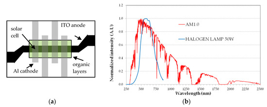
Figure 4.
(a) Top view of the layers arrangement for the sample with 4 organic solar cells of 9 mm2 area each. Black area is ITO film, grey stripes are Al film; (b) Spectrum of the halogen lamp as compared to the AM1.0 solar spectrum.
3. Photoelectrical Characterization
The SCs are tested in ambient atmosphere and without encapsulation immediately after film deposition. For a quick test of the devices, a commercial 50 W Tungsten halogen lamp is used as light source and the desired incident optical power density is set by simply varying the vertical distance between the lamp and the SC surface. The halogen lamp optical spectrum, measured by an Ocean Optics USB4000 UV-VIS fiber optic spectrometer limited to the 200–850 nm spectral range, is acceptably close to the visible part of the AM1.0 solar spectrum, as shown in Figure 4b. The decreasing lamp emission above 700 nm is not relevant here because the SC absorption is very small, due to the large HOMO-LUMO bandgaps. The optical spectrum is used to calibrate the light intensity of the halogen lamp and then to set the distance between the lamp and the SC surface for a standard value of 100 mW/cm2 for the incident optical power density. The current density J vs. forward voltage V is measured by a Keithley 6487 source-meter.
A typical J-V plot for the organic SC is reported in Figure 5a for a range of incident optical power density, from 45 mW/cm2 to 150 mW/cm2. We notice a good photovoltaic effect and a current density fairly monotonic with the increasing incident optical power density. This indicates minimum saturation effects at the used values of incident optical power density. The dark current results in a few μA/cm2. At 100 mW/cm2, the SC exhibits VOC = 0.45 V and JSC = 2.35 mA/cm2 with a fill factor FF ≈ 50%.
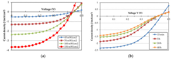
Figure 5.
(a) J-V characteristics of the best SC under illumination with increasing incident optical power density; (b) J-V characteristics of the best SC with time under continuous illumination at 100 mW/cm2 incident power density.
The external quantum efficiency (EQE) of a solar cell is the ratio electrons/s to incident photons/s. The electrons/s are calculated from JSC and the photons/s are calculated from the incident optical power and its optical spectrum. This gives EQE ≈ 5%. The power conversion efficiency (PCE) is the ratio of the maximum electric power the SC can deliver to an optimum load to the incident optical power. The PCE is calculated to be about 0.5%. Both EQE and PCE values are lower than previously reported for SC with similar structure [10] and this can be ascribed to the low value of JSC being about one order of magnitude smaller. In fact to get a high value of EQE and PCE one must have a high Jsc and VOC with FF close to 1.
A low JSC is mainly due to excitons loss at non radiative recombination sites for both Frenkel excitons in the D and A organic layers and CT excitons at the D/A interface. These non radiative recombination sites can have different origins. (i) foreign impurities incorporated in the organic layers because the organic materials used for thin film deposition are not purified, (ii) trapping defects created in the organic layers by the exposure of the SC to oxygen and water (humidity) [15,16] because our SCs are non encapsulated and operated in ambient atmosphere. Moreover some structural disorder and traps could also have been generated and propagated through the EBL in the A layer during metal cathode deposition and this will add a further non radiative recombination path for Frenkel excitons in the A layer. However we are not able to give proof for the latter hypothesis.
4. Lifetime Tests
Organic materials are very sensitive to oxygen and water (humidity) present in ambient atmosphere and this can lead to degradation of the performances and eventually to device breakdown [15,16]. For evaluating the aging rate, we measured the J-V characteristics of the SC with time under continuous illumination, with 100 mW/cm2 incident power density. The results are shown in Figure 5b. A slight decrease in VOC and a substantial decrease in JSC is evident in a time interval of 48 h. The J-V curves get less steep with time and this means that the SC attains a higher series resistance RS and a decreasing fill factor FF.
The values of VOC, JSC, RS and FF with time are shown in Figure 6. The series resistance of the SC is calculated from the slope of the J-V curve above VOC (forward bias). Moreover the fill factor is calculated as:
where Pmax is the maximum electric power the SC can deliver to an optimum load, VOC is the open circuit voltage, ISC is the short circuit current and VOC ISC is the absolute maximum power the SC could ideally deliver. Pmax is easily derived from the J-V curves. From Figure 6a after 5 h the short circuit current density decreases of about 25% as compared to the value at 15 min and then the decrease rate of the short circuit current density slows down with time reaching about 40% after 48 h. Figure 6b shows the RS and FF vs. time. It can be noticed that, after 5 h, RS almost quadruplicates and then continues to increase at a smaller rate. The FF decreases from 50% to about 40% after 5 h time and so by a relatively small amount and then again the decrease slows down.
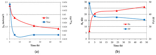
Figure 6.
(a) Short circuit current density JSC and open circuit voltage VOC; (b) Series resistance RS and fill factor FF as a function of time for the best SC under continuous illumination at 100 mW/cm2 incident power density.
In summary, an initial relatively fast degradation takes place within five hours from fabrication. Then the degradation progresses at a lower rate. A proper encapsulation in inert atmosphere [17,18] of the devices is found to be effective in preventing oxygen and water molecules (extrinsic factors) from diffusing into the organic layers. In fact chemical reactions with oxygen and water molecules are the dominant degradation mechanism in air. On the contrary, encapsulated organic SCs have durability and lifetime dominated by photoelectric and thermal stability (intrinsic factors) of the organic materials.
5. Conclusions
In this paper we report our experience in the fabrication of organic SCs having the D-A heterojunction structure with EBL. The best devices exhibit an open circuit voltage VOC = 0.45 V, a short circuit current density JSC = 2.35 mA/cm2 with a fill factor FF ≈ 50%, an external quantum efficiency (electrons/s over incident photons/s) EQE ≈ 5% and a power conversion efficiency of about 0.5%. Non-encapsulated devices are very sensitive to oxygen and humidity induced degradation. This degradation process was monitored in a time interval of 48 h. Our results confirm that non-encapsulated organic solar cells have limited stability in ambient atmosphere.
Author Contributions
Conceptualization, P.C.; methodology, P.C.; investigation, P.C.; resources, P.C. and C.A.; data curation, P.C.; writing—original draft preparation, P.C. and C.A.; writing—review and editing, C.A., M.A.G. and A.P.; funding acquisition, P.C. All authors have read and agreed to the published version of the manuscript.
Funding
This research was funded by University of Palermo, under grant number ORPA073ZR8 “Organic solar cells development”.
Acknowledgments
In this section you can acknowledge any support given which is not covered by the author contribution or funding sections. This may include administrative and technical support, or donations in kind (e.g., materials used for experiments).
Conflicts of Interest
The authors declare no conflict of interest.
References
- Pope, M.; Swenberg, C.E. Electronic Processes in Organic Crystals and Polymers, 2nd ed.; Oxford University Press: New York, NY, USA, 1999. [Google Scholar]
- Sun, S.-S.; Dalton, L.R. Introduction to Organic Electronic and Optoelectronic Materials and Devices; CRC Press: Boca Raton, FL, USA, 2008. [Google Scholar]
- Rand, B.P.; Richter, H. Organic Solar Cells: Fundamentals, Devices, and Upscaling; CRC Press: Boca Raton, FL, USA, 2014. [Google Scholar]
- Luo, G.; Ren, X.; Zhang, S.; Wu, H.; Choy, W.C.; He, Z.; Cao, Y. Recent advances in organic photovoltaics: Device structure and optical engineering optimization on the nanoscale. Small 2016, 12, 1547–1571. [Google Scholar] [CrossRef] [PubMed]
- Scharber, M.C.; Sariciftci, N.S. Efficiency of bulk-heterojunction organic solar cells. Prog. Polym. Sci. 2013, 38, 1929–1940. [Google Scholar] [CrossRef] [PubMed]
- Green, M.A.; Ho-Baillie, A.H.; Snaith, J. The emergence of perovskite solar cells. Nat. Photonics 2014, 8, 506–514. [Google Scholar] [CrossRef]
- Wan, Q.; Guo, X.; Wang, Z.; Li, W.; Guo, B.; Ma, W.; Zhang, M.; Li, Y. 10.8% Efficiency polymer solar cells based on PTB7 TH and PC 71 BM via binary solvent additives treatment. Adv. Funct. Mater. 2016, 26, 6635–6640. [Google Scholar] [CrossRef]
- Balderrama, V.S.; Estrada, M.; Han, P.L.; Granero, P.; Pallarés, J.; Ferré-Borrull, J.; Marsal, L.F. Degradation of electrical properties of PTB1:PCBM solar cells under different environments. Sol. Energy Mater. Sol. Cells 2014, 125, 155–163. [Google Scholar] [CrossRef]
- Tang, C.W. Two-layer organic photovoltaic cell. Appl. Phys. Lett. 1986, 48, 183–185. [Google Scholar] [CrossRef]
- Peumans, P.; Yakimov, A.; Forrest, S.R. Small molecular weight organic thin-film photodetectors and solar cells. J. Appl. Phys. 2003, 93, 3693–3723. [Google Scholar] [CrossRef]
- Peumans, P.; Bulović, V.; Forrest, S.R. Efficient photon harvesting at high optical intensities in ultrathin organic double-heterostructure photovoltaic diodes. Appl. Phys. Lett. 2000, 76, 2650–2652. [Google Scholar] [CrossRef]
- Rand, B.P.; Li, J.; Xue, J.; Holmes, R.J.; Thompson, M.E.; Forrest, S.R. Organic double-heterostructure photovoltaic cells employing thick tris(acetylacetonato)ruthenium(iii) exciton-blocking layers. Adv. Mater. 2005, 17, 2714–2718. [Google Scholar] [CrossRef]
- Mikhnenko, O.V.; Blom, P.W.M.; Nguyen, T.-Q. Exciton diffusion in organic semiconductors. Energy Env. Sci. 2015, 8, 1867–1888. [Google Scholar] [CrossRef]
- Hong, Z.R.; Huang, Z.H.; Zeng, X.T. Utilization of copper phthalocyanine and bathocuproine as an electron transport layer in photovoltaic cells with copper phthalocyanine/buckminsterfullerene heterojunctions: Thickness effects on photovoltaic performances. Thin Solid Films 2007, 515, 3019–3023. [Google Scholar] [CrossRef]
- Song, Q.L.; Wang, M.L.; Obbard, E.G.; Sun, X.Y.; Ding, X.M.; Hou, X.Y.; Li, C.M. Degradation of small-molecule organic solar cells. Appl. Phys. Lett. 2006, 89, 251118. [Google Scholar] [CrossRef]
- Hermenau, M.; Riede, M.; Leo, K.; Gevorgyan, S.A.; Krebs, F.C.; Norrman, K. Water and oxygen induced degradation of small molecule organic solar cells. Sol. Energy Mater. Sol. Cells 2011, 95, 1268–1277. [Google Scholar] [CrossRef]
- Luo, D.; Yang, Y.; Xiao, Y.; Zhao, Y.; Yang, Y.; Liu, B. Regulating charge and exciton distribution in high-performance hybrid white organic light-emitting diodes with n-type interlayer switch. Nano-Micro Lett. 2017, 9, 37. [Google Scholar] [CrossRef] [PubMed]
- Mai, R.; Wu, X.; Jiang, Y.; Meng, Y.; Liu, B.; Hu, X.; Roncalie, J.; Zhou, G.; Liu, J.; Kempa, K.; et al. An efficient multi-functional material based on polyethersubstituted indolocarbazole for perovskite solar cells and solution-processed non-doped OLEDs. J. Mater. Chem. A 2019, 7, 1539–1547. [Google Scholar] [CrossRef]


© 2020 by the authors. Licensee MDPI, Basel, Switzerland. This article is an open access article distributed under the terms and conditions of the Creative Commons Attribution (CC BY) license (http://creativecommons.org/licenses/by/4.0/).