Article

Reduced Tilting Effect of Smartphone CMOS Image Sensor in Visible Light Indoor Positioning

by
Md Habibur Rahman
,
Mohammad Abrar Shakil Sejan
,
Jong-Jin Kim
* and
Wan-Young Chung
*
Department of Electronic Engineering, Pukyong National University, Busan 48513, Korea
*
Authors to whom correspondence should be addressed.
Electronics 2020, 9(10), 1635; https://doi.org/10.3390/electronics9101635
Submission received: 27 August 2020 / Revised: 29 September 2020 / Accepted: 30 September 2020 / Published: 3 October 2020
(This article belongs to the Special Issue New Challenges in Wireless and Free Space Optical Communications)

Abstract

:
Visible light positioning (VLP) using complementary metal–oxide–semiconductor (CMOS) image sensors is a cost-effective solution to the increasing demand for an indoor positioning system. However, in most of the existing VLP systems with an image sensor, researchers assume that the receiving image sensor is positioned parallel to the indoor floor without any tilting and, thus, have only focused on the high-precision positioning algorithm and ignored the proper light-emitting diode (LED)-ID recognition. To address these limitations, we present, herein, a smartphone CMOS image sensor and visible light-based indoor localization system for a receiver device in a tilted position, and we have applied a machine learning approach for optimized LED-ID detection. For detection of the LED-ID, we generated different features for different LED-IDs and utilize a machine learning method to identify each ID as opposed to using the conventional coding and decoding method. An image processing method was used for the image features extraction and selection. We utilized the rolling shutter mechanism of the smartphone CMOS image sensor in our indoor positioning system. Additionally, to improve the LED-ID detection and positioning accuracy with the tilting of the receiver, we utilized the embedded fusion sensors of the smartphone (e.g., accelerometer, gyroscope, and magnetometer, which can be used to extract the yaw, pitch, and roll angles). The experimental results for the proposed positioning system show that it can provide 2.49, 4.63, 8.46, and 12.20 cm accuracy with angles of 0, 5, 10, and 15°, respectively, within a 2 m × 2 m × 2 m positioning area.

1. Introduction

Due to the increasing demand for a localization system for indoor environments, visible light indoor positioning has attracted considerable attention for location-based services in the new research community. The global positioning system (GPS) works quite adequately for providing positioning information in the outdoors environment. However, because of difficulties in propagating the GPS signal in indoor areas, the GPS cannot provide satisfactory performance in this environment. Therefore, there are many alternative techniques used for indoor positioning, and these include the use of the flight time for Wi-Fi signals [1], radiofrequency (RF) identification [2], ultrawideband [3], and ZigBee [4] in triangulation. Among these techniques, RF-based positioning offers low cost and good coverage [5]. However, because of multipath fading and signal interference, the accuracy of their RF-based positioning is still uncertain, the radiation is harmful to the human body, and its use is restricted to a certain location such as hospitals, aircraft, and mines. The accuracy of ultrasonic positioning systems [6] can be extremely high. However, additional infrastructure is required for system installations. By contrast, visible light communication (VLC) is a reliable technology; it offers high data transfer rates, is environmentally friendly, and ensures secure communication in an indoor environment [7].
Many positioning methods using visible light have been proposed, and they can determine positioning by applying time-of-arrival, angle-of-arrival, and vision analyses [8]. Several smartphone image sensor-based visible light positioning (VLP) have been proposed and implemented in recent years [9,10,11,12]. The use of visible light, image sensors, and a machine learning approach has been proposed for indoor light-emitting diode (LED)-ID detection in the indoor positioning has proposed in [13,14]. In [14], the authors used double-LED positioning algorithms with an industrial camera image sensor and did not consider the tilt angle during the experiment. The proximity-based positioning method with the utilized industrial camera cannot provide the exact positioning information during positioning estimation and the authors also did not consider the receiver device angle effect at the time of the experiment in [13]. In addition, use of an industrial camera as a visible light indoor positioning system is impractical because it is not suitable for handheld use or compatible with user mobility within the experimental region.
In recent studies [15,16,17], VLP by smartphone inertial sensor, magnetic sensor, accelerometer sensor, and other supported devices has been used to improve position accuracy. Three-dimensional VLC-based indoor positioning systems considering receiver tilt and using received signal strength have also been reported [18]. In [18], a photodiode (PD) is used as the receiver, but it is difficult to implement this in a VLP system capable of considering the tilt of the receiver. The system also requires extra hardware that makes it complicated and costly. A large scale VLP system with a receiver orientation system and tilting effect has been reported [19]. In that work, the authors used a PD receiver and employed the traditional decoding and encoding technique for modulation in the transmitter. A visible light-based positioning system considering receiver tilting angle during position estimation has been reported in [20]. The receiver device is not clear, and it provides simulation-based performance with a small-scale positioning area.
After consideration of the above studies, we have developed and present herein, a VLP system based on visible light and complementary metal–oxide–semiconductor (CMOS) image sensor. With this system, we considered the effect of receiver device tilting and have used a machine learning approach for the LED-ID detection techniques. We generate different features for the different LED-IDs and utilize machine learning methods to identify each ID, rather than reply on the conventional coding and decoding method. The image processing method was used for the extraction and selection of the image features. We also used the smartphone CMOS image sensor rolling shutter mechanism in our proposed positioning system. Additionally, to improve the LED-ID detection and positioning accuracy for various orientations of the receiver, we utilized the embedded smartphone fusion sensors (accelerometer, gyroscope, and magnetometer) to extract yaw, pitch, and roll angles. Experimental results show that the proposed positioning system can provide 2.49, 4.63, 8.46, and 12.20 cm accuracy with angles 0, 5, 10, and 15°, respectively, within a 2 m × 2 m × 2 m positioning area.
The rest of this paper is organized as follows: The system design is described in Section 2, the proposed positioning method is discussed in Section 3, and the experimental environment and the outcomes of this study are presented in Section 4. Finally, conclusions based on this work are presented in Section 5.

2. System Architecture

2.1. Transmitter Section

2.1.1. Transmitter Design

Figure 1 contains a schematic of the transmitter system, which consists primarily of three parts: (1) an LED bulb, (2) a metal–oxide–semiconductor field-effect transistor (MOSFET) chip, and (3) a microcontroller unit (MCU) chip. A circular white LED with a 15 cm diameter, and 15 W power capacity was used as a transmitter LED. To control the current of the LED bulb, we constructed a driver circuit comprising a high-speed switching MOSFET device with two parallel resistors R 1 and R 2 . The resistor R 1 was connected to the data pin of the MCU, and resistor R 2 was connected with pin number three of the MOSFET. An ATmega328p [21] MCU was used to encode the data for the LED lighting. Table 1 shows the parameters of the components used for transmitting data.

2.1.2. Transmitter LED Modulation

To avoid the flickering problem typical of general on–off keying modulation techniques, we used pulse width modulation (PWM) with variable frequency in this system, and the different duty ratios are shown in Figure 2. The transmitter LED flickering is controlled according to the modulation frequency used during the transmission process. However, for frequencies below 200 Hz, human eyes can observe the flicker [23]. As human eyes can recognize visual flicker at a modulation frequency less than 200 Hz, the frequency for modulation is generally between 200 Hz to 8 kHz. In the proposed system, we control the flickering by adopting different frequencies for different LED-IDs using frequencies greater than 200 Hz. In the receiver section, we used the smartphone CMOS image sensor; after configuring the smartphone camera parameters, we could capture each LED lighting image with the CMOS image sensor. The images for different LEDs modulated by the different duty ratios and frequencies are shown in Figure 3. The duty ratios of the bright strips are different, and the number of bright strips on the image plane is the same for a given the distance between transmitter LEDs and a receiver smartphone camera. Therefore, the number of bright strips depends on the distance between transmitter and receiver. Figure 3 shows the image captured from different LED-IDs with different duty ratios and strips widths.

2.2. Receiver Section

2.2.1. Rolling Shutter Operation of Smartphone Embedded CMOS Image Sensor

The operation of the rolling shutter of the smartphone CMOS image sensor is shown in Figure 4. The working mode for the CMOS image sensor requires that the exposure and data readout time be executed by scanning the pixels of every dark and bright strip row by row. By switching between ON and OFF states of the LED during data transmission, dark and bright strips appeared for the image captured by the CMOS image sensor. The rolling shutter mechanism allows each row of pixels to be individually scanned and provides a high frame rate speed.

2.2.2. Smartphone Camera Configuration

In our VLP system, we developed a camera application for the receiver on the Android Studio platform. We manually configured some camera parameters to capture the image data without distortion. For the configuration of the camera, we focused primarily on two parameters, namely, exposure time and ISO. Table 2 shows the parameters of the components used for the receiver section.
Exposure is the time during which the camera shutter is open to allow light into the photodiode matrix, and it is defined as the time required for the collection of a pixel. The pixels are the light-induced charge accumulated until saturation is reached.
In a smartphone camera, ISO indicates the number of photons required to saturate the pixel. The higher ISO value, fewer photons required to reach saturation. Therefore, as the ISO value increases, the probability of pixel saturation will increase; in this case, the widths of the dark and bright stripes on the image plane will also increase.

2.2.3. Mechanism of LED-ID Feature Extraction and Selection

The LED-ID feature extraction process has been described in [13], where authors extracted three features in the image processing method. According to the feature generation process, to obtain a better recognition and detection rate during decoding and classification of each transmitting LED-ID, we complemented with three features (bright strip no., duty ratio, area of the LED) when we were training the system in the offline process. Frequency is a predefined feature of each modulated LED, and it was valuable feature during the training process. The overall process for the extraction of LED features is shown in the block diagram in Figure 5. According to the figure, by using an image processing method, it requires four steps to be completed for feature extraction.
First, the original image captured by the smartphone CMOS image sensor must be converted into a grayscale image. Further, the grayscale image is converted into a binary image, and then the color labels of the RGB image are applied. Finally, the image segmentation method is applied. The image segmentation process for the image captured by smartphone CMOS image sensor is shown in Figure 6a–f. The mechanism for determining the extraction numbers of the bright strips by the image processing method is shown in Figure 7a–e, where Figure 7a represents the grayscale image from the original capture image, Figure 7b indicates the histogram for the threshold value of the original image with the gray level for counting the pixels, the binary image converted from the grayscale image is represented by Figure 7c, and the RGB color image to detect and count each bright strip of the blob on the binary image is represented by Figure 7d. Finally, Figure 7e represents the binary image with bright strip count number.

2.3. LED-ID Identification Process

The LED-ID recognition for the transmission side was accomplished with the machine learning method, which is highly accurate and applicable for the classification of transmitter information in the VLP system. A typical linear classifier, linear support vector machine (SVM), is used to achieve the recognition of LED-IDs in the machine learning field. For the selection of training and testing samples, 5000 image data were taken at each position, where 4000 were used as the training samples and the other 1000 were used as testing samples. The average training time was 2.56 s and the total image processing/classifying time was 17.36 ms. The identification process is described in detail below.

Support Vector Machine

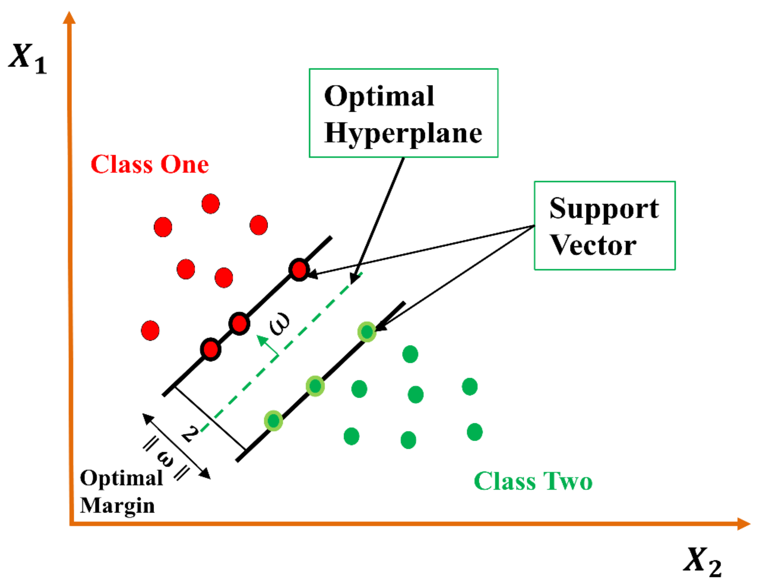
We applied different duty ratios and modulated frequencies to four different LED transmitters for the extraction of the different LED-ID features from all of the transmitters by the process described in Section 2.2.3 above. Table 3 shows the part of the sample input data which are extracted from the ID extraction process. To obtain accurate positioning information, we must decode or recognize the LED-ID information properly; otherwise, the system requires repositioning, and this increases the system latency. For this reason, we separate all of the LED features by applying SVM to classify each LED-ID by their feature characteristics. SVM works based on the concept of the decision planes that define the decision boundaries. The decision plane is to separate between a set of objects having different classes. For the LED feature extraction process with linearly separate different data samples, the optimal classification hyperplane can separate the instances into two classes, as shown in Figure 8 [24]. Let us define the class case as Xj, where j = 1, 2, 3..., N. Here, in our case, N = 4 be the feature vector of training data set X. These belong to either of the two classes, ω1 and ω2, which are linearly separable. The general SVM classification can be described as a mathematical optimization problem: a r g m i n   1 2   ω 2 s.t. y j ω T X j + b 1 . The goal is to find the hyperplane that classifies all the training vectors correctly which can be expressed as f(X) = ωT·X + b where the direction of the hyperplane is represented by ω, which has the same dimensions as X , the transpose of ω is defined as ωT, and the appropriate position of the hyperplane in space is indicated by b. The hyperplane is not the identical such that we can write the geometrical margin as o = f X ω , which represents the geometrical distance between the data samples to the hyperplane. To obtain the optimal value of the hyperplane, we aim to maximize o . As the value of |f(X)| can be changed by scaling ω and b when making it equal to 1 and the solution we have obtained from the maximum value of 1 ω . We can solve the problem by utilizing the Lagrange multiplier, and the problem comes to be solved by f X = j = 1 n y j α j X , X j + b where yj is the class indicator of X j (+1 for ω1 and −1 for ω2), the Lagrange multiplier is indicated by αj and, finally, the inner vector inner product is defined by X , X j .

3. Positioning Method

3.1. Overview of Proposed System

The proposed positioning method is deployed using VLC and by the most popular smartphone image sensor. It consists of two stages: the offline stage and the online stage. Figure 9 shows an overview of the proposed positioning system process.
In the process of the offline stage, the number of LED project strips in the image sample was captured by the smartphone CMOS image sensor via the rolling shutter mechanism. The image processing method was then applied for extracting and counting each LED image feature. Subsequently, the machine learning method was applied to build the classifier in accordance with the obtained data features. Finally, the LED-ID library was completed to finalize the structure.
During the online stage, the image data from the library were separated according to the number of strips and modulated LED with ID pairs. The camera image sensor then recognized the LED project ID within the camera field of view. Subsequently, the establishment of the image sensor position was used to calculate the distance between the LED coordinate and image sensor coordinate. Smartphone embedded sensors (accelerometer, gyroscope, and magnetometer) were used to extract yaw, pitch, and roll angles and improve the recognition accuracy during acquisition of the positioning information by the proposed system.

3.2. Positioning Algorithm

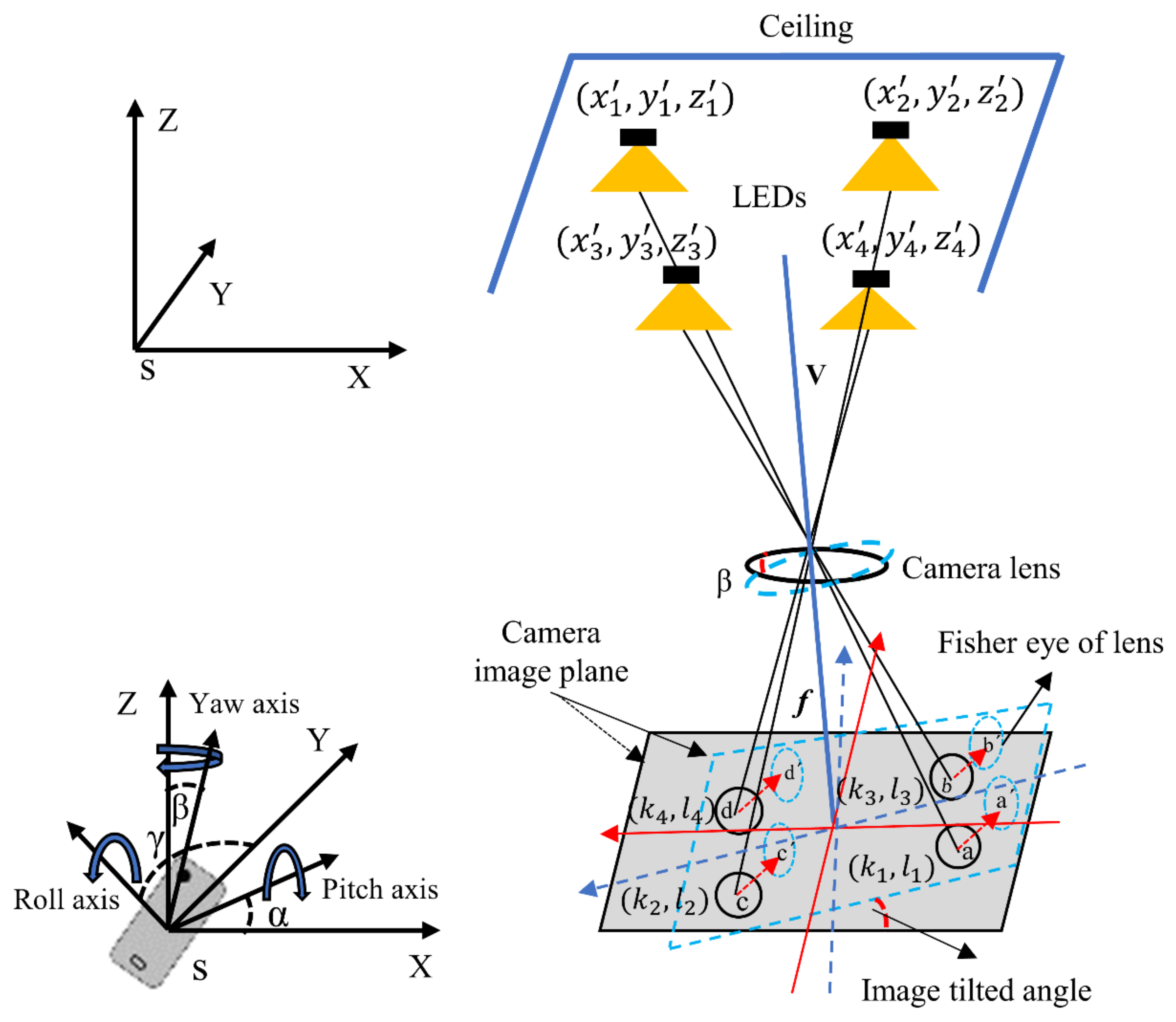
The positioning system architecture consists of a transmitter and receiver, as shown in Figure 10. The coordinates of the LED in the world coordinate system are x 1 , y 1 , z 1 , x 2 , y 2 , z 2 , x 3 , y 3 , z 3 , and x 4 , y 4 , z 4 , which are known. V is the vertical distance from the lens center of the CMOS image sensor to the fixed point of the LED. The camera focal length is f, which is an intrinsic parameter of every camera CMOS image sensor. The LED coordinates of the image coordinate system are defined as (k1, l1), (k2, l2), (k3, l3), and (k4, l4), respectively, which can be obtained from the LED coordinate on the pixel plane. The origin point of image coordinate system is the intersection point between the camera optical axis of the camera and imaging plane of the CMOS image sensor. The unit of the coordinate system is mentioned as mm (millimeter) and the unit of the pixel coordinate is pixel, which is described by rows and lines of the pixels. Therefore, when obtaining the pixel coordinates of an LED by camera, the coordinates of an LED in the image coordinate system can be calculated by the relationship between the pixel coordinate and image coordinate which is expressed as follows.
kn = (i − i0)dkn
ln = (j − j0)dln
where kn and ln donate the image coordinate system, and i and j denote the pixel coordinate system, which we can extract via the image processing mechanism of receiving an image on the image plane. Variables dkn and dln represent the unit image transformation coordinate systems. The centers of the coordinate system of the image are represented as i0 and j0, respectively. To ensure that we can get the image coordinate system after that, we can calculate the distance L of the LED in the image coordinate system and the distance M of the LED in the world coordinate system. Therefore, the distance L can be expressed as
L = k 1 k 2 2 + l 1 l 2 2 .
However, the distance M can be expressed as
M = x 1 x 2 2 + y 1 y 2 2 .
According to the camera operating principle, the vertical distance V between the camera lens and the LED can be obtained, and the z’ coordinate can be calculated from the distance, which is expressed as
V = M L f
where f is the camera focal length and is a known parameter of every smartphone image sensor. Therefore, the z m coordinate of the image sensor from the four LEDs can be written as
z m = z 1 V =   z 2 V = z 3 V = z 4 V .
At the origin on the image plane, the image coordinate system is generated, and if we consider that the Dn is the origin point and n = 1, 2, 3, 4..., we can express the relation as
D n = k n 2 + l n 2 .
Therefore, according to the camera operating principle, the horizontal distance Hn between the image sensor in the world coordinate system and the LED can be expressed as
H n = M L D n .
However, the distances Hn, where n = 4, from multiple LEDs and the smartphone image sensor can be expressed as
H 1 = x m x 1 2 + y m y 1 2 + z m z 1 2 H 2 = x m x 2 2 + y m y 2 2 + z m z 2 2 H 3 = x m x 3 2 + y m y 3 2 + z m z 3 2 H 4 = x m x 4 2 + y m y 4 2 + z m z 4 2 .
After evaluation of Equation (9), we can write the following expression:
{ H 1 H 2 = 2 x 2 x 1 x m + 2 y 2 y 1 y m + 2 z 2 z 1 z m + x 1 2 + y 1 2 + z 1 2 x 2 2 y 2 2 z 2 2 H 1 H 3 = 2 x 3 x 1 x m + 2 y 3 y 1 y m + 2 z 3 z 1 z m + x 1 2 + y 1 2 + z 1 2 x 3 2 y 3 2 z 3 2 H 1 H 4 = 2 x 4 x 1 x m + 2 y 4 y 1 y m + 2 z 4 z 1 z m + x 1 2 + y 1 2 + z 1 2 x 4 2 y 4 2 z 4 2
Therefore, the smartphone image coordinates (xm, ym, zm) will be
[ x m y m z m ] = 1 2 x 2 x 1 y 2 y 1 z 2 z 1 x 3 x 1 y 3 y 1 z 3 z 1 x 4 x 1 y 4 y 1 z 4 z 1 1 H 1 H 2 x 1 2 + y 1 2 + z 1 2 x 2 2 y 2 2 z 2 2 H 1 H 3 x 1 2 + y 1 2 + z 1 2 x 3 2 y 3 2 z 3 2 H 1 H 4 x 1 2 + y 1 2 + z 1 2 x 4 2 y 4 2 z 4 2 .

3.3. Smartphone Rotation Model

In recent years, modern smartphones have been equipped with many sensors. To determine the orientation of the smartphone, an accelerometer, gyroscope, and magnetometer sensor are used, which respectively can give roll, pitch, and yaw angles during operation, as shown in Figure 11. Those angles can be denoted, as shown in Figure 10, as α, β, and γ, respectively. To provide the promising positioning system with accurate information regarding the user terminal device, those embedded sensors are used during user movement and with different device orientations in the positioning environment. However, accurately estimating these angles from the built-in sensor is practically challenging because of the hardware quality and different noise issues such as thermal noise of the magnetometer and mechanical noise of the accelerometer sensors. In prior work [25,26,27], the authors reported a different method for improvement and performance analysis of the positioning information by measuring sensor data. In this study, our goals are to establish a positioning system by using the smartphone embedded image sensor and use other embedded sensors to observe the performance of the system with various orientations effect of the smartphone. However, the measurements of the sensor angles (α, β, and Υ) with VLC and the image sensor could be used to enhance the positioning accuracy with the proposed positioning method and also to simplify the system. The rotation theorem from Euler’s proposal explains that in three-dimensional space, any displacement of a rigid body at a fixed point is equal to a single rotation about some axis that runs through that fixed point [28]. According to the relationship between the rotation angle R =   R α R β R γ of the device and the normal vector m of the device, we can express that relation as
m = R m = R α R β R γ m
where m and m are the device normal vectors before and after rotation, respectively [29]. Moreover, R α R β R γ is the rotation angle resulting from the roll, pitch, and yaw along the x′, y′, and z′ axes, respectively. Let us consider that the world and the initial device coordinates of the normal vector m = 0 , 0 , 1 T ; after applying the rotation matrices, the corresponding normal rotation vector [29] from Equation (12) can be expressed as
m = R α R β R γ 0 0 1 = cos α sin α 0 sin α cos α 0 0 0 1 1 0 0 0 cos β sin β 0 sin β cos β cos γ 0 sin γ 0 1 0 sin γ 0 cos γ 0 0 1
m = cos γ sin α sin β + cos α sin γ sin α sin γ cos α cos γ sin β cos β cos γ .
The normal vector for the rotated device, m , is represented in the world coordinate system with the corresponding polar angle (θ) and azimuth (ω), respectively. The polar (θ) angle is the angle between the device normal vector m and along the positive z′ axis, and azimuth (ω) angle is the angle between the projection of a device normal vector, m from the xy′ plane and along the positive x′ axis. Polar and azimuth angle of the smartphone orientation are shown in Figure 12. However, the polar angle can be represented as cos θ =   m . z ^   m where z ^ is the unit vector along the z′ axis. Therefore, the polar angle can be obtained from Equation (14) as
θ = cos 1 cos β cos γ .
From Equation (15), it is understood that the polar angle of the device is primarily dependent on the roll and pitch angle that is associated with the human movement during position estimation. However, the azimuth angle of the device can be represented by the fundamental rotation of the device which can expressed as
ω = tan 1 m y m x = tan 1 sin α sin γ cos α cos γ sin β cos γ sin α sin β + cos α sin γ .

4. Experiment and Results

4.1. Experimental Setup

The proposed positioning system was tested in an experimental work area with a floor space area measuring 2 m × 2 m, and the with the LED luminaire and camera image sensor mounted at a height of 2 m above the ground. The experimental setup for the proposed system comprised 4 LEDs mounted on the ceiling. The LEDs were spacing 2 m from each other and within the experimental area. Each of the LED luminaires transmitted their individual coordinate information to the smartphone camera image sensor, and the image sensor continuously received this coordinate information from the ceiling LED luminaires. Figure 13 shows the experimental environment. The CMOS image sensor captured image data and processed it with MATLAB software. Since, in this study, our focus is on the receiver image sensor orientation effect and testing the performance with tilt angles during location estimation, we considered those angles for our test with a smartphone (Samsung S8). Accordingly, we tested positioning accuracy when the smartphone was tilted at different heights by measuring roll, pitch, and yaw angles.

4.2. Experimental Results

4.2.1. LED-ID Recognition with Different Angle

The recognition of LED-ID depends on the distance between the LED transmitter and the smartphone image sensor receiver. The light intensity received by the CMOS image sensor drops because of the path loss for a line of sight communication and if the distance between the LED and image sensor increases. Additionally, the rate of recognition depends on the area of LED projection and the number of the dark and bright strips captured for the projected image. However, the width of dark and bright strips did not vary, but as the intensity of light at the receiving image has decreased, this affects the detection rate of the dark and bright strips during recognition of ID, and the recognition accuracy for each LED-ID also decreases.
To analyze the LED-ID recognition rate as a function of distance and sensor orientation angle, we modulated the LED transmitting data with PWM at 40%, 50%, 70%, and 80% duty ratio and 2, 3, 4, and 5 kHz variable frequency at a distance of up to 2 m, as shown in Figure 14. From Figure 14, we can see that the recognition rate for different tilt angles decreased with increasing communication distance between the transmitter and smartphone image sensor receiver. However, this performance is suitable for the accurate detection of LED-ID in any indoor setting.

4.2.2. Improved LED-ID Recognition Rate with Different Angle

Since we are using a smartphone image sensor with other embedded sensors to improve the recognition rates relative to those described previously in Section 4.2.1, we have benefited from the embedded sensor of the smartphone while measuring the orientation angle. After integrating the orientation sensor with our system, the recognition rate improved, and the LED-ID detection rate accuracy has improved, as shown in Figure 15. We can see from the figure that the recognition rate accuracy for all the tilt angles improved slightly. Additionally, the maximum allowable distance for ID detection increased slightly with sensor data addition during LED-ID recognition.

4.2.3. Performance Analysis of Positioning Accuracy

In our proposed system, the performance of the positioning accuracy analysis was determined for different angles of the smartphone during the experiment. To observe the performance of the proposed system as a function of angle, we measured the positioning accuracy at 0, 5, 10, and 15° as shown in Figure 16. From the figure, we can see that the location error increased with increasing smartphone tilt angle. Figure 16a shows the result with 0° tilt angle during the experiment for taking in a single estimation point, and the positioning error is approximately 2.49 cm. Figure 16b shows a positioning error of 4.63 cm with 5° tilt angle and Figure 16c,d show positioning errors of 8.46 and 12.20 cm for 10 and 15° tilts, respectively.
We also observed errors resulting from variations in the yaw, pitch, and roll angles, as shown in Figure 17. When the smartphone is tilted with respect to the x and y axes, the errors in position estimation are nearly identical for different tilt angles. However, various orientation with respect to the z axis consistently exhibited errors smaller than 3 cm.
For better visualization of system performance, Figure 18 shows that the cumulative distribution function (CDF) of the positioning errors for the different polar angles at 0, 5, 10, and 15°, respectively. The CDF is defined in terms of the probability of realizing a random positioning error (ε) whose value is less than or equal to the positioning accuracy Pa, such that the CDF can be expressed as (Pa) = P (ε ≤ Pa). As shown in Figure 18, the positioning error increases significantly as the polar angle increase from 0, 5, 10, and 15°, respectively, particularly for higher values of CDF percentage. During the experiment when the camera image sensor was tilted at greater than 15° angle, the lens of the camera became fish-eyed. The reason behind this is the radial distortion of the camera image sensor. Hence, we missed some bright strips during the image capture from the LED which eventually led to poor decoding accuracy of each LED-ID and increases in the positioning error. With polar angles ranging from 0 to 15°, the maximum error was seen to range from 7 to 18 cm, and after that, was unchanged. Therefore, it is perceivable that the proposed positioning method can achieve highly accurate positioning performance.

5. Conclusions

In most of the existing VLP systems that use an image sensor, researchers have assumed that the receiving image sensor is positioned completely parallel to the indoor floor without any tilting, and they have focused exclusively on the high-precision positioning algorithm. In this study, we implemented a positioning system based on VLC and smartphone CMOS image sensor so as to consider the effect of tilting during the estimation of position with the image sensor. We also utilized a machine learning approach for transmitter LED-ID recognition instead of the traditional coding and decoding method to improve the ID detection rate location accuracy. We considered the tilting of the image sensor over a 0 to 15° range and tested the effect of tilting on the position accuracy. We achieved centimeter-level position accuracies for different tilt angles of the smartphone terminal device; the degree of ID recognition was also very high when the compensating embedded sensors, such as accelerometer, gyroscope, and magnetometer, used the machine learning method to identify the IDs of the LED lights. In a future study, we intend to extend the size of the positioning area and improve system accuracy.

Author Contributions

For Conceptualization, W.-Y.C. and J.-J.K.; system methodology, M.H.R. and M.A.S.S.; software, M.H.R.; validation, W.-Y.C., J.-J.K. and M.H.R.; formal analysis, M.H.R. and M.A.S.S.; investigation, W.-Y.C., M.H.R. and M.A.S.S.; data curation, M.H.R.; writing—original draft preparation, M.H.R.; writing—review and editing, W.-Y.C., J.-J.K., M.H.R. and M.A.S.S.; supervision, W.-Y.C. and J.-J.K. All authors have read and agreed to the published version of the manuscript.

Funding

This work was supported by a Research grant of Pukyong National University (Year 2019).

Conflicts of Interest

The authors declare no conflict of interest.

References

  1. He, S.; Chan, S.H.G. Wi-Fi fingerprint-based indoor positioning: Recent advances and comparisons. IEEE Commun. Surv. Tutor. 2015, 18, 466–490. [Google Scholar] [CrossRef]
  2. Errington, A.F.; Daku, B.L.; Prugger, A.F. Initial position estimation using RFID tags: A least-squares approach. IEEE Trans. Instrum. Meas. 2010, 59, 2863–2869. [Google Scholar] [CrossRef]
  3. Cazzorla, A.; De Angelis, G.; Moschitta, A.; Dionigi, M.; Alimenti, F.; Carbone, P. A 5.6-GHz UWB position measurement system. IEEE Trans. Instrum. Meas. 2012, 62, 675–683. [Google Scholar] [CrossRef]
  4. Konings, D.; Budel, A.; Alam, F.; Noble, F. Entity tracking within a Zigbee based smart home. In Proceedings of the 2016 23rd International Conference on Mechatronics and Machine Vision in Practice (M2VIP), Nanjing, China, 28–30 November 2016; pp. 1–6. [Google Scholar]
  5. Çiftler, B.S.; Kadri, A.; Güvenç, I. Fundamental bounds on RSS-based wireless localization in passive UHF RFID systems. In Proceedings of the 2015 IEEE Wireless Communications and Networking Conference (WCNC), New Orleans, LA, USA, 9–12 March 2015; pp. 1356–1361. [Google Scholar]
  6. Kim, S.J.; Kim, B.K. Accurate hybrid global self-localization algorithm for indoor mobile robots with two-dimensional isotropic ultrasonic receivers. IEEE Trans. Instrum. Meas. 2011, 60, 3391–3404. [Google Scholar] [CrossRef]
  7. Pham, N.Q.; Rachim, V.P.; Chung, W.Y. High-accuracy VLC-based indoor positioning system using multi-level modulation. Opt. Express 2019, 27, 7568–7584. [Google Scholar] [CrossRef] [PubMed]
  8. Gu, Y.; Lo, A.; Niemegeers, I. A survey of indoor positioning systems for wireless personal networks. IEEE Commun. Surv. Tutor. 2009, 11, 13–32. [Google Scholar] [CrossRef] [Green Version]
  9. Rajagopal, N.; Lazik, P.; Rowe, A. Visual light landmarks for mobile devices. In Proceedings of the IEEE 13th International Symposium on Information Processing in Sensor Networks, Berlin, Germany, 15–17 April 2014; pp. 249–260. [Google Scholar]
  10. Kuo, Y.S.; Pannuto, P.; Hsiao, K.J.; Dutta, P. Luxapose: Indoor positioning with mobile phones and visible light. In Proceedings of the 20th Annual International Conference on Mobile Computing and Networking, Maui, HI, USA, 7–11 September 2014; pp. 447–458. [Google Scholar]
  11. Yang, Z.; Wang, Z.; Zhang, J.; Huang, C.; Zhang, Q. Wearables can afford: Light-weight indoor positioning with visible light. In Proceedings of the 13th Annual International Conference on Mobile Systems, Applications, and Services, Florence, Italy, 18–22 May 2015; pp. 317–330. [Google Scholar]
  12. Huang, H.; Feng, L.; Ni, G.; Yang, A. Indoor imaging visible light positioning with sampled sparse light source and mobile device. Chin. Opt. Lett. 2016, 14, 090602. [Google Scholar] [CrossRef]
  13. Xie, C.; Guan, W.; Wu, Y.; Fang, L.; Cai, Y. The LED-ID detection and recognition method based on visible light positioning using proximity method. IEEE Photonics J. 2018, 10, 1–16. [Google Scholar] [CrossRef]
  14. Guan, W.; Zhang, X.; Wu, Y.; Xie, Z.; Li, J.; Zheng, J. High precision indoor visible light positioning algorithm based on double LEDs using CMOS image sensor. Appl. Sci. 2019, 9, 1238. [Google Scholar] [CrossRef] [Green Version]
  15. Xie, B.; Chen, K.; Tan, G.; Lu, M.; Liu, Y.; Wu, J.; He, T. LIPS: A light intensity–based positioning system for indoor environments. ACM Trans. Sensor Netw. (TOSN) 2016, 12, 1–27. [Google Scholar] [CrossRef]
  16. Li, Z.; Yang, A.; Lv, H.; Feng, L.; Song, W. Fusion of visible light indoor positioning and inertial navigation based on particle filter. IEEE Photonics J. 2017, 9, 1–13. [Google Scholar] [CrossRef]
  17. Yasir, M.; Ho, S.W.; Vellambi, B.N. Indoor positioning system using visible light and accelerometer. J. Lightwave Technol. 2014, 32, 3306–3316. [Google Scholar] [CrossRef]
  18. Kim, D.; Park, J.K.; Kim, J.T. Three-dimensional VLC positioning system model and method considering receiver tilt. IEEE Access 2019, 7, 132205–132216. [Google Scholar] [CrossRef]
  19. Mai, D.H.; Le, H.D.; Pham, T.V.; Pham, A.T. Design and Performance Evaluation of Large-Scale VLC-Based Indoor Positioning Systems Under Impact of Receiver Orientation. IEEE Access 2020, 8, 61891–61904. [Google Scholar] [CrossRef]
  20. Jeong, E.-M.; Yang, S.-H.; Kim, H.-S.; Han, S.-K. Tilted receiver angle error compensated indoor positioning system based on visible light communication. Electron. Lett. 2013, 49, 890–892. [Google Scholar] [CrossRef]
  21. Microchip. Available online: https://www.microchip.com/wwwproducts/en/atmega328p (accessed on 1 October 2020).
  22. Vishay. Available online: https://www.alldatasheet.com/datasheet-pdf/pdf/436852/VISHAY/SIHP24N65E.html (accessed on 1 October 2020).
  23. Berman, S.M.; Greenhouse, D.S.; Bailey, I.L.; Clear, R.D.; Raasch, T.W. Human electroretinogram responses to video displays, fluorescent lighting, and other high frequency sources. Optom. Vis. Sci. 1991, 68, 645–662. [Google Scholar] [CrossRef] [PubMed]
  24. Theodoridis, S.; Koutroumbas, K. Pattern Recognition, 4th ed.; Academic: St. Louis, MO, USA, 2010; pp. 22–34. [Google Scholar]
  25. Patonis, P.; Patias, P.; Tziavos, I.N.; Rossikopoulos, D.; Margaritis, K.G. A fusion method for combining low-cost IMU/magnetometer outputs for use in applications on mobile devices. Sensors 2018, 18, 2616. [Google Scholar] [CrossRef] [PubMed] [Green Version]
  26. Kok, M.; Hol, J.D.; Schön, T.B. Using inertial sensors for position and orientation estimation. arXiv 2017, arXiv:1704.06053. [Google Scholar]
  27. Ayub, S.; Bahraminasab, A.; Honary, B. A sensor fusion method for smart phone orientation estimation. PGNET 2012. In Proceedings of the 13th Annual Postgraduate Symposium on the Convergence of Telecommunications, Networking & Broadcasting, Liverpool, UK, 25–26 June 2012. [Google Scholar]
  28. Kuipers, J.B.Q. A Primer with Applications to Orbits, Aerospace, and Virtual Reality; Princeton Univ. Press: Princeton, NJ, USA, 1999. [Google Scholar]
  29. Soltani, M.D.; Purwita, A.A.; Zeng, Z.; Haas, H.; Safari, M. Modeling the random orientation of mobile devices: Measurement, analysis and LiFi use case. IEEE Trans. Commun. 2018, 67, 2157–2172. [Google Scholar] [CrossRef] [Green Version]
Figure 1. Transmitter circuit connections and components.
Electronics 09 01635 g001
Figure 2. Transmitting PWM modulation data with different duty ratios.
Electronics 09 01635 g002
Figure 3. LED-ID modulation with different duty ratios: (a) 40% duty ratio; (b) 50% duty ratio; (c) 70% duty ratio; (d) 80% duty ratio.
Electronics 09 01635 g003
Figure 4. Rolling shutter operation of smartphone CMOS image sensor.
Electronics 09 01635 g004
Figure 5. Block diagram of LED-ID feature extraction mechanism.
Electronics 09 01635 g005
Figure 6. Mechanism of image segmentation: (a) captured original image; (b) grayscale image; (c) binary converted image; (d) closing operation of binary image; (e) region of interest detection of binary image; (f) segmentation of each image.
Electronics 09 01635 g006
Figure 7. Bright strips number calculation process: (a) grayscale image; (b) histogram of captured image; (c) converted binary image; (d) RGB color image with strip number; (e) bright strip number image.
Electronics 09 01635 g007
Figure 8. Linearly separable two class problem with linear classifier.
Electronics 09 01635 g008
Figure 9. Overview of the proposed positioning system with the mechanism of LED-ID reorganization.
Electronics 09 01635 g009
Figure 10. Architecture of the proposed positioning system with the transmitter and receiver sections.
Electronics 09 01635 g010
Figure 11. Mobile orientation scenario: (a) initial rotation position; (b) orientation along the z axis of yaw angle (α); (c) orientation along the x axis of pitch angle; (β); (d) orientation along the y axis of roll angle (γ).
Electronics 09 01635 g011
Figure 12. Polar and azimuth angle of the receiver orientation.
Electronics 09 01635 g012
Figure 13. Experiential test field with mapping area.
Electronics 09 01635 g013
Figure 14. LED-ID recognition rate versus communication distance with different SVM tilt angles.
Electronics 09 01635 g014
Figure 15. LED-ID improved recognition rate versus communication distance with different SVM at tilt angles.
Electronics 09 01635 g015
Figure 16. Positioning error performance at different angles: (a) error at 0° polar angle; (b) error at 5° polar angle; (c) error at 10° polar angle; (d) error at 15° polar angle.
Electronics 09 01635 g016
Figure 17. Positioning error at different angles: (a) error at pitch angle; (b) error at roll angle; (c) error at yaw angle.
Electronics 09 01635 g017
Figure 18. Cumulative distribution function (CDF) vs. positioning error at different polar angles.
Electronics 09 01635 g018
Table 1. Transmitter component parameters.
Parameters NameValues
LED ModelBSDW-010, Color Temp. 5300~6000 K
LED Size15 cm
LED Power15 W
Number of LEDs4
MCUAtmega328p
MOSFET ChipP24N65E [22]
Resistance R 1 10 kΩ
Resistance R 2 55 Ω
Modulation SchemePWM
Table 2. Receiver components parameters.
Parameters NameValues
Image SensorRolling Shutter CMOS Sensor
Shutter Speed32 kHz
ISO500
Frame Rate30 fps
Smartphone ModelSamsung Galaxy S8
CameraFront Camera with 8 megapixels
Focal Length24 mm
Aperture1.7
Camera APICamera 2 with API Level 25
Camera Image Resolution1080 × 920 pixels
Table 3. Sample of input LED features data.
LED-IDBright Strip no.Duty Ratio (%)Frequency (kHz)Area of LED (pixel)
ID-130.40025794
ID-230.50036712
ID-340.70048584
ID-440.800510,737