Article

Calculation of Semiconductor Power Losses of a Three-Phase Quasi-Z-Source Inverter

Faculty of Electrical Engineering, Mechanical Engineering and Naval Architecture, University of Split, 21000 Split, Croatia
*
Author to whom correspondence should be addressed.
Electronics 2020, 9(10), 1642; https://doi.org/10.3390/electronics9101642
Submission received: 14 September 2020 / Revised: 28 September 2020 / Accepted: 30 September 2020 / Published: 6 October 2020
(This article belongs to the Section Power Electronics)

Abstract

:
This paper presents two novel algorithms for the calculation of semiconductor losses of a three-phase quasi-Z-source inverter (qZSI). The conduction and switching losses are calculated based on the output current-voltage characteristics and switching characteristics, respectively, which are provided by the semiconductor device manufacturer. The considered inverter has been operated in a stand-alone operation mode, whereby the sinusoidal pulse width modulation (SPWM) with injected 3rd harmonic has been implemented. The proposed algorithms calculate the losses of the insulated gate bipolar transistors (IGBTs) and the free-wheeling diodes in the inverter bridge, as well as the losses of the impedance network diode. The first considered algorithm requires the mean value of the inverter input voltage, the mean value of the impedance network inductor current, the peak value of the phase current, the modulation index, the duty cycle, and the phase angle between the fundamental output phase current and voltage. Its implementation is feasible only for the Z-source-related topologies with the SPWM. The second considered algorithm requires the instantaneous values of the inverter input voltage, the impedance network diode current, the impedance network inductor current, the phase current, and the duty cycle. However, it does not impose any limitations regarding the inverter topology or switching modulation strategy. The semiconductor losses calculated by the proposed algorithms were compared with the experimentally determined losses. Based on the comparison, the correction factor for the IGBT switching energies was determined so the errors of both the algorithms were reduced to less than 12%.

1. Introduction

The growing production of the electrical energy from renewable sources requires new solutions in the field of power inverters. Conventional voltage-source inverters (VSIs) in applications with photovoltaic modules or fuel cells usually require an additional dc-dc boost converter. The main task of this converter is to boost and control the input voltage. One of the possible alternatives is to use single stage buck-boost inverters, such as the Z-source inverter (ZSI) [1,2]. This inverter boosts the input voltage by short circuiting one or more inverter phase legs, thus achieving the so-called shoot-through (ST) state. Many modifications and improvements have been proposed for the ZSI topology [2,3], as well as for the respective switching modulation strategies [4]. The quasi-ZSI (qZSI) topology [5] is probably the most widely used modification of the ZSI topology. The main advantages of the qZSI are continuous input current and reduced voltage rating of one of the capacitors in the impedance network. The main disadvantages of the Z-source-related topologies compared to the combination of the dc-dc boost converter and VSI are the lower efficiency [6] and the electromagnetic interference and safety problems due to the leakage current [7].
Inverter power losses are an important factor in inverter analysis. These losses consist of semiconductor and passive component losses. The calculation of the latter is rather simple, whereas the calculation of the semiconductor losses is much more complex, and many methods have been proposed to deal with it. Methods in [8,9,10] calculate the semiconductor losses based on the measured voltage and current of the respective semiconductor devices. These methods are prone to measurement errors. In addition, a current sensor should preferably be installed in each leg of an inverter because otherwise an asymmetry in the inverter legs’ conductance could occur. On the other hand, methods in [6,11,12,13,14,15,16,17,18,19,20,21,22] are based on the output current-voltage (I–V) characteristics and switching characteristics provided by the semiconductor device manufacturer. The loss-calculation algorithms proposed in [6,11,12,13,14,15,16,17,18,19] require the mean and the root mean square (RMS) values of the currents and voltages of an inverter and are applicable only for one [11,12,13] or few similar topologies [6,14,15,16] and for a specific switching modulation strategy. The algorithms presented in [20,21] are based on instantaneous values of the currents and voltages of an inverter and are more generally applicable. The accuracy and the implementation of the mentioned algorithms highly depend on the amount of detail provided in the semiconductor device datasheet (i.e., the output I–V characteristics and switching characteristics vs. the junction temperature or the collector-emitter voltage).
The calculation of semiconductor losses of the previously mentioned ZSI and qZSI topologies represents a challenging task. The loss-calculation algorithms designed for the conventional VSI in [11,12,13] may not be used for the ZSI topologies since in the latter case there are additional losses produced by the ST states. Furthermore, losses of the diode in the ZSI impedance network also have to be accounted for. Algorithms in [6,14,15] calculate both the conduction and switching losses of the ZSI. However, the authors in [6] have considered the relationship between the semiconductor current and switching energies to be linear. More accurate approximation is ensured by utilizing the characteristics provided by the semiconductor device manufacturer [14,15]. As for the qZSI, the semiconductor losses in [10] were calculated according to the measured current and voltage of the respective semiconductor devices. However, these measurements have to be made very accurately, because even low measurement errors, due to the multiplication of the instantaneous voltage and current, could result with high loss calculation errors. The authors in [17] proposed the semiconductor loss-calculation algorithm (LCA) for the current-fed qZSI, whereas in [18,19] the same was done for the voltage-fed qZSI. However, in the three mentioned papers, the relationship between the semiconductor current and switching energies is considered to be linear. Finally, in [6,17,18,19] the switching losses were calculated without considering the impact of the phase angle between the fundamental output phase current and voltage. This impact was considered in [14,15], but only for the traditional PWM switching states and not for the ST states.
This paper considers the semiconductor power losses of the qZSI with implemented sinusoidal pulse width modulation (SPWM) with injected 3rd harmonic. Two proposed LCAs calculate the losses of the impedance network diode and the losses of the insulated-gate bipolar transistors (IGBTs) and free-wheeling diodes (FWDs) in the inverter bridge. In the case of the IGBTs, the conduction losses and the switching (turn-on and turn-off) losses were calculated, whereas in the case of the diodes, the conduction and reverse recovery losses were calculated. Both the proposed LCAs require the output I-V characteristics and the switching characteristics provided by the semiconductor device manufacturer. The first considered LCA (LCA1) is based on the algorithms presented in [11,12,13], which were there applied for the conventional VSI. However, unlike the conventional VSI, the qZSI utilizes the additional ST states, whose losses also need to be calculated. The input variables of the LCA1 are the mean value of the qZSI input voltage and current, the peak value of the output phase current, the duty cycle, the modulation index, and the phase angle between the fundamental output phase current and voltage. On the other hand, the second LCA (LCA2) is based on the algorithm presented in [20,21], but here it is adapted for the qZSI in order to account for the ST states. The input variables of the LCA2 are the instantaneous values of the following variables: the inverter input voltage and current, the impedance network diode current, the duty cycle, and the inverter output phase current. The semiconductor losses calculated by the two proposed LCAs are compared with the experimentally determined losses, obtained for different values of the switching frequency, input voltage, ST duty cycle, and phase current. The semiconductor losses were experimentally determined by subtracting the measured qZSI output power and the calculated losses of the impedance network inductors from the measured qZSI input power, whereas the losses of the impedance network capacitors were neglected.

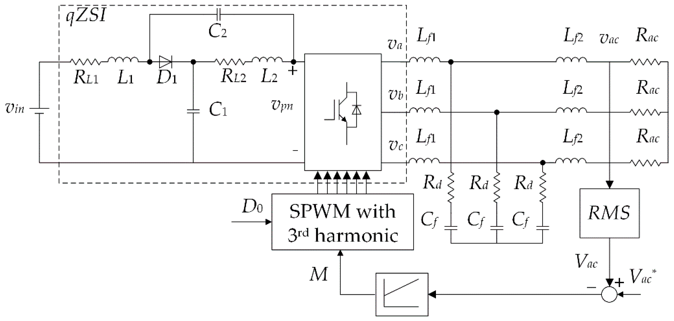
2. Quasi-Z-Source Inverter Power Losses

The considered stand-alone control system with the qZSI is shown in Figure 1. In this study, a symmetrical impedance network is considered, i.e., L1 = L2 = L, C1 = C2 = C, and RL1 = RL2 = RL. The additional LCL filter, composed of the inductors (Lf1, Lf2), capacitors (Cf), and damping resistances (Rd), is connected at the inverter output. The considered qZSI supplies the three-phase resistive load (Rac), whereby the control system maintains the required RMS value of the fundamental load phase voltage (Vac) through adjustment of the modulation index (M). The SPWM with injected 3rd harmonic has been implemented. The qZSI utilizes the standard SPWM switching states (also known as the non-ST states) along with the ST states. The latter occur at the beginning of each zero-switching state of the SPWM, i.e., twice within each switching period (Tsw), in order to provide the required input voltage boost
B = 1 1 2 D = 1 1 2 T 0 T s w
where D is the ST duty cycle and T0 is the ST state period.
The peak value of the load phase voltage (Vac,pk) and the peak value of the inverter bridge input voltage (Vpn) may be defined as follows:
V a c , p k = B M V i n 2 V p n = B V i n = V i n 1 2 D
where Vin represents the qZSI input voltage.
The power losses of the qZSI are defined as the difference between the inverter input and output power. These losses may be divided into the semiconductor losses, the core losses of the impedance network inductors, and the parasitic resistance losses. In this study, the latter losses include only the copper losses of the impedance network inductors, whereas the power losses of the impedance network capacitors are considered negligible due to the low equivalent series resistance (ESR) of the utilized polypropylene capacitors. The parasitic resistance losses of the impedance network inductors were calculated based on the measured inductor current and previously determined parasitic coil resistance, whereas the corresponding core losses were calculated according to the equation proposed by the core manufacturer [23].
The semiconductor losses of the qZSI include the losses of the IGBTs, the FWDs, and the impedance network diode. The losses of the IGBTs include the conduction losses, the switching losses, and the blocking losses. On the other hand, the losses of the diodes include the conduction losses, the reverse recovery losses, and the turn-on losses. The blocking losses of the IGBTs along with the turn-on losses of the diodes may be generally considered negligible. With respect to the above, two novel algorithms for calculation of the qZSI semiconductor losses are proposed in the next section.

3. Proposed Semiconductor LCAs for the Quasi-Z-Source Inverter

In this section, two novel qZSI semiconductor LCAs are presented. Both the proposed LCAs calculate the losses of the IGBTs and FWDs in the three-phase inverter bridge and the losses of the impedance network diode. As for of the inverter bridge, the losses of a single upper IGBT-FWD pair were calculated and then multiplied by six in order to obtain the total bridge losses. The proposed LCAs require the output I–V characteristics of the IGBTs and diodes for calculation of the respective conduction losses, whereas the turn-on (only for the IGBT) and the turn-off characteristics are required for calculation of the respective switching losses. These characteristics are provided in the datasheet of the switching device manufacturer. Figure 2a shows the output I–V characteristics of the utilized IGBT. These characteristics have been linearized by considering the points taken from the datasheet graphs in the low-current range given the fact that the collector current in this study did not exceed 5 A. The IGBT threshold voltage (Vce0) and the IGBT forward resistance (Rce) were extracted for both provided junction temperatures (Tj = 25 °C and Tj = 150 °C). However, with the assumption that the actual junction temperature during normal operation is somewhere between these two values, final values of Vce,0 and Rce were obtained by averaging the values extracted for the two provided temperatures. The I–V characteristics of the FWD and the impedance network diode were approximated in the same way. Finally, the approximated I–V characteristics are defined as follows:
v c e ( i c e ) = V c e , 0 + R c e i c e
v D / D 1 ( i D / D 1 ) = V D / D 1 , 0 + R D / D 1 i D / D 1
where vce and ice are the collector-emitter voltage and the collector current, respectively; vD/D1, VD/D1,0, RD/D1, iD/D1 are the forward voltage, the threshold voltage, the forward resistance, and the forward current of the FWD (subscript “D”) and the impedance network diode (subscript “D1”), respectively.
The values of the threshold voltage and the forward resistance for all the considered semiconductor devices are given in Appendix A.
The datasheets of all the semiconductor devices considered in this paper contain switching energy vs. current characteristics for the junction temperatures Tj = 25 °C and Tj = 150 °C. In addition, these characteristics are provided for the specified reference values of the inverter bridge input voltage (noted as Vref) and the gate resistance. As an example, the IGBT turn-on energy (eTon) vs. the collector current is shown in Figure 2b. The characteristics were extracted for both the provided temperatures and approximated by utilizing the cubic fitting. The coefficients a0on, a1on, a2on, a3on (values given in Appendix A) were obtained by averaging the coefficients determined for the two provided temperatures. In this study, the actual inverter bridge input voltage was different from Vref, so the calculated IGBT turn-on energy was scaled by the ratio ( V p n / V r e f ) k T , according to the recommendations in [22,24], where kT is the exponent representing the voltage dependence of the IGBT switching losses. On the other hand, the value of the gate resistance utilized in the experimental setup corresponded to the value given in the datasheet characteristics of interest. Finally, the same principle of the polynomial coefficient extraction has been applied for the IGBT turn-off characteristic and the reverse recovery characteristics of the qZSI diodes. Thus,
e T o n / o f f ( i c e ) = ( V p n V r e f ) k T ( a 3 o n / o f f i c e 3 + a 2 o n / o f f i c e 2 + a 1 o n / o f f i c e + a 0 o n / o f f )
e D / D 1 r r ( i D ) = ( V p n V r e f ) k D / D 1 ( b 3 D / D 1 i D / D 1 3 + b 2 D / D 1 i D / D 1 2 + b 1 D / D 1 i D / D 1 + b 0 D / D 1 )
where eToff is the turn-off switching energy of the IGBT; eD/D1,rr is the reverse recovery energy of the FWD (subscript “D”) and the impedance network diode (subscript “D1”); kD/D1 is the exponent representing the voltage dependence of the reverse recovery losses.
Values of the polynomial coefficients aoff and bD/D1 are given in Appendix A, whereas Vref of the considered IGBT and diodes is equal to 600 V. Finally, kT = 1.4, kD = kD1 = 0.6 are chosen according to [24].

3.1. Loss-Calculation Algorithm 1

The first LCA is based on the methods which were in [11,12,13] used for the conventional VSI with the SPWM. However, in the considered qZSI configuration, the additional ST states occur, which make the loss calculation more complex.
The conduction losses of a single IGBT are calculated separately for the non-ST state and ST state. In both cases, the conduction losses are calculated based on the conduction energy. The phase current is assumed to be sinusoidal and the current ripple of the impedance network inductor is neglected. The IGBT conduction losses during the non-ST states (PTcond,nST) and the ST states (PTcond,ST) are, respectively, defined as follows (for more details see Appendix B, Equations (A1)–(A9)):
P T c o n d , n S T = V c e , 0 I p h M ( 1 D 2 π + M cos ( φ ) 8 ) + R c e I p h M 2 ( 1 D 8 + M cos ( φ ) 3 π M cos ( 3 φ ) 90 π )
P T c o n d , S T = D [ R c e ( 4 9 I L 2 + 1 8 I p h M 2 ) + V c e , 0 2 3 I L ]
where IphM represents the phase current amplitude, IL represents the mean value of the impedance network inductor current, φ represents the phase angle between the fundamental output phase current and voltage, and M represents the modulation index ( 0 M 2 / 3 ).
The overall conduction losses of all the IGBTs in the three-phase inverter bridge are defined as follows:
P T c o n d = 6 ( P T c o n d , n S T + P T c o n d , S T )
The conduction losses of the FWD are calculated based on its conduction energy. The overall conduction losses of all the FWDs (PDcond) in the three-phase inverter bridge are determined as follows (for more details see Appendix B, Equations (A10)–(A12)):
P D c o n d = 6 [ V D , 0 I p h M ( 1 D 2 π M cos ( φ ) 8 ) + R D I p h M 2 ( 1 D 8 M cos ( φ ) 3 π + M cos ( 3 φ ) 90 π ) ]
The impedance network diode conducts only during the non-ST states, whereby the diode current is assumed to be equal to IL. The corresponding conduction losses are calculated based on the conduction energy. The conduction losses of the impedance network diode are calculated with the assumption that IL is constant within a single Tsw, as follows (for more details see Appendix B, Equation (A13)):
P D 1 c o n d = ( 1 D ) ( R D 1 I L 2 + V D 1 , 0 I L )
The switching losses of the IGBT consist of the switching losses of the non-ST states and the ST states. The switching losses of the non-ST states are caused by the switching transitions between the consecutive non-ST states. These losses may be calculated based on the total number of pulses N which occur within T.
P T o n , n S T = 1 N T n e T o n P T o f f , n S T = 1 N T n e T o f f
where PTon,nST and PToff,nST are the IGBT turn-on and turn-off losses during the switching transitions between the non-ST states, respectively.
The IGBT current is assumed to be sinusoidal during the non-ST states, which implies that the non-ST states switching losses are also sinusoidal. These losses occur only within the positive period of the phase current. By considering the facts mentioned above and switching frequency (fsw), an approximation of Equation (12) can be given as follows:
P T o n , n S T = 1 2 π 0 π f s w e T o n ( I p h M ) sin ( ω t φ ) d ω t = e T o n ( I p h M ) π f s w cos ( φ ) P T o f f , n S T = 1 2 π 0 π f s w e T o f f ( I p h M ) sin ( ω t φ ) d ω t = e T o f f ( I p h M ) π f s w cos ( φ )
The switching losses of the ST states are caused by the switching transitions between the ST state and the non-ST state. The calculation of these losses is a bit more complex. The switching energies during these transitions are determined by the IGBT current during the ST state, which is equal to sum of 1/2 of the phase current and 2/3 of IL. Accordingly, the ST state switching losses may be defined as follows:
P T o n , S T = f s w 2 π 0 2 π [ e T o n ( 2 3 I L ) + e T o n ( I p h M 2 ) sin ( ω t φ ) ] d ω t P T o f f , S T = f s w 2 π 0 2 π [ e T o f f ( 2 3 I L ) + e T o f f ( I p h M 2 ) sin ( ω t φ ) ] d ω t
where PTon,ST and PToff,ST represent the ST states turn-on and turn-off switching losses, respectively.
The ST states switching losses depend on the number of the ST state turn-on and turn-off switching transitions that occur within one Tsw. However, during a single fundamental period of the phase current, this number is not constant. It varies depending on the sign of the phase current and the relation between the instantaneous values of the three reference voltages (vrefA, vrefB, vrefC). For example, the single period of the reference voltage (vrefA) is divided into five intervals, with each interval having a specific constant number of switching transitions within one Tsw. In the intervals where the corresponding phase current (iphA) is negative, the IGBT conducts only during the ST states. Consequently, in these intervals, the ST state turn-on and turn-off switching transitions occur twice within one Tsw. However, in the intervals where iphA > 0, the number of the ST states switching transitions depends on the relation between vrefA, vrefB, and vrefC, due to the occurrence of the non-ST switching transitions at the intersection points of vrefA and the carrier triangular signal. The borders of these intervals are defined by the time points where vrefA intersects the remaining two reference voltages, and also by the time points of iphA zero crossings.
There are two separate set of equations for the calculation of the ST states switching losses. The first set applies for the phase angles between 0 and π/6 (case 1), whereas the second set applies for the phase angles between π/6 and π/2 (case 2). Table 1 and Table 2 show the number of switching transitions in the defined intervals for the cases 1 and 2, respectively. The number of switching transitions given in the considered tables is defined based on Figure 3, where the period equal to ωTsw is magnified within each considered phase angle interval. The labels a, b, c, d, e (a’, b’, c’, d’, e’) represent only the part of the intervals I1, I2, I3, I4, I5 (I1, I2, I3, I4, I5,), respectively, with the length equal to ωTsw.
In the case 1, shown in Figure 3a, the IGBT turns on straight into the ST state (NST,on) and turns off from the ST state (NST,off) twice during each Tsw in the intervals I1 and I5. In the intervals I2 and I4, both the ST switching transitions occur once during each Tsw, as well as the IGBT turn-on (NnST,on) and turn-off (NnST,off) transitions into non-ST states. On the other hand, in the interval I3, the ST state occurs when the IGBT is already conducting, so there are no switching transitions (NnST,off = 0 and NST,on = 0). Since the phase current is positive and the turn-off switching losses between non-ST states are already obtained from Equation (13), their influence has to be eliminated from the switching loss equations defined for the interval I3. The ST states switching losses for the case 1 are calculated based on the number of switching transitions defined in Table 1 and Equation (14), as follows (for more details see Appendix C, Equation (A14)):
P T o n , S T = f s w [ 7 6 e T o n ( 2 3 I L ) 3 cos ( φ ) + 2 2 π e T o n ( I p h M 2 ) ] P T o f f , S T = f s w [ 3 2 e T o f f ( 2 3 I L ) 1 π e T o f f ( I p h M 2 ) 3 cos ( φ ) 2 π e T o f f ( I p h M ) ]
In the case 2, when φ is in between π/6 and π/2, the number of the switching transitions defined in Table 2 is determined based on Figure 3b. The ST states switching losses for the case 2 are calculated based on the number of switching transitions defined in Table 2 and Equation (14), as follows (for more details see Appendix C, Equation (A15)):
P T o n , S T = f s w [ ( 1 + φ π ) e T o n ( 2 3 I L ) 3 cos ( φ ) + 2 2 π e T o n ( I p h M 2 ) e T o n ( I p h M ) 1 cos ( φ π / 6 ) 2 π ] P T o f f , S T = f s w [ 3 2 e T o f f ( 2 3 I L ) 1 π e T o f f ( I p h M 2 ) cos ( φ + π / 6 ) + 1 2 π e T o f f ( I p h M ) ]
The overall switching losses of the IGBTs in the three-phase inverter bridge are defined as follows:
P T s w = 6 ( P T o n , n S T + P T o f f , n S T + P T o n , S T + P T o f f , S T )
The FWD conducts only the phase current, so the reverse recovery losses of the diode are also sinusoidal. The overall reverse recovery losses of all six FWDs (PDrr) in the three-phase inverter bridge are determined as follows:
P D r r = 6 f s w 2 π 0 π e D r r ( I p h M ) sin ( ω t φ ) d ω t = 6 f s w 2 π 0 π J d ω t
The number of the reverse recovery switching transitions of the FWD is closely related to the IGBT turn-on switching transitions; namely, every time the IGBT turns on during the positive period of the phase current, the FWD recovers. That means that the total number of the diode reverse recoveries, in fact, equals the sum of the IGBT turn-on switching transitions (NnST,on + NST,on) during the positive period of the phase current. Consequently, the reverse recovery losses of the FWDs have been calculated by considering the cases defined above. In case 1, based on Table 1 and Equation (18), PDrr are defined as follows:
P D r r = 6 f s w 2 π [ 2 φ π 6 J d ω t + π 6 5 π 6 J d ω t + 2 5 π 6 ( φ + π ) J d ω t ] = 6 f s w 4 3 cos ( φ ) 2 π e D r r ( I p h M )
In the case 2, based on Table 2 and Equation (18), PDrr are defined as follows:
P D r r = 6 f s w 2 π [ φ 5 π 6 J d ω t + 2 5 π 6 7 π 6 J d ω t + 2 7 π 6 ( φ + π ) J d ω t ] = 6 f s w sin ( φ ) 3 cos ( φ ) + 6 4 π e D r r ( I p h M )
It is important to note that for the boundary phase angle of π/6, Equations (15) and (16) become equal, as well as Equations (19) and (20). Thus, the switching losses are changing continuously with the phase angle.
The impedance network diode recovers every time the ST state occurs, i.e., twice during each Tsw. With the reverse recovery current being considered equal to IL, the reverse recovery losses of the impedance network diode are defined as follows:
P D 1 r r = 2 f s w e D 1 r r ( I L )

3.2. Loss-Calculation Algorithm 2

The second LCA is based on the algorithm presented in [20,21], which is for the first time here adapted for the qZSI. The corresponding flow chart is shown in Figure 4. The semiconductor losses are calculated by considering the instantaneous values of the following variables in kth and (k − 1)st instants: the ST state signal (STsignal), the non-ST state switching pulses of the IGBT (p), the phase current (iph), the impedance network diode current (iD1), the impedance network inductor current (iL), and the input voltage of the inverter (vin).
The calculation of the IGBT conduction energy (eTcond) requires the value of the collector current. This current is equal to the phase current (iph) during the non-ST states. However, during the ST states, it is equal to the sum of one half of the phase current and two thirds of the impedance network inductor current. The IGBT conduction energy is calculated as follows:
e T c o n d ( k ) = e T c o n d ( k 1 ) + v c e ( k ) | i c e ( k ) | [ t ( k ) t ( k 1 ) ] v c e ( k ) = V c e , 0 + R c e | i c e ( k ) |
The FWD does not conduct during the ST state, whereas it conducts part of the phase current during the negative half-period. The FWD conduction energy is defined as follows:
e D c o n d ( k ) = e D c o n d ( k 1 ) + v D ( k ) | i p h ( k ) | [ t ( k ) t ( k 1 ) ] v D ( k ) = V D , 0 + R D | i p h ( k ) |
Further, the turn-on (eTon) and the turn-off (eToff) switching energies of the IGBT are calculated based on the collector current, whereas the reverse recovery energy (eDrr) of the FWD is calculated based on the phase current as follows:
e T o n / o f f ( k ) = e T o n / o f f ( k 1 ) + e T o n / o f f ( | i c e ( k ) | )
e D r r ( k ) = e D r r ( k 1 ) + e D r r ( | i p h ( k ) | )
The conduction energy (eD1cond) and reverse recovery energy (eD1rr) of the impedance network diode are calculated as follows:
e D 1 c o n d ( k ) = e D 1 c o n d ( k 1 ) + v D 1 ( k ) | i D 1 ( k ) | [ t ( k ) t ( k 1 ) ] v D 1 ( k ) = V D 1 , 0 + R D 1 | i D 1 ( k ) | e D 1 r r ( k ) = e D 1 r r ( k 1 ) + e D 1 r r ( | i D 1 ( k ) | )
Finally, the calculation of the corresponding power losses requires dividing of the energies accumulated in the time window (tw), corresponding to the integer number of cycles of the phase current, with the time window duration in seconds.

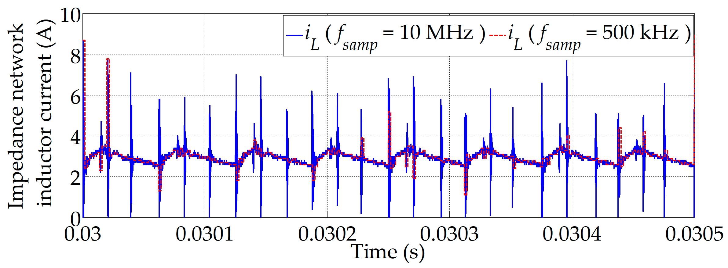
4. Experimental Testing and Evaluation

The laboratory setup of the system shown in Figure 1 was built in order to test the proposed LCAs. The qZSI was supplied by the dc power supply Chroma 62050H-600S which provides voltages up to 600 V and currents up to 8.2 A. The three-phase inverter bridge is composed of six IGBTs with integrated FWDs IRG8P60N120KD (International Rectifier). The gate drivers SKHI 22B(R) (Semikron) were utilized to drive the IGBTs. The impedance network diode was built as a parallel compound of four FWDs of the IGBT-FWD pair IRG8P25N120KD (International Rectifier) since the impedance network current would be too excessive for a single diode of this type. The parameters of the inductors and capacitors in the impedance network along with the LCL filter parameters are given in Appendix D. The control algorithm was implemented by means of the MicroLabBox (dSpace) microcontroller and executed with the sampling frequency of 10 kHz. The reference RMS value and frequency of the fundamental load phase voltage were set to 230 V and 50 Hz, respectively. The ST signals were injected by a hardware circuit placed in between the digital outputs of the MicroLabBox and the signal inputs of the gate drivers.

4.1. Implementation Requirements of the Proposed Loss-Calculation Algorithms

Implementation requirements represent the important factor in the analysis of the proposed LCAs. They include the computational requirements, the number of required input variables and parameters, and the number of additional current/voltage sensors required to implement the desired LCA. The common input variables of the proposed algorithms are D, iL, Vin, and iph. The additional input parameters of the LCA1 are M and φ, whereas in the case of the LCA2, the additional input signals are the iD1 waveform, the ST state signal, and the non-ST state switching pulses.
The value of the duty cycle required for the implementation of the LCA2 was obtained from the control algorithm. On the other hand, the currents required for the implementation of the LCA2 (iL, iph, iD1) were measured by means of the Hall-effect transducers IT 60-S (LEM). The input voltage of the qZSI, also required for the implementation of the LCA 2, has been measured by means of the Hall effect transducers CV 3–500 (LEM).
The waveforms of the three input currents (iL, iph, iD1) and the non-ST state switching pulses of the IGBT, required by the LCA2, were recorded by the oscilloscope MDO 3014 (Tektronix), which ensures sampling frequencies (fsamp) up to 10 MHz. The waveform of the qZSI input voltage was recorded by the oscilloscope SDS 1104X-E (Siglent), whereas the ST state signal was reconstructed based on the iD1 waveform, as shown in Figure 5. During the ST states (STsignal = 1), iD1 is zero, whereas during the non-ST states (STsignal = 0), this current is always positive.
The signals acquired by the oscilloscope MDO 3014 were originally sampled at 10 MHz and subsequently downsampled to determine the minimum value of fsamp that still allows capturing the required information from the recorded waveforms. With regard to this, the waveforms of iD1 and STsignal were analyzed for the highest switching frequency considered in this study, which is 8 kHz. The minimum sufficient fsamp obtained for this case is also sufficient for switching frequencies lower than 8 kHz because lower fsw implies lower minimum fsamp. During the measurement of the waveforms shown in Figure 5, the ST duty cycle was 0.22, which along with fsw = 8 kHz, according to Equation (1), determines the ST state duration T0/2 = 13.75 μs. For fsamp = 10 MHz (Figure 5a), the measured duration of each ST state (T0/2) deviated by about ± 0.7 μs from the mentioned calculated value. This deviation is a consequence of an error induced by the hardware circuit that injects the ST signals. The goal was to retain approximately the same deviation of T0/2 value while reducing fsamp. The minimum fsamp value for which this was achieved was equal to 500 kHz (Figure 5b). For the sampling frequencies lower than 500 kHz, the iD1 waveform could not be any more faithfully reconstructed, which led to an error in T0/2 value of up to 3 μs.
The impedance network inductor current waveform shown in Figure 6 was also sampled with the frequency of fsamp = 500 kHz, although this signal could be faithfully reconstructed by applying the sampling frequency as low as 100 kHz. However, it is mandatory for the non-ST state switching pulses of the IGBT to be sampled with the same frequency as the waveform of iD1 in order to avoid the mismatch between that signal and the reconstructed ST state signal. Finally, the waveforms of the phase current and the qZSI input voltage were sampled with 10 kHz.
The LCA1 requires the values of M, D, φ, IL, Vin, and IphM for implementation. The latter three values may be relatively easily determined from the measured waveforms, whereas the values of M and D are obtained from the control algorithm. However, the value of φ has to be either determined from the measured phase current and voltage or known in advance (e.g., for a resistive load, φ = 0).
It may be concluded that the implementation of the LCA2 is more complex primarily due to an additional current sensor required for iD1. Moreover, all three additional input signals required by the LCA2 have to be sampled with high sampling frequencies (i.e., 500 kHz or higher for the setup used in this study).

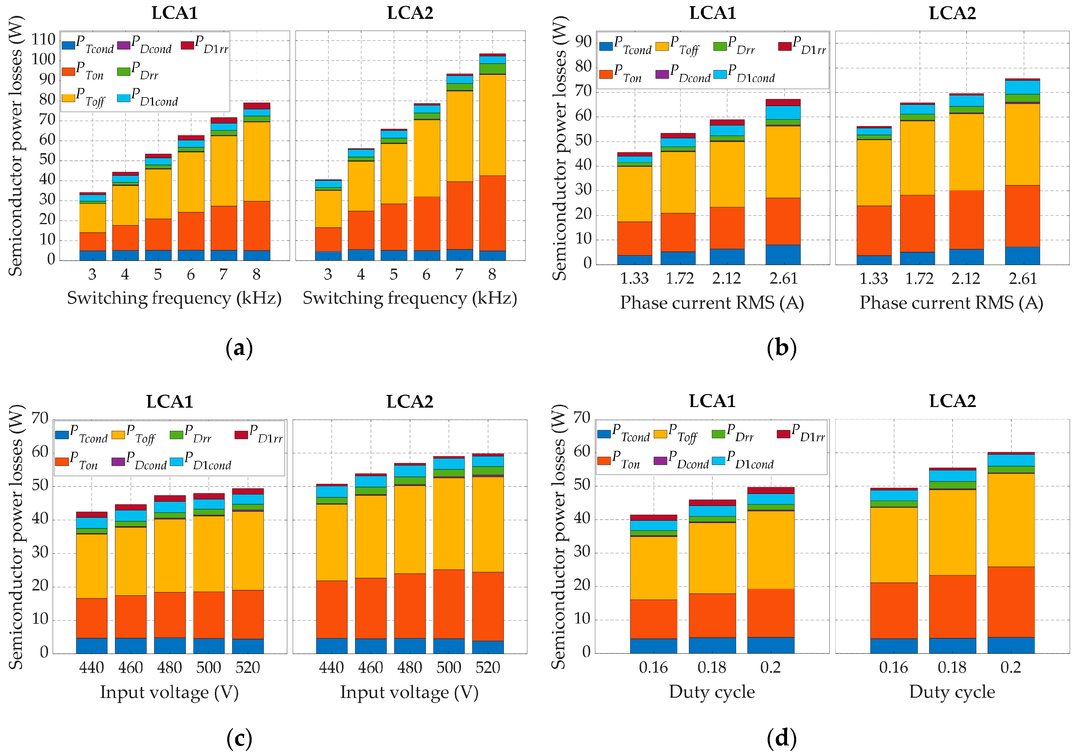
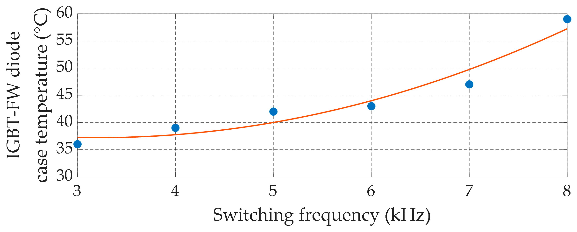
4.2. Experimental Results

All the experiments were carried out with the three-phase resistive load (φ = 0) connected to the inverter output. Figure 7 shows the semiconductor power losses distribution with respect to the switching frequency, RMS value of the phase current, qZSI input voltage, and duty cycle. During the variation of the switching frequency, the other system parameters were D = 0.22, Iph = 1.72 A, Vin = 450 V, whereas the variation of Iph, Vin, and D was carried out with the switching frequency set to 5 kHz. Different RMS values of the phase current were achieved by varying the load resistance, with D = 0.22 and Vin = 450 V. The variation of the input voltage was carried out with D = 0.18 and Iph = 1.72 A, whereas the variation of the duty cycle was carried out with Vin = 470 V and Iph = 1.72 A. The selected ranges of Vin and D were determined by considering several limitations of the utilized laboratory setup; namely, the combination of high input voltage and high ST duty cycle may result in IGBT collector-emitter voltage higher than the allowed maximum value of 1200 V, which may ultimately destroy the device. On the other hand, too low an input voltage would require a higher than allowed modulation index, whose value, according to the maximum constant boost strategy, must not exceed 2 / 3 ( 1 D ) in order to maintain the six active states of the inverter intact [4]. Finally, high input voltage in combination with high duty cycle may cause the electromagnetic interference, which may disrupt the normal operation of the gate drivers.
The increase of the semiconductor losses with all four varied parameters was noted for both the proposed algorithms. However, arguably the largest increase is noted with the increase of the switching frequency. For example, at fsw = 3 kHz, the total semiconductor losses calculated by the LCA1 and LCA2 amounted to PLCA1 = 34 W and PLCA2 = 40 W, respectively, whereas at fsw = 8 kHz, these values have more than doubled and amounted to PLCA1 = 79 W and PLCA2 = 103 W, respectively. On the other hand, a less pronounced change in the semiconductor losses was noted in the considered ranges of the phase current, the input voltage, and the duty cycle.
Both algorithms indicate that the total losses of the IGBTs, considered as the sum of the respective switching and conduction losses, are dominant compared to the total diode losses and account for approximately 87% of the total semiconductor losses. In addition, the IGBT conduction losses account for approximately 10% of the total IGBT losses for both the algorithms. These losses are practically unaffected by the switching frequency and duty cycle since the IGBT current remains the same with the variation of these two parameters. However, the conduction losses increase with the phase current, whereas they decrease with the input voltage due to the decrease of the qZSI input current for the same applied load. The IGBT switching losses, which account for approximately 90% of the total IGBT losses, consist of the turn-on (PTon) and turn-off (PToff) switching losses. These losses significantly increase with the switching frequency due to the increase of the number of switching transitions. The same tendency is noted with the increase of the phase current due to the increase of switching energies according to Equation (5). The switching losses of the IGBTs also increase with the duty cycle and the input voltage due to the increase of Vpn as per Equation (2). The total losses of the FWDs account for approximately 5% of the total semiconductor losses, where the reverse recovery losses are dominant over the conduction losses. Finally, the remaining 8% of the total semiconductor losses belong to the impedance network diode losses, with the conduction losses being dominant over the reverse recovery losses. The mentioned losses of the qZSI’s diodes have similar behavior as the losses of the IGBTs in terms of variation with fsw, iph, Vin, and D.
The semiconductor losses calculated by the two proposed LCAs have been compared with the measured ones. For that purpose, the input and output inverter power along with the power losses of the impedance network inductors (PL) and capacitors had to be obtained. As in [25], the copper losses of the impedance network inductors were calculated based on the respective current and the parasitic coil resistance. Likewise, the inductors’ core losses were calculated according to the equation proposed in the datasheet of the core manufacturer [23]. The same datasheet shows that the losses of this core type are practically unaffected by the core temperature in the case of a continuous operation of up to 10 h, regardless of the values of the switching frequency and the magnetic induction. Since the experiments in this study lasted less than one hour, the temperature impact was neglected. The power losses of the impedance network capacitors were neglected due to the low ESR value. The inverter input power Pin was obtained as the mean value of iLvin, whereas the inverter output power (Pacinv) was measured by the high-precision power analyzer Norma 4000 (Fluke). The semiconductor losses were ultimately obtained as PinPacinvPL, with the wire parasitic resistance losses considered negligible.
Figure 8 shows the comparison between the measured semiconductor losses (Pmeasured) and the calculated semiconductor losses from Figure 7. The absolute errors of both the LCA1 and LCA2 increase significantly with the switching frequency as shown in Table 3. On the other hand, the absolute errors of the proposed algorithms only slightly increase with the phase current RMS value, qZSI input voltage and duty cycle. Overall, the LCA2 provided more accurate results for all the considered values of fsw, iph, Vin, and D. By assuming that the inductor core losses are calculated accurately, that the capacitor losses are negligible, and that both the input and output power of the inverter are accurately measured, the remaining differences between the measured and calculated losses are ascribed to the LCA errors. The errors of both the proposed LCAs significantly increase with the switching frequency. It is suspected that the values of the switching energies in the considered laboratory setup were higher than the values provided in the datasheet of the IGBT manufacturer, which are determined based on the double-pulse test. This is, presumably, due to the shortcomings of the double-pulse test such as errors in the calculation of switching energies due to inaccuracies in voltage/current measurement or the influence of the parasitic capacitances and additional loop inductance/resistance within the test circuitry on the switching energies, as described in [26].
The influence of the switching frequency on the switching losses may be shown by considering the temperature of the semiconductor device. For that purpose, the IGBT-FWD case temperature was measured in steady state by means of the thermal camera Testo 865 (Testo) for all the considered switching frequencies. Figure 9 shows that, for the frequency increase from 3 kHz to 7 kHz, the IGBT-PWD case temperature increased by a total of 11 °C. However, when the switching frequency was increased from 7 kHz to 8 kHz, the temperature increased for 12 °C. These results confirm that the IGBT-FWD switching losses significantly increase with the switching frequency since the conduction losses are not affected by the switching frequency. The temperature increase is presumably caused by the increase of the IGBT switching losses, since both the proposed algorithms indicate that they are dominant over the FWD switching losses.

4.2.1. Correction of the IGBT Switching Losses Calculation

As a way of simple correction of the calculated IGBT switching losses, the IGBT turn-on and turn-off switching energies defined in Equation (5) were multiplied by the same factor greater than 1 with the aim of reducing the LCA2 error to zero. The LCA2 was chosen for the correction because it involves far less simplifications compared to the LCA1 so it, expectedly, provided more accurate results prior to the correction. The final value of the multiplication factor was determined by averaging the values obtained for several measurement points. For that purpose, four points with the Iph values of 1.33 A, 1.72 A, 2.12 A, and 2.61 A were chosen. For all the considered points, the switching frequency was set to 5 kHz and Vpn amounted to 800 V, thus maintaining the constant Vpn/Vref ratio. Hence, the influence of kT was the same for all the considered measurement points. The value of the average multiplication factor obtained in this manner is 1.53, which implies 53% higher IGBT switching energies. Note that by applying the multiplication factor in the described manner, all the other remaining errors, such as the input/output power measurement errors, are ascribed as the calculation error of the IGBT switching losses. Ultimately, the same value of the corrective multiplication factor was applied for both the LCAs.
Figure 8 shows the comparison between the proposed LCAs-prior and after the correction of the IGBT switching energies- and the measured semiconductor losses. In Table 3, the absolute and relative errors are given with respect to the measured semiconductor losses for all the considered fsw values. The accuracy of the LCAs notably increased after the correction of the IGBT switching energies. The same tendency is noted with regard to the qZSI input voltage, the phase current, and the duty cycle.

4.2.2. Efficiency and Semiconductor Losses Share of the qZSI

Figure 10 shows the qZSI efficiency and the share of the measured semiconductor losses in the total inverter losses with respect to the switching frequency. The inverter efficiency decreases approximately linearly in the considered frequency interval, whereas the share of the measured semiconductor losses increases rapidly from about 50% at fsw = 3 kHz to almost 85% at fsw = 8 kHz.

5. Conclusions

This paper presents two novel semiconductor LCAs for the three-phase qZSI. The proposed LCAs were successfully applied for the considered inverter in the stand-alone operation mode. However, the proposed algorithms are also applicable for different control systems as well as for grid-tied applications. Both the proposed LCAs indicate that the losses of the transistors are dominant and account for approximately 87% of all the semiconductor losses. Of all transistor losses, the switching losses are dominant with the percentage of 90%. The differences noted between the measured and calculated semiconductor losses are, presumably, due to the differences between the actual switching energies and those provided in the datasheet of the transistor manufacturer. Therefore, the transistor datasheet switching energies, which were used as the input data for the LCAs, were multiplied by the experimentally determined factor of 1.53, which resulted in the mean absolute percentage errors of 11.2% and 7.9% for the LCA1 and LCA2, respectively. Alternatively, instead of relying on the manufacturers characteristics, more accurate IGBT switching characteristics may be obtained prior to LCAs implementation (e.g., determined experimentally from the measurements taken in the normal operating conditions of the considered qZSI) and then used as the input data for the LCAs, and even scaled with respect to the actual measured IGBT case temperature. The experimental results indicate that the qZSI semiconductor losses significantly drop with the switching frequency, resulting in better inverter efficiency. On the other hand, the total harmonic distortion value of the phase currents increases at lower switching frequencies, thus making filter design a more demanding task.

Author Contributions

Conceptualization, I.G., D.V. and M.B. (Mateo Bašić); methodology, I.G. and D.V.; software, I.G. and M.B. (Matija Bubalo); validation, I.G.; formal analysis, I.G.; investigation, I.G.; resources, D.V.; data curation, I.G.; writing—original draft preparation, I.G.; writing—review and editing, D.V. and M.B. (Mateo Bašić); visualization, I.G.; supervision, D.V.; project administration, D.V.; funding acquisition, D.V. All authors have read and agreed to the published version of the manuscript.

Funding

This work has been fully supported by Croatian Science Foundation under the project (IP-2016-06-3319).

Conflicts of Interest

The authors declare no conflict of interest.

Appendix A

Polynomial coefficients in Equations (3)–(6)
  • Rce = 0.066105 Ω, Vce,0 = 0.6823 V
  • RD = 0.0862 Ω, VD,0 = 0.774 V
  • RD1 = 0.1225 Ω, VD1,0 = 0.999 V
  • a0on = 0.18, a1on = 0.074, a2on = −7.2 × 10⁻⁴, a3on = 2.537 × 10⁻⁵
  • a0off = 0.258, a1off = 0.081, a2off = −1.41 × 10⁻⁴, a3off = 0
  • b0D = 0.036, b1D = 0.04, b2D = −3.76 × 10⁻⁴, b3D = 9.9 × 10⁻⁷
  • b0D1 = 0.0145, b1D1 = 0.052, b2D1 = −0.0012, b3D1 = 5.34 × 10⁻⁶

Appendix B

The conduction energy of the IGBT during the non-ST states within one Tsw are given by
E T c o n d , n S T = v c e i c e , n S T d T , n S T T s w
where ice,nST = IphM sin (ωt), dT,nST represents the IGBT duty cycle during the non-ST states, which is, in turn, defined as follows:
d T , n S T = 1 2 { 1 + M [ sin ( ω t + φ ) + 1 6 sin [ 3 ( ω t + φ ) ] ] } D 2
The first term in Equation (A2) represents the duty cycle in the case when the traditional SPWM with the injected 3rd harmonic is implemented. The factor –D/2 appears in Equation (A2) in order to eliminate the impact of the corresponding ST state (Figure 3a, lower right corner). By substituting Equations (3) and (A2) in Equation (A1), it becomes
E T c o n d , n S T = ( R c e I p h M sin ( ω t ) + V c e 0 ) I p h M sin ( ω t ) { 1 2 { 1 + M [ sin ( ω t + φ ) + 1 6 sin [ 3 ( ω t + φ ) ] ] } D 2 } T s w
Based on the differential form of Equation (A3) (Tsw = dt = T/2π dωt), the IGBT conduction losses that occur during the non-ST states are defined as follows:
P T c o n d , n S T = 1 T 0 T / 2 d E T c o n d , n S T = 1 2 π 0 π E T c o n d , n S T d ω t
By substituting Equation (A3) into Equation (A4), PTcond,nST are defined as follows:
P T c o n d , n S T = I p h M 4 π 0 π ( R c e I p h M sin ( ω t ) + V c e , 0 ) sin ( ω t ) { 1 D + M [ sin ( ω t + φ ) + 1 6 sin [ 3 ( ω t + φ ) ] ] } d ω t
The final expression of PTcond,nST is obtained by solving the integral on the right-hand side of Equation (A5).
The conduction energy of the IGBT during the ST states within one Tsw is given by
E T c o n d , S T = v c e i c e , S T D T s w
The IGBT current during the ST state may be approximated as follows [14]:
i c e , S T = 2 3 I L + 1 2 I p h M sin ( ω t )
By substituting Equations (3) and (A7) in Equation (A6), it becomes
E T c o n d , S T = [ R c e ( 2 3 I L + 1 2 I p h M sin ( ω t ) ) + V c e , 0 ] ( 2 3 I L + 1 2 I p h M sin ( ω t ) ) D T s w
Based on the differential form of Equation (A8) (Tsw = dt = T/2π dωt), the IGBT conduction losses that occur during the ST states are defined as follows:
P T c o n d , S T = 1 2 π 0 2 π [ R c e ( 2 3 I L + 1 2 I p h M sin ( ω t ) ) + V c e , 0 ] ( 2 3 I L + 1 2 I p h M sin ( ω t ) ) D d ω t
The final expression of PTcond,ST is obtained by solving the integral on the right-hand side of Equation (A9).
The conduction energy of the FWD within one Tsw is defined as follows:
E D c o n d = i c e , n S T v D ( 1 d T , n S T D ) T s w = v D d D T s w i c e , n S T
where the FWD current is assumed to be sinusoidal, whereas the diode duty cycle (dD) is defined according to the dT,nST and D, as follows:
d D = 1 2 { 1 M [ sin ( ω t + φ ) + 1 6 sin [ 3 ( ω t + φ ) ] ] } D 2
By substituting Equations (4) and (A11) into Equation (A10), it becomes
E D c o n d = ( R D I p h M sin ( ω t ) + V D , 0 ) I p h M sin ( ω t ) { 1 2 { 1 M [ sin ( ω t + φ ) + 1 6 sin [ 3 ( ω t + φ ) ] ] } D 2 } T s w
The FWD conduction losses (PDcond) were calculated as the integral of the differential form of Equation (A12), similarly as the IGBT conduction losses.
The impedance network diode conduction energy within one Tsw is defined as follows:
E D 1 c o n d = ( R D 1 I L + V D 1 , 0 ) I L ( 1 D ) T s w

Appendix C

Calculation of the switching losses in LCA1 for 0 < φ < π/6
P T o n , S T = f s w 2 π [ 2 0 φ K d ω t + φ π 6 K d ω t + 5 π 6 ( π + φ ) K d ω t + 2 ( π + φ ) 2 π K d ω t ] P T o f f , S T = f s w 2 π [ 2 0 φ I d ω t + φ π 6 I d ω t + π 6 5 π 6 I d ω t + 5 π 6 ( π + φ ) I d ω t + 2 ( π + φ ) 2 π I d ω t π 6 5 π 6 e o f f ( I p h M ) sin ( ω t φ ) d ω t ]
Calculation of the switching losses in LCA1 for π/6 < φ < π/2
P T o n , S T = f s w 2 π [ 2 0 φ K d ω t + 5 π 6 7 π 6 K d ω t + 2 7 π 6 ( π + φ ) K d ω t + 2 ( π + φ ) 2 π K d ω t 7 π 6 ( π + φ ) e T o n ( I p h M ) sin ( ω t φ ) d ω t ] P T o f f , S T = f s w 2 π [ 2 0 φ I d ω t + φ 5 π 6 I d ω t + 5 π 6 7 π 6 I d ω t + 7 π 6 ( π + φ ) I d ω t + 2 ( π + φ ) 2 π I d ω t φ 5 π 6 e T o f f ( I p h M ) sin ( ω t φ ) d ω t ]
where K = eTon (2/3IL) + eTon (IphM/2) sin(ωt − φ), I = eToff (2/3IL) + eToff (IphM/2) sin(ωt − φ)

Appendix D

Parameters of the impedance network inductors:
T520-26 powder cores (Micrometals), L = 20.2 mH (unsaturated), and RL = 0.5 Ω (at 25 °C).
Parameters of the impedance network capacitors:
MKSPI35-50U/1000 polypropylene capacitors (Miflex), C = 50 μF, and ESR = 7.8 mΩ.
Parameters of the output LCL filter:
Lf1 = 8.64 mH, Lf2 = 4.32 mH, Cf = 4 μF, and Rd = 10 Ω.

References

  1. Peng, F.Z. Z-source inverter. IEEE Trans. Ind. Appl. 2003, 39, 504–510. [Google Scholar] [CrossRef]
  2. Ellabban, O.; Abu-Rub, H. Z-source inverter: Topology improvements review. IEEE Ind. Electron. 2016, 10, 6–24. [Google Scholar] [CrossRef]
  3. Siwakoti, Y.P.; Peng, F.Z.; Blaabjerg, F.; Loh, F.C.; Town, G.E. Impedance-source networks for electric power conversion part I: A topological review. IEEE Trans. Power Electr. 2015, 30, 699–716. [Google Scholar] [CrossRef]
  4. Siwakoti, Y.P.; Peng, F.Z.; Blaabjerg, F.; Loh, F.C.; Town, G.E.; Yang, S. Impedance-source networks for electric power conversion part II: Review of control and modulation techniques. IEEE Trans. Power Electr. 2015, 30, 1887–1906. [Google Scholar] [CrossRef]
  5. Anderson, J.; Peng, F.Z. Four quasi-Z-source inverters. In Proceedings of the 2008 IEEE Power Electronics Specialists Conference, Rhodes, Greece, 15–19 June 2008. [Google Scholar] [CrossRef]
  6. Franke, W.T.; Mohr, M.; Fuchs, F.W. Comparison of a Z-Source inverter and a voltage-source inverter linked with a DC/DC-boost-converter for wind turbines concerning their efficiency and installed semiconductor power. In Proceedings of the 2008 IEEE Power Electronics Specialists Conference, Rhodes, Greece, 15–19 June 2008. [Google Scholar] [CrossRef]
  7. Noroozi, N.; Yaghoubi, M.; Zolghadri, M.R. A modulation method for leakage current reduction in a three-phase grid-tie quasi-Z-source inverter. IEEE Trans. Power Electr. 2019, 34, 5439–5450. [Google Scholar] [CrossRef]
  8. Cauffet, G.; Keradec, J.P. Digital oscilloscope measurements in high-frequency switching power electronics. IEEE Trans. Instrum. Meas. 1992, 41, 856–860. [Google Scholar] [CrossRef]
  9. Tektronix. Measuring Power Supply Switching Loss with an Oscilloscope, 1st ed.; Tektronix: Beaverton, OR, USA, 2016. [Google Scholar]
  10. Iijima, R.; Isobe, T.; Tadano, H. Loss analysis of Z-source inverter using SiC-MOSFET from the perspective of current path in shoot-through mode. In Proceedings of the 18th European Conference on Power Electronics and Applications, Karlsruhe, Germany, 5–9 September 2016. [Google Scholar] [CrossRef]
  11. Casanellas, F. Losses in PWM inverters using IGBTs. IEE P.-Elect. Pow. Appl. 1994, 141, 235–239. [Google Scholar] [CrossRef]
  12. Berringer, K.; Marvin, J.; Perruchoud, P. Semiconductor power losses in ac inverters. In Proceedings of the IEEE Industry Applications Conference, Orlando, FL, USA, 8–12 October 1995. [Google Scholar] [CrossRef]
  13. Bierhoff, M.H.; Fuchs, F.W. Semiconductor losses in voltage source and current source IGBT converters based on analytical derivation. In Proceedings of the IEEE 35th Annual Power Electronics Specialists Conference, Aachen, Germany, 20–25 June 2004. [Google Scholar] [CrossRef]
  14. Shen, M.; Joseph, A.; Wang, J.; Peng, F.Z.; Adams, D.J. Comparison of traditional inverters and Z-source inverter for fuel cell vehicles. IEEE Trans. Power Electr. 2007, 22, 1453–1463. [Google Scholar] [CrossRef]
  15. Shen, M.; Joseph, A.; Huang, Y.; Peng, F.Z.; Qian, Z. Design and development of a 50kW Z-source inverter for fuel cell vehicles. In Proceedings of the CES/IEEE 5th International Power Electronics and Motion Control Conference, Shanghai, China, 14–16 August 2006. [Google Scholar] [CrossRef]
  16. Battiston, A.; Martin, J.; Miliani, E.; Nahid-Mobarakeh, B.; Pierfederici, S.; Meibody-Tabar, F. Comparison criteria for electric traction systems using Z-source/quasi Z-source inverter and conventional architectures. IEEE J. Em. Sel. Top. P. 2014, 2, 467–476. [Google Scholar] [CrossRef]
  17. Lei, Q.; Peng, F.Z.; He, L.; Yang, S. Power loss analysis of current-fed quasi-Z-source inverter. In Proceedings of the IEEE Energy Conversion Congress and Exposition (ECCE 2010), Atlanta, GA, USA, 12–16 September 2010. [Google Scholar] [CrossRef]
  18. Zdanowski, M.; Peftitsis, D.; Piasecki, S.; Rabkowski, J. On the design process of a 6-kVA quasi-Z-inverter employing SiC power devices. IEEE Trans. Power Electr. 2016, 31, 7499–7508. [Google Scholar] [CrossRef]
  19. Abdelhakim, A.; Davari, P.; Blaabjerg, F.; Mattavelli, P. Switching loss reduction in three-phase quasi-Z-source inverters utilizing modified space vector modulation strategies. IEEE Trans. Power Electr. 2017, 33, 4045–4060. [Google Scholar] [CrossRef]
  20. Bazzi, A.M.; Kimball, J.W.; Kepley, K.; Krein, P.T. A simple analysis tool for estimating power losses in an IGBT-diode pair under hysteresis control in three-phase inverters. In Proceedings of the Twenty-Four Annual IEEE Applied Power Electronics Conference and Exposition, Washington, DC, USA, 15–19 February 2009. [Google Scholar] [CrossRef]
  21. Bazzi, A.M.; Krein, P.T.; Kimball, J.W.; Kepley, K. IGBT and diode loss estimation under hysteresis switching. IEEE Trans. Power Electron. 2012, 27, 1044–1048. [Google Scholar] [CrossRef]
  22. Ivakhno, V.; Zamaruiev, V.; Ilina, O. Estimation of semiconductor switching losses under hard switching using Matlab/Simulink subsystem. Electr. Control Commun. Eng. 2013, 2, 20–26. [Google Scholar] [CrossRef]
  23. Micrometals. Power conversion and line filter application; Issue, L., Ed.; Micrometals Inc.: Anaheim, CA, USA, 2007. [Google Scholar]
  24. Semikron. Application Manual Power Semiconductors, 2nd ed.; ISLE Verlag: Ilmenau, Germany, 2015. [Google Scholar]
  25. Grgić, I.; Bubalo, M.; Vukadinović, D.; Bašić, M. Power losses analysis of a three-phase quasi-Z-source inverter. In Proceedings of the 5th International Conference on Smart and Sustainable Technologies, Split, Croatia, 23–26 September 2020. [Google Scholar]
  26. Cougo, B.; Schneider, H.; Meynard, T. Accurate switching energy estimation of wide bandgap devices used in converters for aircraft applications. In Proceedings of the 15th European Conference on Power Electronics and Applications, Lille, France, 2–6 September 2013. [Google Scholar] [CrossRef]
Figure 1. Control system of the qZSI in a stand-alone operation mode.
Electronics 09 01642 g001
Figure 2. I–V characteristics (a) and turn-on characteristics (b) of the utilized IGBT.
Electronics 09 01642 g002
Figure 3. Waveforms of the reference voltages, the carrier triangular signal, and the IGBT current for the phase angle between 0 and π/6 (a) and the phase angle between π/6 and π/2 (b).
Electronics 09 01642 g003
Figure 4. Flow chart of the LCA2.
Electronics 09 01642 g004
Figure 5. Waveforms of the impedance network diode current and the ST signal for the switching frequency of 8 kHz and sampling frequencies of 10 MHz (a) and 500 kHz (b).
Electronics 09 01642 g005
Figure 6. Waveform of the impedance network inductor current for the switching frequency of 8 kHz and sampling frequencies of 10 MHz and 500 kHz.
Electronics 09 01642 g006
Figure 7. Semiconductor power losses distribution with respect to: switching frequency (a), RMS phase current (b), input voltage (c), and duty cycle (d).
Electronics 09 01642 g007
Figure 8. Measured and calculated semiconductor losses with respect to: switching frequency (a), RMS phase current (b), input voltage (c), and duty cycle (d).
Electronics 09 01642 g008
Figure 9. Measured temperature of the IGBT-FWD case at different switching frequencies.
Electronics 09 01642 g009
Figure 10. Inverter efficiency and share of measured semiconductor losses in total inverter losses with respect to switching frequency.
Electronics 09 01642 g010
Table 1. The number of the switching transitions for the phase angle between 0 and π/6.
IntervalNnST,onNnST,offNST,onNST,off
I1 = [0, φ]0022
I2 = [φ, π/6]1111
I3 = [π/6, 5π/6]1001
I4 = [5π/6, (π + φ)]1111
I5 = [(π + φ), 2π]0022
Table 2. The number of the switching transitions for the phase angle between π/6 and π/2.
IntervalNnST,onNnST,offNST,onNST,off
I1 = [0, φ]0022
I2 = [φ, 5π/6]1001
I3 = [5π/6, 7π/6]1111
I4 = [7π/6, (π + φ)]0121
I5 = [(π + φ), 2π]0022
Table 3. Absolute and relative errors with respect to the measured semiconductor losses of the proposed LCAs.
Switching FrequencyLCA1LCA1corLCA2LCA2cor
3 kHz12 W (25%)−2 W (−4%)6 W (12%)−15 W (−31%)
4 kHz27 W (38%)6 W (8%)15 W (21%)−8 W (−11%)
5 kHz32 W (37%)6 W (7%)19 W (22%)−9 W (−10%)
6 kHz46 W (42%)16 W (14%)30 W (27%)−3 W (−3%)
7 kHz53 W (43%)17 W (14%)32 W (25%)−10 W (−8%)
8 kHz65 W (45%)24 W (16%)40 W (27%)−6 W (−4%)

