Effective Simulations of Electronic Transport in 2D Structures Based on Semiconductor Superlattice Infinite Model


Abstract
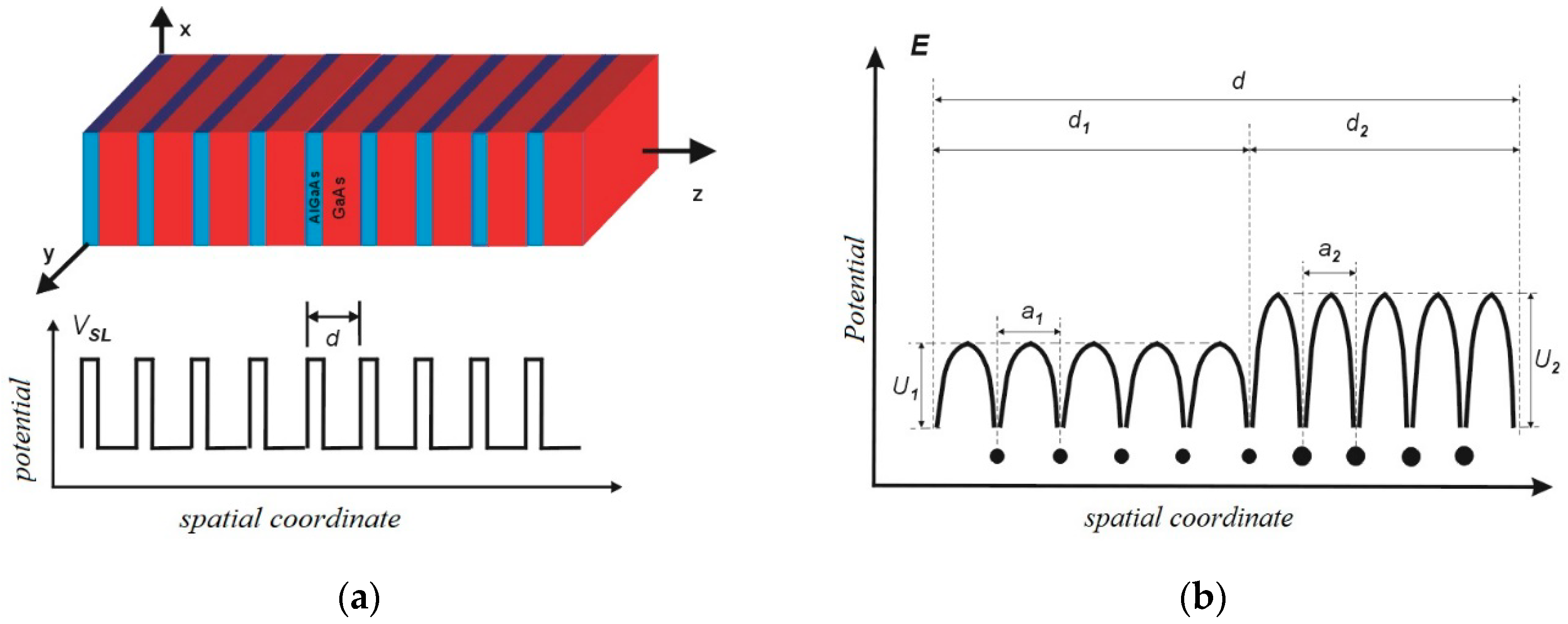
1. Introduction
2. The Methods and Algorithms of Superlattice Simulations
2.1. The Main Algorithm of Calculations
2.2. The Schrödinger Equation
2.3. The Base of Quantum States Construction
2.4. The NEGF Formalism
2.5. Solving the Poisson Equation
2.6. The Results Presentation
3. Conclusions
Funding
Acknowledgments
Conflicts of Interest
References
- Kazarinov, R.F.; Suris, R.A. Electric and electromagnetic properties of semiconductors with a superlattice. Sov. Phys. Semicond. 1972, 6, 120. [Google Scholar]
- Columbo, L.L.; Barbieri, S.; Sirtori, C.; Brambilla, M. Dynamics of a broad-band quantum cascade laser: From chaos to coherent dynamics and mode-locking. Opt. Express 2018, 26, 2829–2847. [Google Scholar] [CrossRef] [PubMed]
- Pierściński, K.; Kuźmicz, A.; Pierścińska, D.; Sobczak, G.; Sakowicz, M.; Gutowski, P.; Janus, K.; Chmielewski, K.; Bugajski, M. Optimization of cavity designs of tapered AlInAs/InGaAs/InP quantum cascade lasers emitting at 4.5 µm. Ieee J. Sel. Top. Quantum Electron. 2019, 25, 99. [Google Scholar]
- Franckie, M.; Faist, J. Bayesian Optimization of Terahertz Quantum Cascade Lasers. Phys. Rev. Appl. 2020, 13, 034025. [Google Scholar] [CrossRef]
- Tsu, R.; Esaki, L. Tunneling in a finite superlattice. Appl. Phys. Lett. 1973, 22, 562. [Google Scholar]
- Mukherji, D.; Nag, B.R. Miniband parameters of semiconductor superlattices. Solid -State Electron. 1975, 18, 1107–1109. [Google Scholar] [CrossRef]
- Saha, S.; Kumar, J. Complete rate equation modelling of quantum cascade lasers for the analysis of temperature effects. Infrared Phys. Technol. 2016, 79, 85–90. [Google Scholar] [CrossRef]
- Pereira, M.F.; Zubelli, J.P.; Winge, D.; Wacker, A.; Rodrigues, A.S.; Anfertev, V.; Vaks, V. Theory and measurements of harmonic generation in semiconductor superlattices with applications in the 100 GHz to 1 THz range. Phys. Rev. B 2017, 96, 045306. [Google Scholar] [CrossRef]
- Borowik, P.; Thobel, J.-L.; Adamowicz, L. Monte Carlo modeling applied to studies of quantum cascade lasers. Opt. Quantum Electron. 2017, 49, 96. [Google Scholar] [CrossRef]
- Jirauschek, C.; Okeil, H.; Lugli, P. Monte Carlo analysis of the terahertz difference frequency generation susceptibility in quantum cascade laser structures. Opt. Express 2015, 23, 1670–1678. [Google Scholar] [CrossRef]
- Datta, S. Electronic Transport in Mesoscopic Systems; Cambridge University Press: Cambridge, UK, 1995. [Google Scholar]
- Keldysh, L.V. Diagram technique for non-equilibrium processes. Sov. Phys. Jetp 1965, 20, 1018–1026. [Google Scholar]
- Hałdaś, G. Implementation of non-uniform mesh in non-equilibrium Green’s function simulations of quantum cascade lasers. J. Comput. Electron. 2019, 18, 1400–1406. [Google Scholar] [CrossRef]
- Hałdaś, G.; Kolek, A.; Pierścińska, D.; Bugajski, M. Tuning quantum cascade laser wavelength by the injector doping. Appl. Phys. B 2018, 124, 144. [Google Scholar] [CrossRef]
- Kolek, A.; Hałdaś, G.; Bugajski, M. Comparison of quantum cascade structures for detection of nitric oxide at ~5.2 μm. Opt. Quantum Electron. 2019, 51, 327. [Google Scholar] [CrossRef]
- Lee, S.-C.; Wacker, A. Nonequilibrium Green’s function theory for transport and gain properties of quantum cascade structures. Phys. Rev. B 2002, 66, 245314. [Google Scholar] [CrossRef]
- Wacker, A. Semiconductor superlattices: A model system for nonlinear transport. Phys. Rep. 2002, 357, 1–111. [Google Scholar] [CrossRef]
- Lee, S.-C.; Banit, F.; Woerner, M.; Wacker, A. Quantum-mechanical wavepacket transport in quantum cascade laser structures. Phys. Rev. B 2006, 73, 245320-1–245320-6. [Google Scholar] [CrossRef]
- Franckie, M.; Bosco, L.; Beck, M.; Bonzon, C.; Mavrona, E.; Scalari, G.; Wacker, A.; Faist, J. Two-well quantum cascade laser optimization by non-equilibrium Green’s function modelling. Appl. Phys. Lett. 2018, 112, 021104. [Google Scholar] [CrossRef]
- Mączka, M.; Pawłowski, S.; Plewako, J. Comparative analysis of selected models of semiconductor superlattices. Electr. Rev. 2011, 8, 93. [Google Scholar]
- Mączka, M.; Pawłowski, S. Wannier function applied to quantum cascade lasers modeling. Przegląd Elektrotechniczny 2013, 12, 245. [Google Scholar]
- Mączka, M.; Hałdaś, G.; Pawłowski, S. Study of quantum states maximal localization in nonsymmetrical semiconductor superlattice structures. In Proceedings of the 2016 13th Selected Issues of Electrical Engineering and Electronics (WZEE), Rzeszow, Poland, 4–8 May 2016; pp. 1–5. [Google Scholar]
- Mączka, M.; Hałdaś, G. Calculations of transport parameters in semiconductor superlattices based on the Green’s functions method in different Hamiltonian representations. Bull. Pol. Acad. Sci. Tech. Sci. 2019, 67, 3. [Google Scholar]
- Callebaut, H.; Hu, Q. Importance of coherence for electron transport in terahertz quantum cascade lasers. J. Appl. Phys. 2005, 98, 104505. [Google Scholar] [CrossRef]
- Büttiker, M. Four-Terminal Phase-Coherent Conductance. Phys. Rev. Lett. 1986, 57, 1761–1764. [Google Scholar] [CrossRef]
- Venugopal, R.; Paulsson, M.; Goasguen, S.; Datta, S.; Lundstrom, M. A simple quantum mechanical treatment of scattering in nanoscale transistors. J. Appl. Phys. 2003, 93, 5613–5625. [Google Scholar] [CrossRef]
- Wacker, A. Coherence and spatial resolution of transport in quantum cascade lasers. Phys. Status Solidi 2008, 5, 215–220. [Google Scholar] [CrossRef]
- Press, W.H.; Flannery, B.P.; Teukolsky, S.A.; Vetterling, W.T. Newton-Raphson method using derivatives and Newton-Raphson methods for nonlinear systems of equations, §9.4 and 9.6 in Numerical Recipes in FORTRAN. In The Art of Scientific Computing, 2nd ed.; Cambridge University Press: Cambridge, UK, 1992. [Google Scholar]


| Number of Structure | Materials of Heterostructures | The Dimensions of the Structures (Barriers Are Denoted in Bold) (nm) | ΔEc (eV) |
|---|---|---|---|
| 1. | AlGaAs/GaAs | 6.5, 2.5 | 0.22 |
| 2. | 7.8, 2.4, 6.4, 3.8, 14.8, 2.4, 9.4, 5.4 | 0.15 | |
| 3. | 4.6, 1.9, 1.1, 5.4, 1.1, 4.8, 2.8, 3.4, 1.7, 3.0, 1.8, 2.8, 2.0, 3.0, 2.6, 3.0 | 0.39 |
| No. of State | 0 mV /Period | 10 mV /Period | 20 mV /Period | 30 mV /Period | 40 mV /Period | 50 mV /Period |
|---|---|---|---|---|---|---|
| µzB (meV) | µzB (meV) | µzB (meV) | µzB (meV) | µzB (meV) | µzB (meV) | |
| 5’ | 62.25 | 72.33 | 82.66 | 93.51 | 105.41 | 118.31 |
| 4’ | 50.9 | 63.76 | 76.53 | 88.97 | 100.64 | 90.81 |
| 3’ | 33.92 | 48.1 | 62.17 | 76.09 | 89.76 | 88.03 |
| 2’ | 29.12 | 36.48 | 44.02 | 51.68 | 49.72 | 68.09 |
| 1’ | 14.67 | 24.42 | 34.03 | 46.05 | 52.42 | 60.89 |
| 5 | 62.25 | 62.33 | 62.65 | 63.51 | 65.4 | 78.31 |
| 4 | 50.9 | 53.76 | 56.53 | 58.96 | 60.53 | 40.81 |
| 3 | 33.92 | 38.11 | 42.13 | 43.41 | 59.78 | 38.03 |
| 2 | 29.12 | 26.48 | 24.01 | 21.67 | 20.52 | 18.08 |
| 1 | 14.67 | 14.42 | 14.03 | 16.05 | 12.42 | 10.89 |
| 5” | 62.25 | 52.33 | 42.65 | 33.5 | 25.4 | 28.31 |
| 4” | 50.9 | 43.75 | 36.52 | 28.95 | 19.78 | −9.19 |
| 3” | 33.92 | 28.11 | 22.12 | 13.41 | 19.72 | −11.9 |
| 2” | 29.12 | 16.49 | 3.96 | −8.37 | −20.36 | −31.86 |
| 1” | 14.67 | 4.42 | −5.97 | −16.59 | −27.59 | −39.11 |
Publisher’s Note: MDPI stays neutral with regard to jurisdictional claims in published maps and institutional affiliations. |
© 2020 by the author. Licensee MDPI, Basel, Switzerland. This article is an open access article distributed under the terms and conditions of the Creative Commons Attribution (CC BY) license (http://creativecommons.org/licenses/by/4.0/).
Share and Cite
Mączka, M. Effective Simulations of Electronic Transport in 2D Structures Based on Semiconductor Superlattice Infinite Model. Electronics 2020, 9, 1845. https://doi.org/10.3390/electronics9111845
Mączka M. Effective Simulations of Electronic Transport in 2D Structures Based on Semiconductor Superlattice Infinite Model. Electronics. 2020; 9(11):1845. https://doi.org/10.3390/electronics9111845
Chicago/Turabian StyleMączka, Mariusz. 2020. "Effective Simulations of Electronic Transport in 2D Structures Based on Semiconductor Superlattice Infinite Model" Electronics 9, no. 11: 1845. https://doi.org/10.3390/electronics9111845
APA StyleMączka, M. (2020). Effective Simulations of Electronic Transport in 2D Structures Based on Semiconductor Superlattice Infinite Model. Electronics, 9(11), 1845. https://doi.org/10.3390/electronics9111845