Modified Topology for Three-Phase Multilevel Inverters Based on a Developed H-Bridge Inverter

Abstract
:1. Introduction
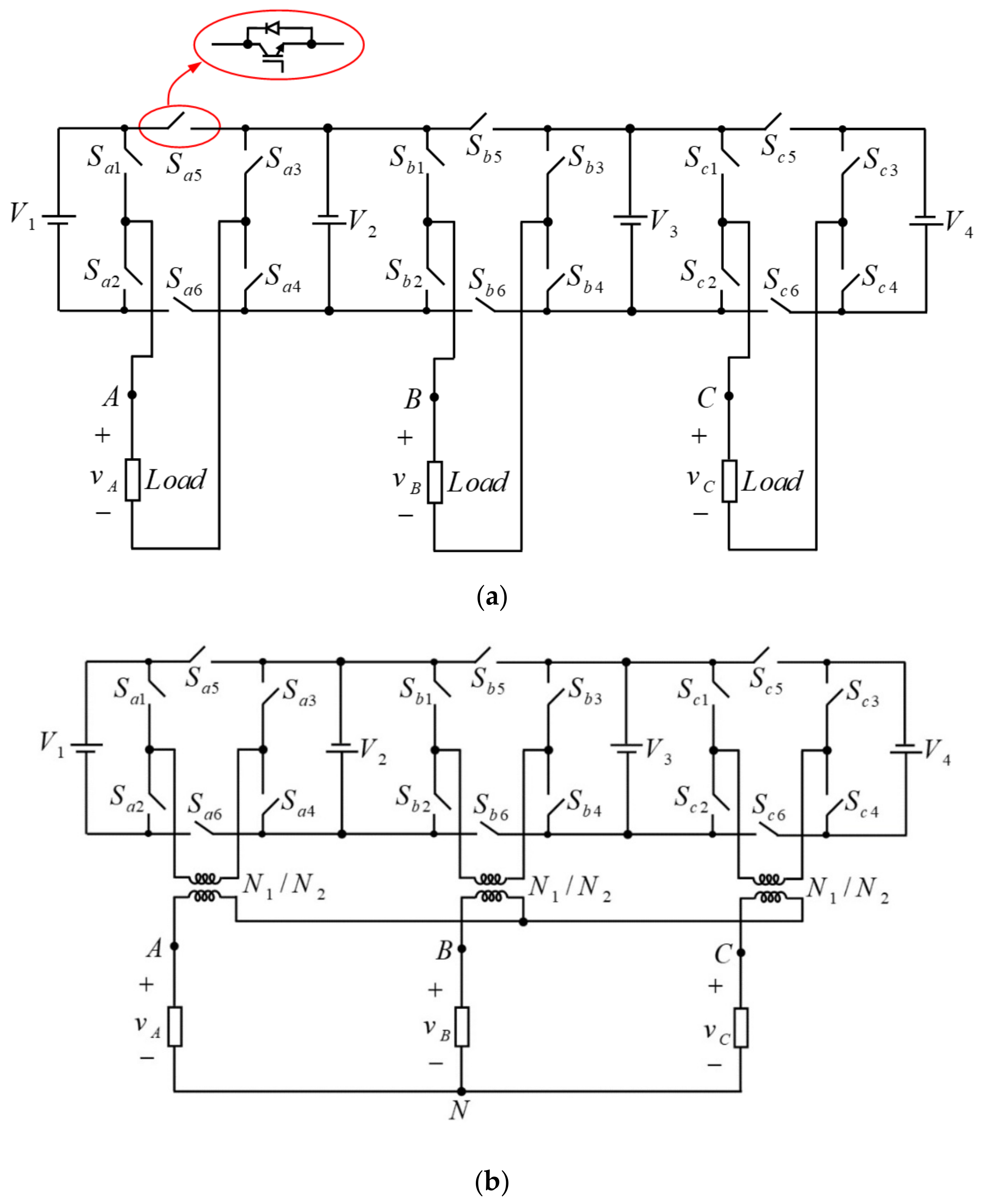
2. Proposed Topology
2.1. Inverter Losses
2.1.1. Switching Losses
2.1.2. Conduction Losses
3. Comparison with Other 7-Levels Inverters
4. Simulation and Experimental Results
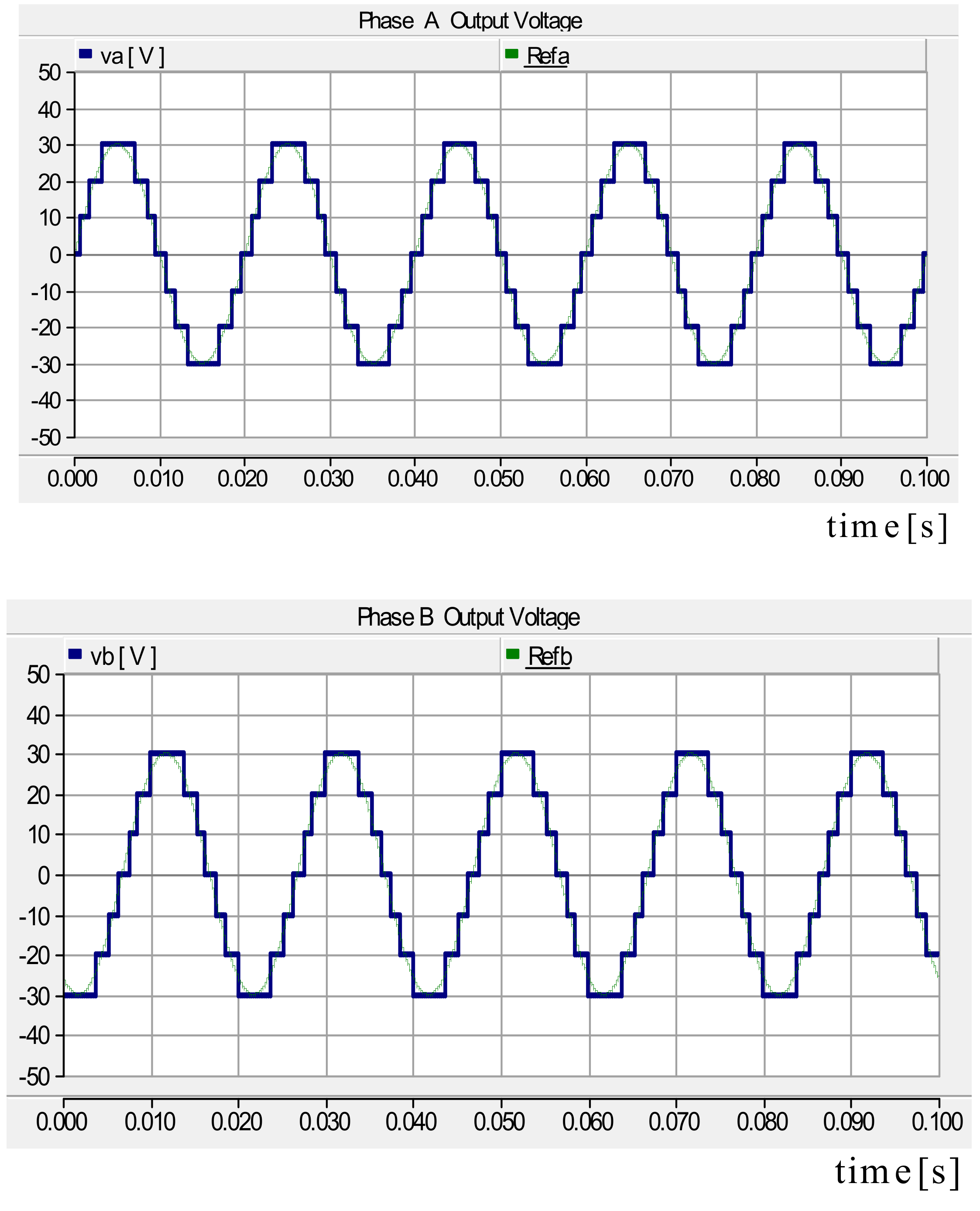
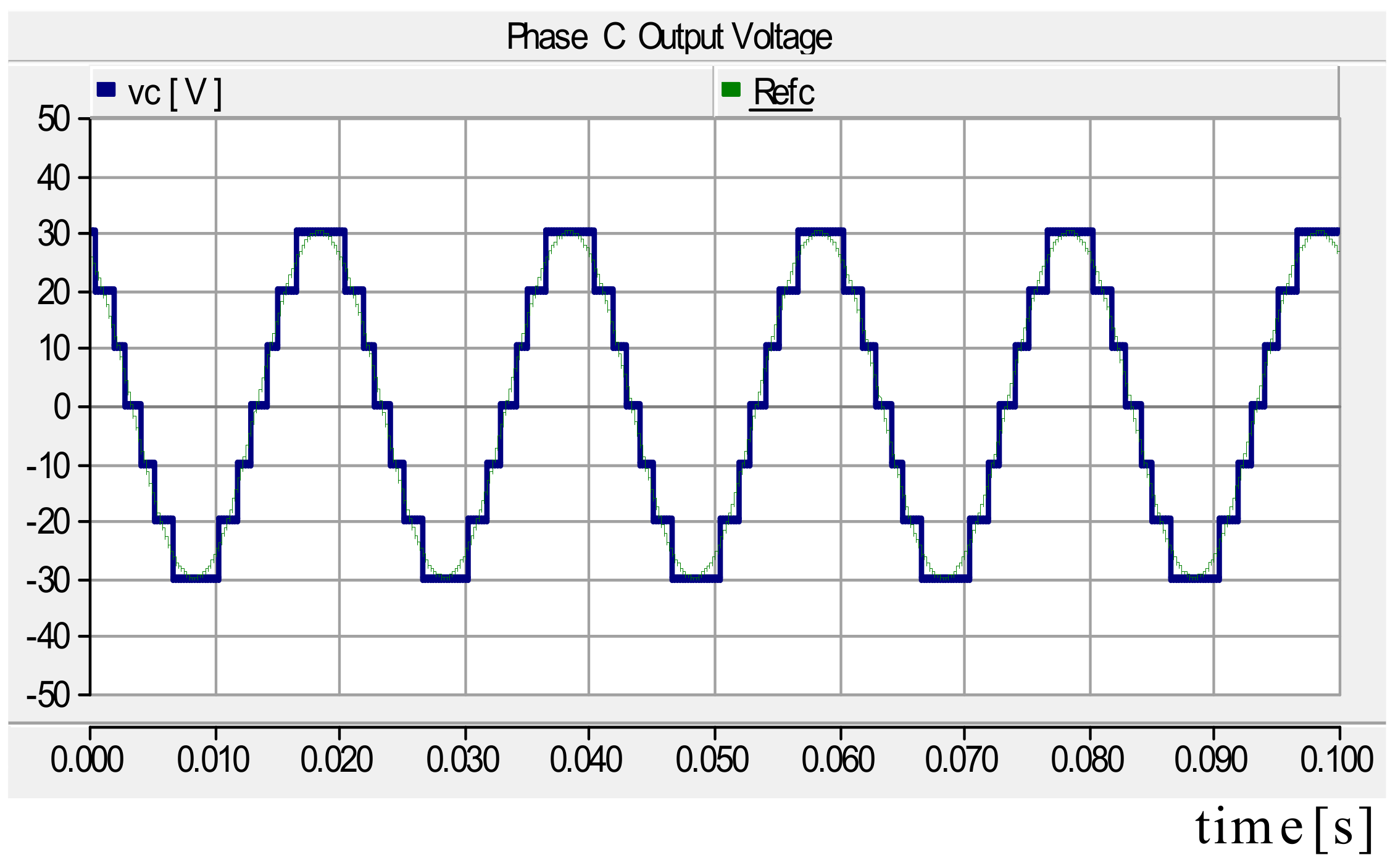
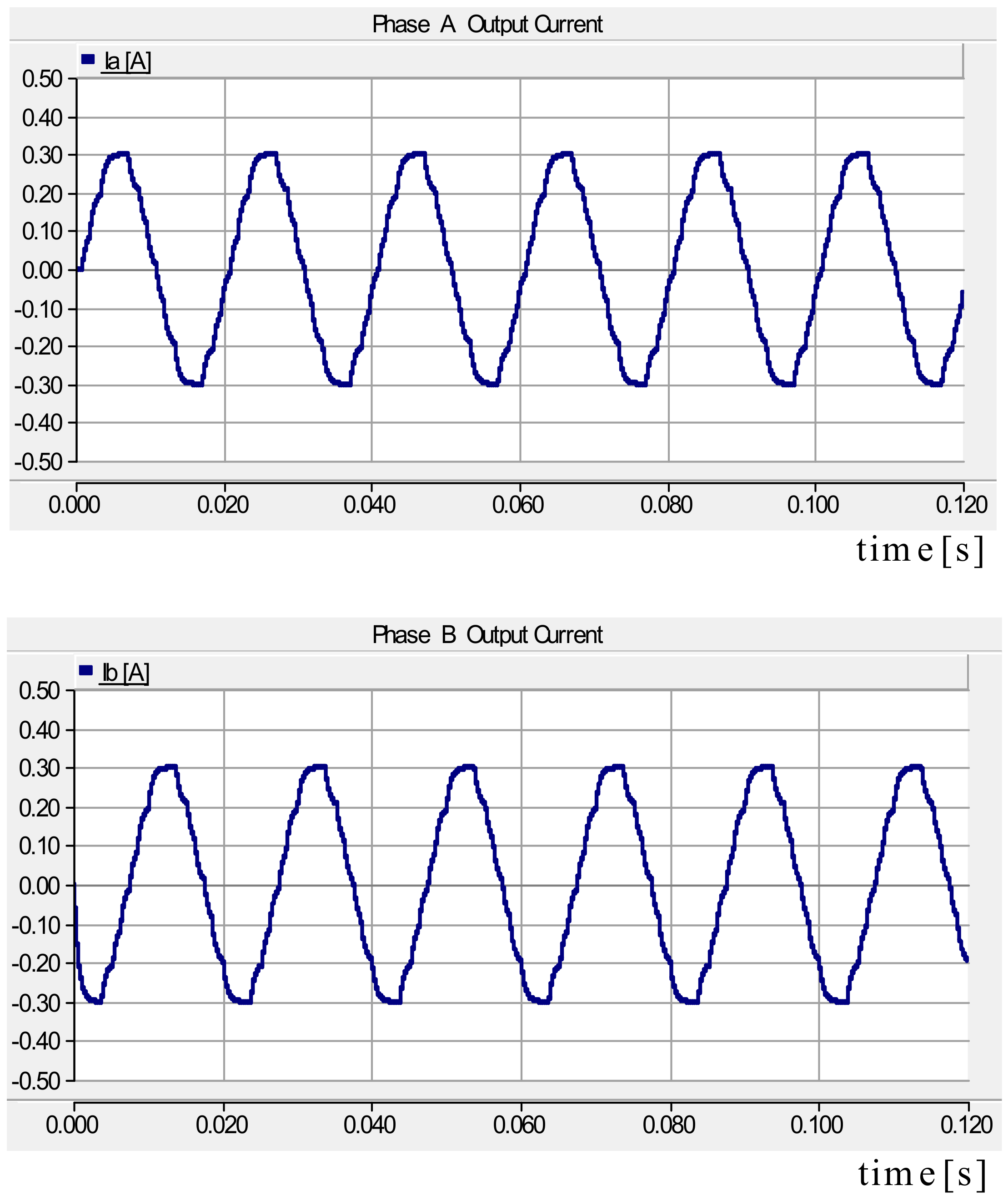
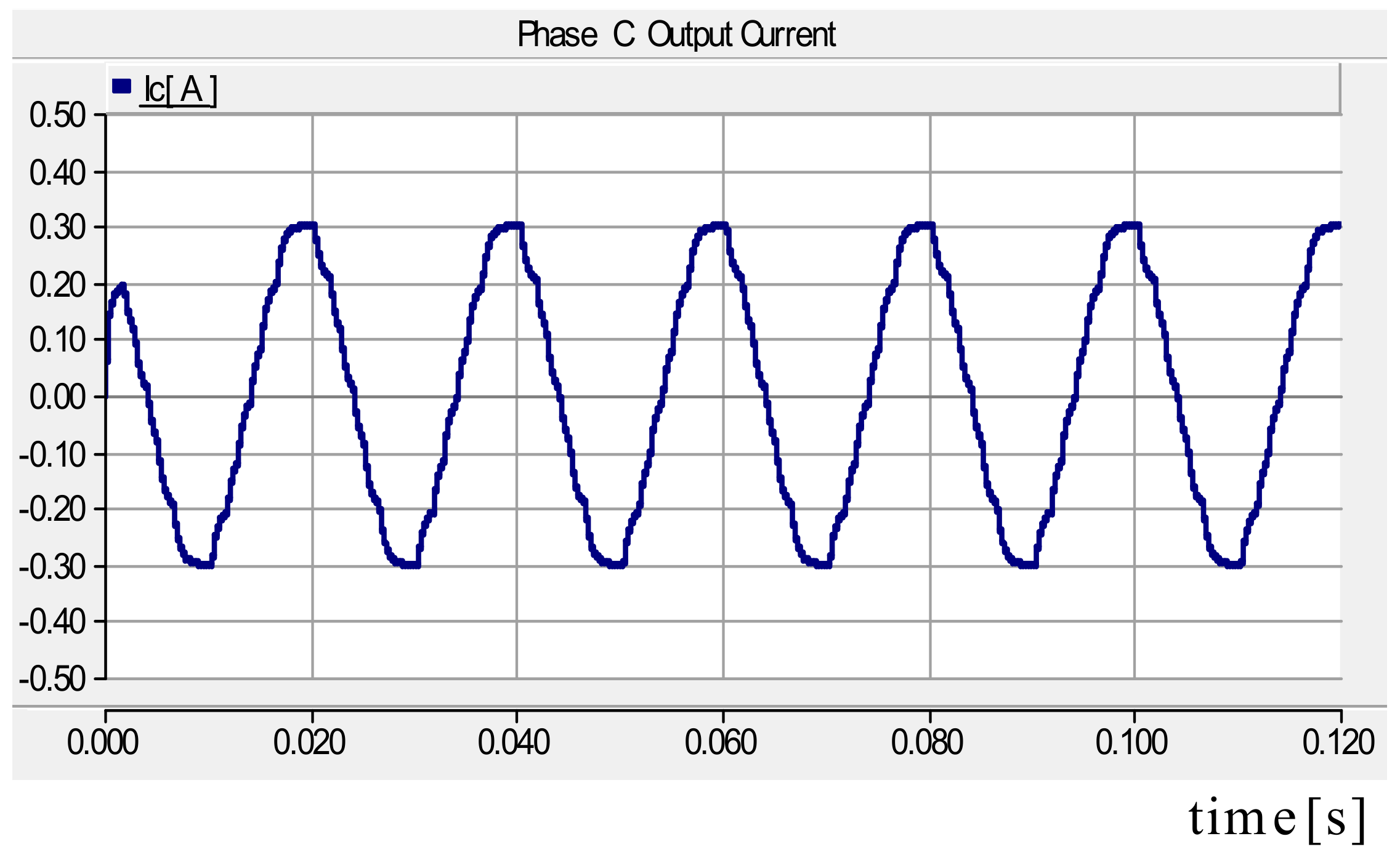
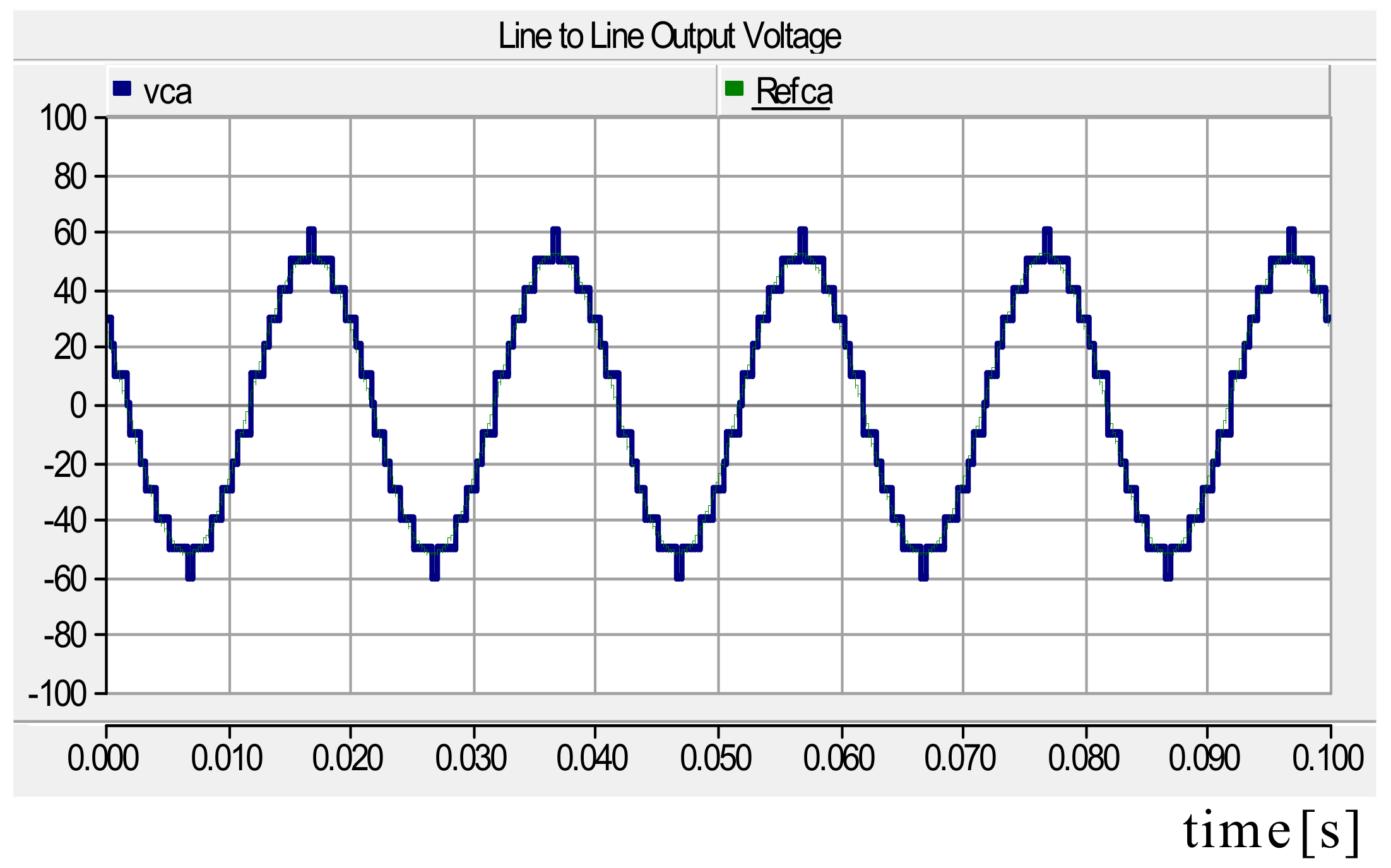
4.1. Simulation Results
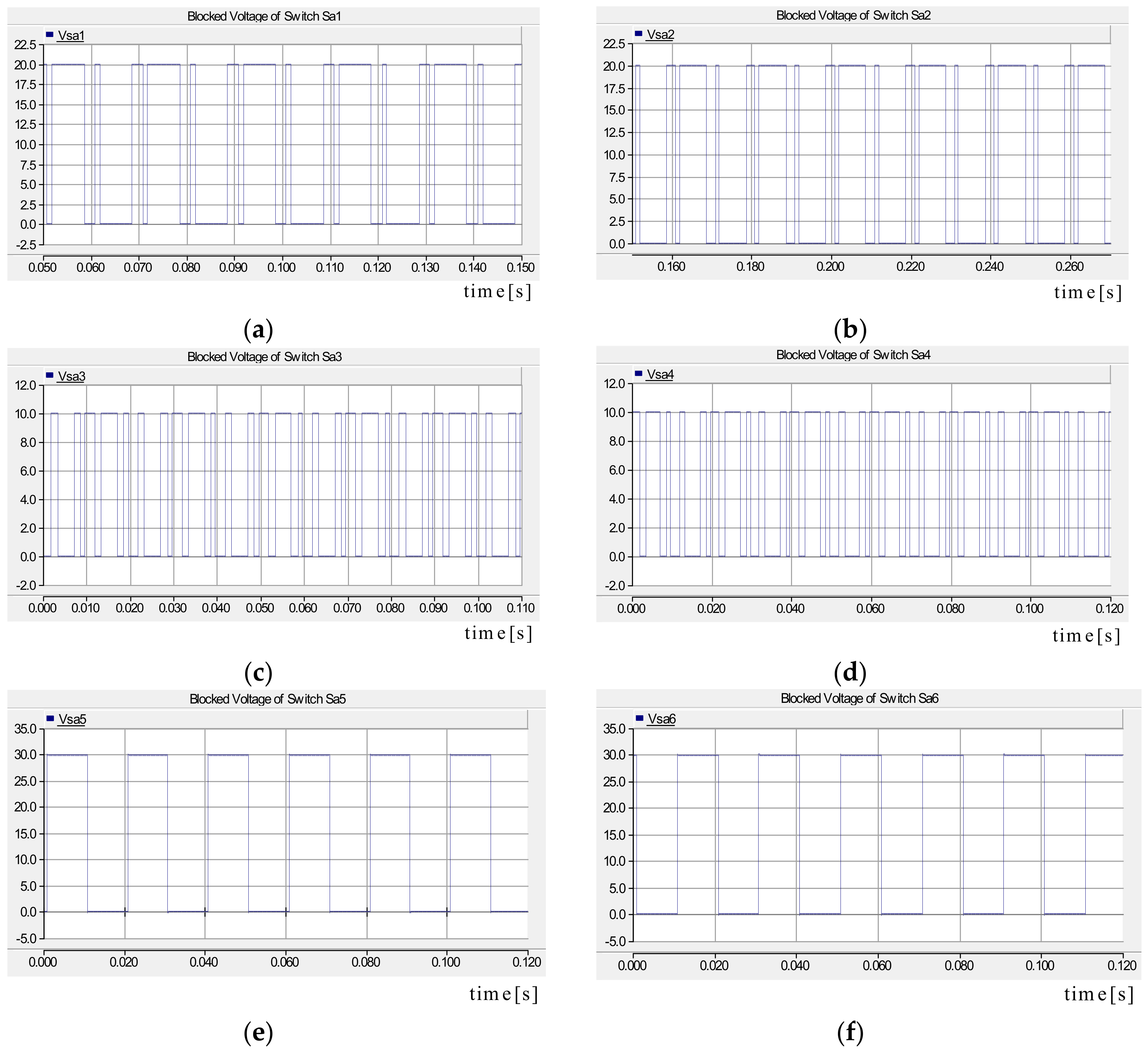
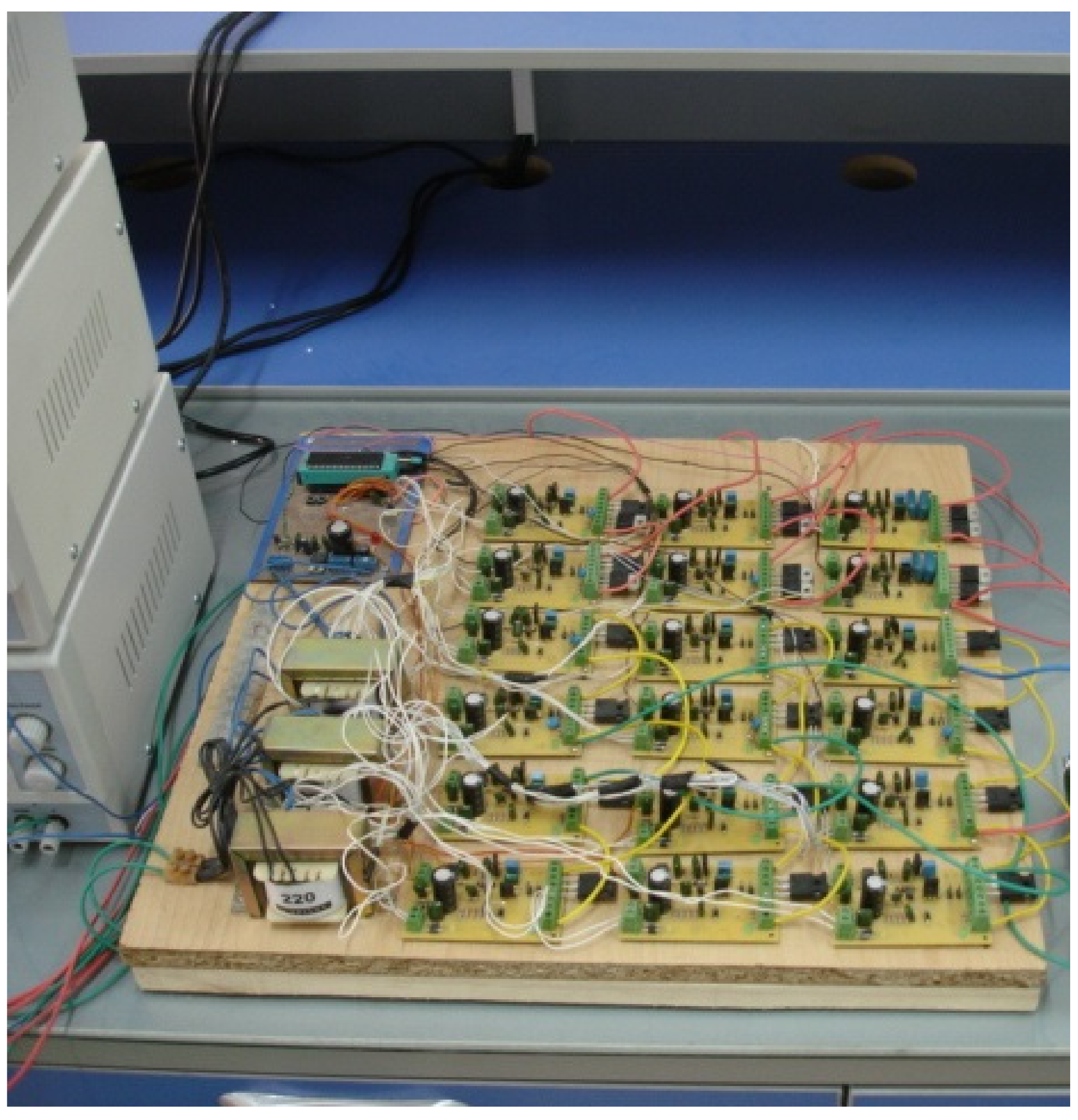
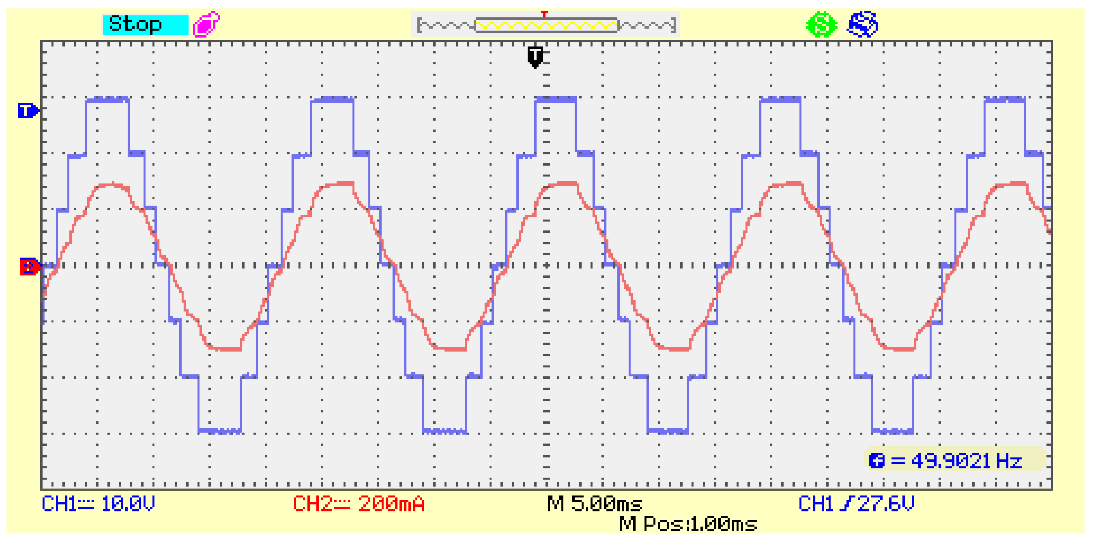
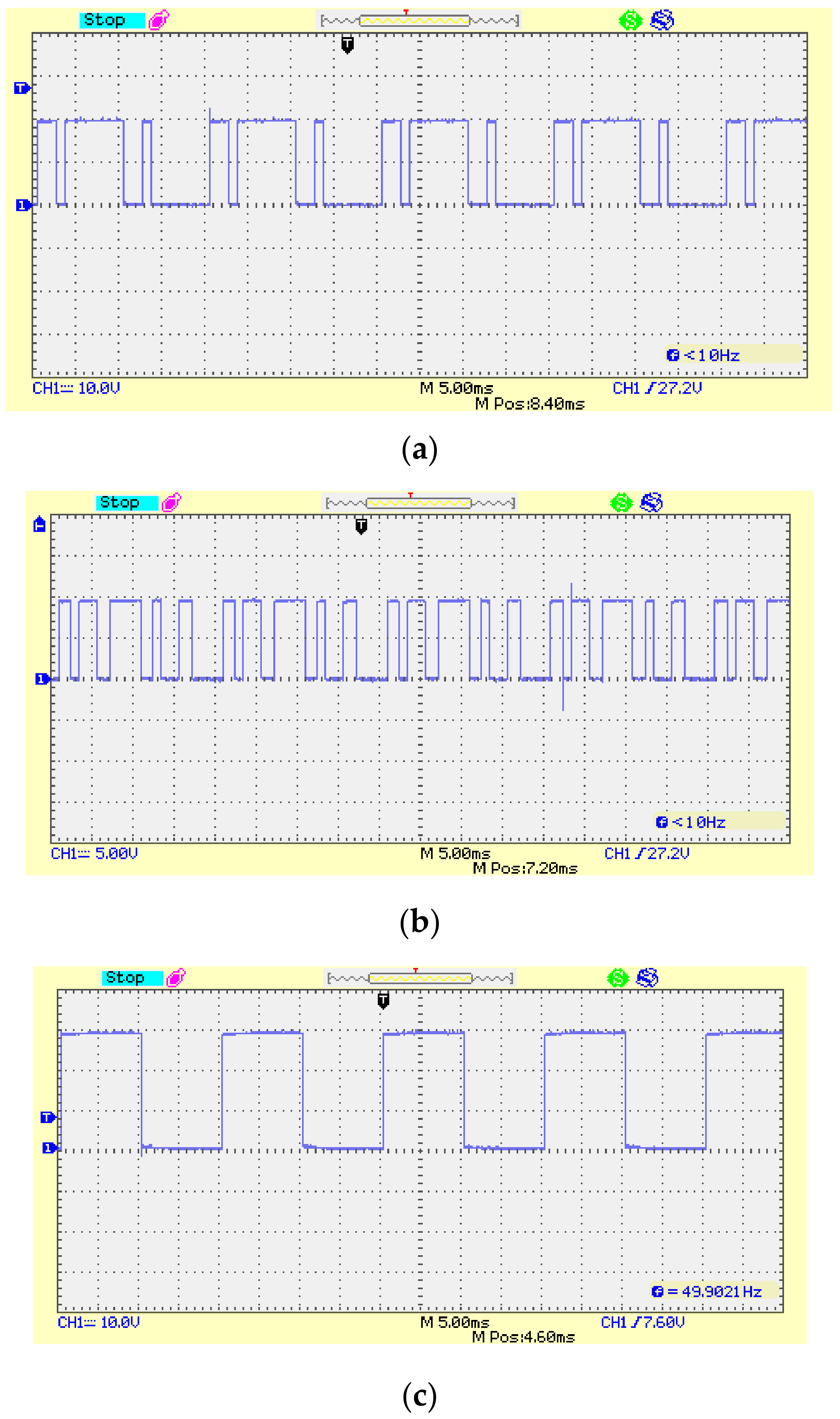
4.2. Experimental Results
5. Conclusions
Author Contributions
Funding
Conflicts of Interest
References
- Masoudinia, F.; Babaei, E.; Sabahi, M.; Alipour, H. New Basic Unit and Cascaded Multilevel Inverters with Reduced Power Electronic Devices. Int. J. Electron. 2020, 107, 1177–1194. [Google Scholar] [CrossRef]
- McGrath, B.P.; Holmes, D.G. Natural capacitor voltage balancing for a flying capacitor converter induction motor drive. IEEE Trans. Power Electron. 2009, 24, 1554–1561. [Google Scholar] [CrossRef]
- Babaei, E. A Cascade multilevel converter topology with reduced number of switches. IEEE Trans. Power Electron. 2008, 23, 2657–2664. [Google Scholar] [CrossRef]
- Kim, J.-H.; Sul, S.-K.; Enjeti, P.N. A carrier-based PWM method with optimal switching sequence for a multilevel four-leg voltage-source inverter. IEEE Trans. Ind. Appl. 2008, 44, 1239–1248. [Google Scholar] [CrossRef]
- Buccella, C.; Cecati, C.; Cimoroni, M.G.; Razi, K. Analytical method for pattern generation in five-level cascaded h-bridge inverter using selective harmonic elimination. IEEE Trans. Ind. Electron. 2014, 61, 5811–5819. [Google Scholar] [CrossRef]
- Leon, J.I.; Kouro, S.; Vazquez, S.; Portillo, R.; Franquelo, L.G.; Carrasco, J.M.; Rodriguez, J. Multidimensional modulation technique for cascaded multilevel converters. IEEE Trans. Ind. Electron. 2010, 58, 412–420. [Google Scholar] [CrossRef] [Green Version]
- Lesnicar, A.; Marquardt, R. An innovative modular multilevel converter topology suitable for a wide power range. In Proceedings of the 2003 IEEE Bologna Power Tech Conference Proceedings, Bologna, Italy, 23–26 June 2003. [Google Scholar] [CrossRef]
- Babaei, E.; Kangarlu, M.F.; Sabahi, M.; Pahlavani, M.R.A. Cascaded multilevel inverter using sub-multilevel cells. Electr. Power Syst. Res. 2013, 96, 101–110. [Google Scholar] [CrossRef]
- Malinowski, M.; Gopakumar, K.; Rodriguez, J.; Perez, M.A. A survey on cascaded multilevel inverters. IEEE Trans. Ind. Electron. 2009, 57, 2197–2206. [Google Scholar] [CrossRef]
- Ebrahimi, J.; Babaei, E.; Gharehpetian, G.B. A new topology of cascaded multilevel converters with reduced number of components for high-voltage applications. IEEE Trans. Power Electron. 2011, 26, 3109–3118. [Google Scholar] [CrossRef]
- Tian, H.; Li, Y.; Li, Y.W. A Novel Seven-Level Hybrid-Clamped (HC) Topology for Medium-Voltage Motor Drives. IEEE Trans. Power Electron. 2017, 33, 5543–5547. [Google Scholar] [CrossRef]
- Yadav, A.K.; Gopakumar, K.; Umanand, L.; Bhattacharya, S.; Jarzyna, W. A Hybrid 7-Level Inverter Using Low-Voltage Devices and Operation with Single DC-Link. IEEE Trans. Power Electron. 2019, 34, 9844–9853. [Google Scholar] [CrossRef]
- Sheng, W.; Ge, Q.; Weihui, S. A Novel Seven-Level ANPC Converter Topology and Its Commutating Strategies. IEEE Trans. Power Electron. 2017, 33, 7496–7509. [Google Scholar] [CrossRef]
- Hasan, M.; Abu-Siada, A.; Dahidah, M.S.A. A three-phase symmetrical DC-Link multilevel inverter with reduced number of DC sources. IEEE Trans. Power Electron. 2017, 33, 8331–8340. [Google Scholar] [CrossRef]
- Sabyasachi, S.; Borghate, V.B.; Karasani, R.R.; Maddugari, S.K.; Suryawanshi, H.M. A Fundamental Frequency Hybrid Control Technique Based Three Phase Cascaded Multilevel Inverter Topology. IEEE Access 2017, 5, 26912–26921. [Google Scholar]
- Yu, H.; Chen, B.; Yao, W.; Lu, Z. Hybrid Seven-Level Converter Based on T-Type Converter and H-Bridge Cascaded Under SPWM and SVM. IEEE Trans. Power Electron. 2017, 33, 689–702. [Google Scholar] [CrossRef]
- Sun, X.; Wang, B.; Zhou, Y.; Wang, W.; Du, H.; Lu, Z. A Single DC Source Cascaded Seven-Level Inverter Integrating Switched-Capacitor Techniques. IEEE Trans. Ind. Electron. 2016, 63, 7184–7194. [Google Scholar] [CrossRef]
- Sanjeevan, A.R.; Kaarthik, R.S.; Gopakumar, K.; Rajeevan, P.; Leon, J.I.; Franquelo, L.G. Reduced common-mode voltage operation of a new seven-level hybrid multilevel inverter topology with a single DC voltage source. IET Power Electron. 2016, 9, 519–528. [Google Scholar] [CrossRef]
- Saeidabadi, S.; Gandomi, A.A.; Hosseini, S.H.; Sabahi, M.; Gandomi, Y.A. New improved three-phase hybrid multilevel inverter with reduced number of components. IET Power Electron. 2017, 10, 1403–1412. [Google Scholar] [CrossRef]
- Karasani, R.R.; Borghate, V.B.; Meshram, P.M.; Suryawanshi, H.M.; Sabyasachi, S. A three-phase hybrid cascaded modular multilevel inverter for renewable energy environment. IEEE Trans. Power Electron. 2016, 32, 1070–1087. [Google Scholar]
- Siwakoti, Y.P.; Mahajan, A.; Rogers, D.; Blaabjerg, F. A Novel Seven-Level Active Neutral Point Clamped Converter with Reduced Active Switching Devices and DC-link Voltage. IEEE Trans. Power Electron. 2019, 34, 10492–10508. [Google Scholar]
- Raushan, R.; Mahato, B.; Jana, K.C. Comprehensive analysis of a novel three-phase multilevel inverter with minimum number of switches. IET Power Electron. 2016, 9, 1600–1607. [Google Scholar] [CrossRef]
- Tirupathi, A.; Kirubakaran, A.; Tirumala, S.V. A Seven-Level VSI with a Front-end Cascaded Three-Level Inverter and Flying Capacitor fed H-Bridge. IEEE Trans. Ind. Appl. 2019, 55, 6073–6088. [Google Scholar]
- Babaei, E.; Alilu, S.; Laali, S. A new general topology for cascaded multilevel inverters with reduced number of components based on developed H-bridge. IEEE Trans. Ind. Electron. 2013, 61, 3932–3939. [Google Scholar] [CrossRef]
- Pan, Z.; Peng, F.Z.; Corzine, K.A.; Stefanovic, V.R.; Leuthen, J.M.; Gataric, S. Voltage balancing control of diode clamped multilevel rectifier/inverter systems. IEEE Trans. Ind. Electron. 2005, 41, 1698–1706. [Google Scholar] [CrossRef]
- Gaur, P.; Singh, P. Various control strategies for medium voltage high power multilevel converters: A review. In Proceedings of the 2014 Recent Advances in Engineering and Computational Sciences (RAECS), Chandigarh, India, 6–8 March 2014; pp. 1–6. [Google Scholar]
- Babaei, E.; Laali, S.; Bayat, Z. A Single-phase cascaded multilevel inverter based on a new basic unit with reduced number of power switches. IEEE Trans. Ind. Electron. 2014, 62, 922–929. [Google Scholar] [CrossRef]


| State | Switches | VA | Switches | VB | Switches | VC |
|---|---|---|---|---|---|---|
| I | Sa2, Sa3, Sa6 | Vdc | Sb2, Sb3, Sa5 | Vdc | Sc2, Sc3, Sc6 | Vdc |
| II | Sa1, Sa4, Sa6 | 2Vdc | Sb1, Sb4, Sa5 | 2Vdc | Sc1, Sc4, Sc6 | 2Vdc |
| III | Sa1, Sa3, Sa6 | 3 Vdc | Sb2, Sb4, Sa5 | 3 Vdc | Sc1, Sc3, Sc6 | 3Vdc |
| IV | Sa1, Sa3, Sa5 Sa2, Sa4, Sa6 | 0 | Sb1, Sb3, Sa5 Sb2, Sb4, Sa6 | 0 | Sc1, Sc3, Sc5 Sc2, Sc4, Sc6 | 0 |
| V | Sa1, Sa4, Sa5 | −Vdc | Sb1, Sb4, Sa6 | −Vdc | Sc4, Sc1, Sc5 | −Vdc |
| VI | Sa2, Sa3, Sa5 | −2Vdc | Sb2, Sb3, Sa6 | −2Vdc | Sc2, Sc3, Sc5 | −2Vdc |
| VII | Sa2, Sa4, Sa5 | −3Vdc | Sb1, Sb3, Sa6 | −3Vdc | Sc2, Sc4, Sc5 | −3Vdc |
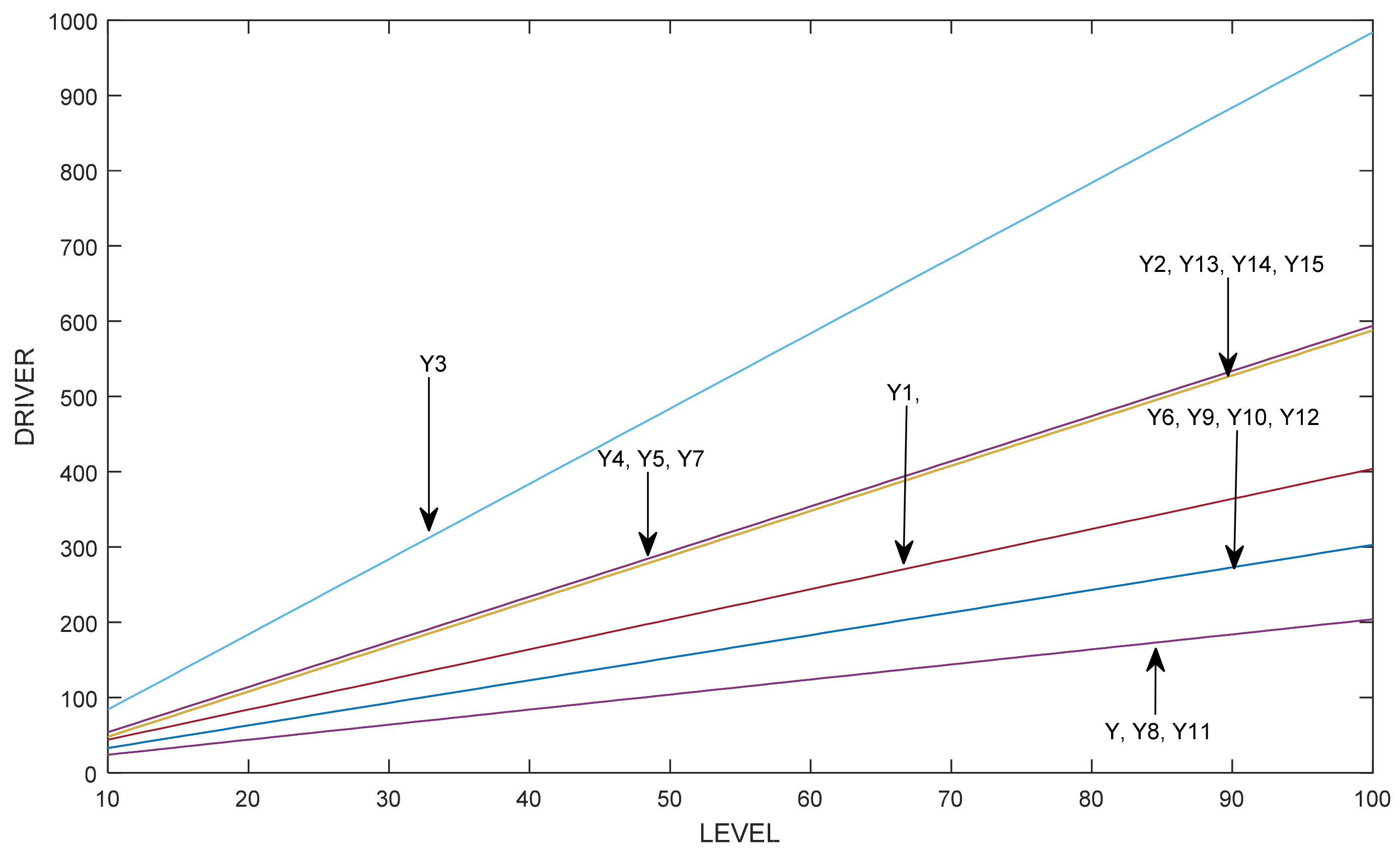
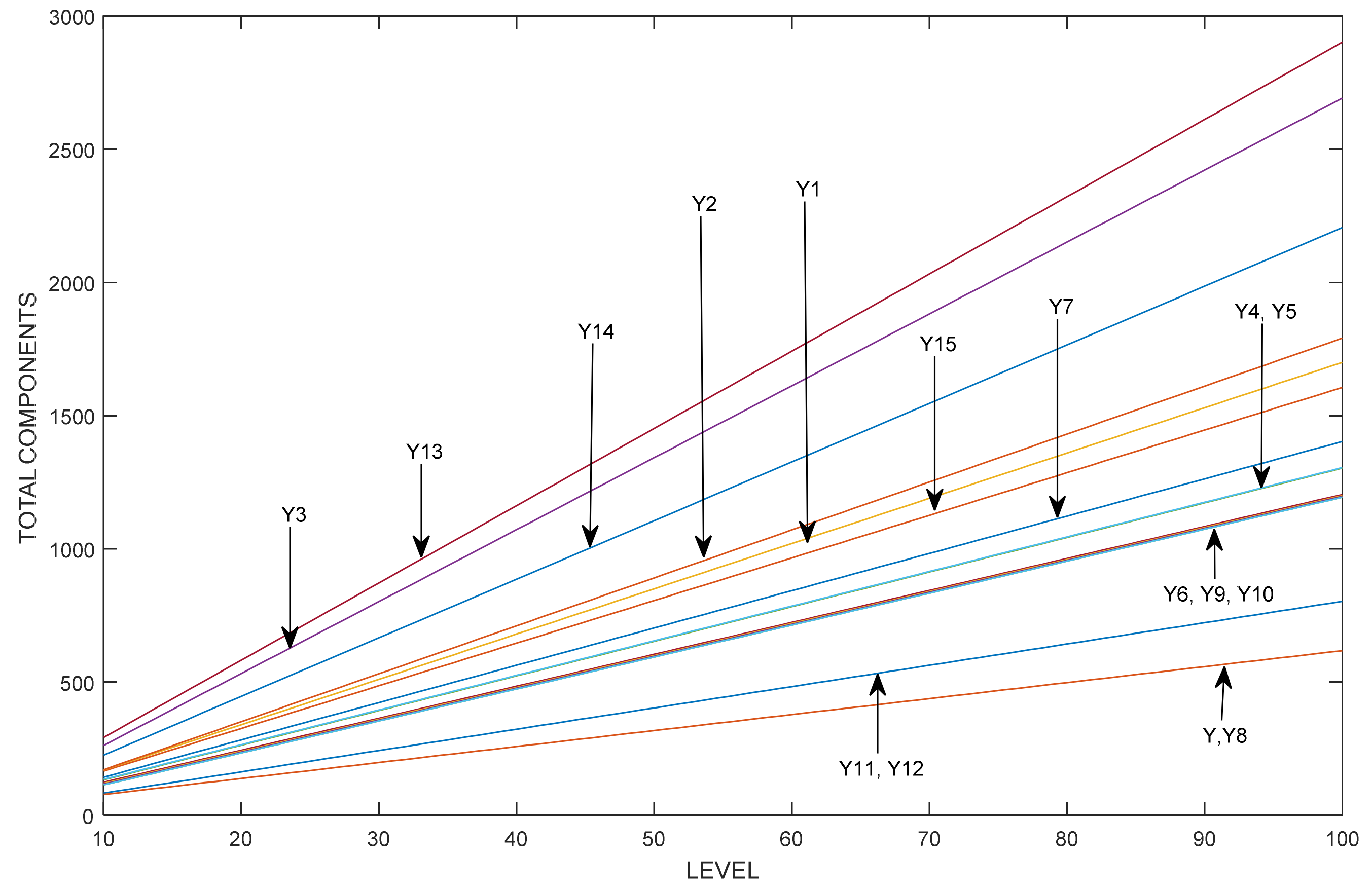
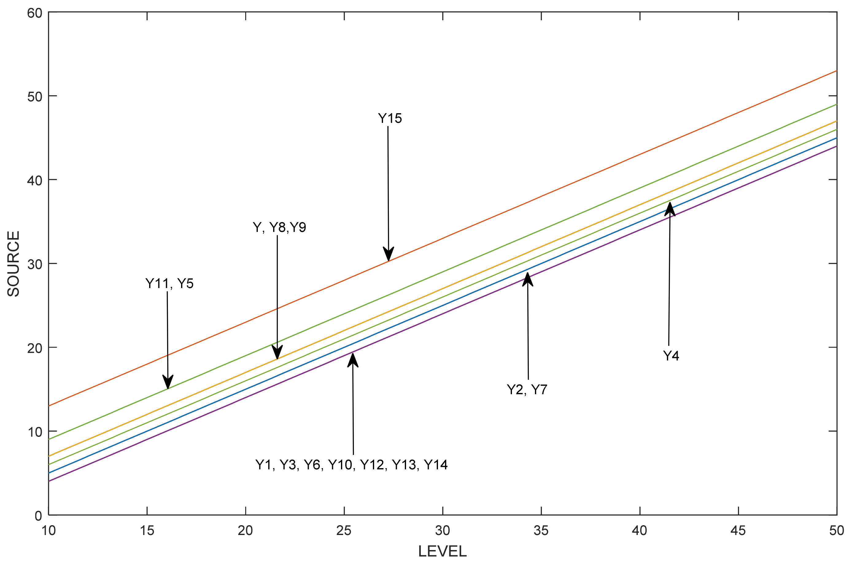
| Topology | Nlevel | NIGBT | NDC | NDriver | NMD | NCD | NCF | NC | NT | NTotal |
|---|---|---|---|---|---|---|---|---|---|---|
| Proposed | 7 | 18 | 4 | 18 | 18 | 0 | 0 | 0 | 1 | 59 |
| [11] | 7 | 36 | 1 | 36 | 36 | 0 | 0 | 6 | 1 | 116 |
| [12] | 7 | 36 | 2 | 36 | 36 | 0 | 0 | 9 | 0 | 119 |
| [13] | 7 | 54 | 1 | 54 | 55 | 0 | 0 | 17 | 0 | 181 |
| [14] | 7 | 30 | 3 | 30 | 30 | 0 | 0 | 0 | 1 | 94 |
| [15] | 7 | 30 | 6 | 30 | 30 | 0 | 0 | 0 | 0 | 96 |
| [16] | 7 | 24 | 1 | 24 | 30 | 0 | 0 | 9 | 0 | 88 |
| [17] | 7 | 14 | 3 | 14 | 12 | 0 | 0 | 3 | 0 | 46 |
| [18] | 7 | 30 | 2 | 30 | 30 | 0 | 0 | 9 | 0 | 101 |
| [19] | 7 | 18 | 6 | 18 | 18 | 0 | 0 | 0 | 0 | 60 |
| [20] | 9 | 24 | 4 | 24 | 24 | 0 | 0 | 8 | 0 | 84 |
| [21] | 7 | 24 | 1 | 24 | 24 | 0 | 0 | 8 | 0 | 81 |
| [22] | 7 | 18 | 6 | 18 | 36 | 0 | 0 | 0 | 0 | 78 |
| [23] | 7 | 24 | 1 | 24 | 24 | 0 | 0 | 5 | 0 | 78 |
| NPC | 7 | 36 | 1 | 36 | 36 | 90 | 0 | 6 | 0 | 205 |
| FC | 7 | 36 | 1 | 36 | 36 | 0 | 45 | 6 | 0 | 160 |
| CHB | 7 | 36 | 9 | 36 | 36 | 0 | 0 | 0 | 0 | 117 |
| Topology | NIGBT | NDriver | NMC | NDC | NTotal |
|---|---|---|---|---|---|
| Y-Proposed | 2(n + 2) | 2(n + 2) | - | n − 3 | (8n + 3) |
| Y1 [11] | 6(n − 1) | 6(n − 1) | n − 7 | n − 6 | (16n + 6) |
| Y2 [12] | 6(n − 1) | 6(n − 1) | n + 3 | n − 5 | 17n |
| Y3 [13] | (10n − 15) − 1 | (10n − 15) − 1 | 2n + 3 | n − 6 | (27n − 8) |
| Y4 [14] | 3(2n − 4) | 3(2n − 4) | - | n − 4 | (13n + 3) |
| Y5 [15] | 3(2n − 4) | 3(2n − 4) | - | n − 1 | (13n + 5) |
| Y6 [16] | 3n + 3 | 3n + 3 | n + 3 | n − 6 | (12n + 4) |
| Y7 [18] | 3(2n − 4) | 3(2n − 4) | n + 3 | n − 5 | (14n + 3) |
| Y8 [19] | 2(n + 2) | 2(n + 2) | - | n − 3 | 3(2n + 4) + 6 |
| Y9 [20] | 3n + 3 | 3n + 3 | n + 1 | n − 3 | 12n |
| Y10 [21] | 3n + 3 | 3n + 3 | n + 1 | n − 6 | 3(4n − 1) |
| Y11 [22] | 2(n + 2) | 2(n + 2) | - | n − 1 | 3(4n − 2) |
| Y12 [23] | 3n + 3 | 3n + 3 | n − 2 | n − 5 | 3(4n −6) |
| Y13 [NPC] | 6(n − 1) | 6(n − 1) | n − 1 | n − 5 | 6(5n + 1) − (n + 4) |
| Y14 [CHB] | 6(n − 1) | 6(n − 1) | n − 1 | n − 5 | (22n + 6) |
| Y15 [FC] | 6(n − 1) | 6(n − 1) | - | n + 3 | 3(6n − 2) − 3 |
| Parameter | Value |
|---|---|
| Input voltage Vdc | V1 = V3 = 20 V, V2 = V4 = 10 V |
| Output Resistance R | 100 Ω |
| Output Inductance L | 55 mH |
| Switching Frequency fs | 4 kHz |
| Output Frequency fo | 50 Hz |
| Modulation Index | 1 |
Publisher’s Note: MDPI stays neutral with regard to jurisdictional claims in published maps and institutional affiliations. |
© 2020 by the authors. Licensee MDPI, Basel, Switzerland. This article is an open access article distributed under the terms and conditions of the Creative Commons Attribution (CC BY) license (http://creativecommons.org/licenses/by/4.0/).
Share and Cite
Tackie, S.N.; Babaei, E. Modified Topology for Three-Phase Multilevel Inverters Based on a Developed H-Bridge Inverter. Electronics 2020, 9, 1848. https://doi.org/10.3390/electronics9111848
Tackie SN, Babaei E. Modified Topology for Three-Phase Multilevel Inverters Based on a Developed H-Bridge Inverter. Electronics. 2020; 9(11):1848. https://doi.org/10.3390/electronics9111848
Chicago/Turabian StyleTackie, Samuel Nii, and Ebrahim Babaei. 2020. "Modified Topology for Three-Phase Multilevel Inverters Based on a Developed H-Bridge Inverter" Electronics 9, no. 11: 1848. https://doi.org/10.3390/electronics9111848