Abstract
This paper presents a switched capacitive reference driver (SCRD) with a low-energy switching scheme. In order to reduce the performance degradation resulting from a signal-dependent voltage drop in a capacitive reference driver (CRD) without increasing the capacitance (CREF) of a CRD, the proposed SCRD utilizes the CRD for LSB conversion cycles. In MSB conversion cycles, a supply voltage is used as a reference voltage to save on area and power consumption. As such, the proposed SCRD significantly relaxes the required CREF, and does not necessitate bit weight calibration or compensation requiring an auxiliary capacitor-based digital-to-analog converter (CDAC). To evaluate the proposed SCRD, a prototype 12-bit 40-MS/s SAR ADC is fabricated in a 65 nm CMOS process. With near Nyquist frequency, the measured spurious-free dynamic range (SFDR) of the SAR ADC with the SCRD is 80.6 dB, which is about a 16 dB improvement from the SFDR of a SAR ADC with a CRD only.
1. Introduction
Successive approximation register (SAR) analog-to-digital converters (ADCs) are the fastest-growing structure due to the advantage of speed improvement from technology scaling. Besides, their excellent energy efficiency is suitable for overall frequency bands, from biomedical and internet of things (IoT) nodes [1,2], to next-generation wireless and network high-speed links [3,4].
In the SAR ADC, a typical way to offer a reference voltage is an active reference driver, as shown in Figure 1a. The active reference driver not only provides a stable reference voltage against on-chip supply noise, but also prevents slow settling from bondwire inductance. However, the active reference driver is power-hungry and is responsible for nearly half of the power consumption of the ADC [5,6]. Furthermore, it may require a higher supply voltage than that of a core ADC, because the reference voltage is often the same as the supply voltage of the core ADC in many SAR ADCs. Other ways to replace the active reference driver are to use the supply voltage of the core ADC as the reference voltage, and to adopt the reference ripple cancellation introduced in [7]. However, the first approach is limited to a system with a stable supply voltage or low-frequency applications where the reference can be fully recovered from the voltage fluctuation [8,9], and the second approach requires a large area for a cancellation DAC to meet noise requirement.
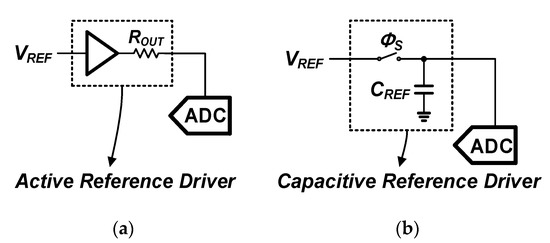
Figure 1.
Two types of analog-to-digital converter (ADC) reference driver; (a) an active reference driver and (b) a capacitive reference driver (CRD).
Since several capacitor switching schemes in the charge redistribution (CR) digital-to-analog converter (DAC) [10,11,12,13,14] have reduced the switching energy, a capacitive reference driver (CRD) utilizing a periodically charged capacitor () as a reference driver, as shown in Figure 1b, is a feasible alternative to the active reference driver with excessive power consumption. During the sampling phase (), the CRD samples an external reference voltage (). In the conversion phase, the charge redistribution takes place between the CRD and a capacitor-based digital-to-analog converter (CDAC). Thus, as the capacitor switching proceeds, the reference voltage on the CRD gradually decreases, which causes a signal-dependent error, because the switching energy is consumed differently according to the input level.
To resolve the signal-dependent reference voltage drop from a CRD during the conversion phase, there are several ways to convert the signal-dependent error to the signal-independent error, and restore it by bit weight calibration [15,16,17]. In [15], the sampling capacitor is separated from a CDAC. In [16], the auxiliary CDAC is concurrently switched to compensate the signal-dependent charge drawn from the CRD. In [17], multiple CRDs are dedicated to each capacitor in the CDAC. However, to implement bit weight calibration, additional digital logics that require additional power consumption and chip area are inevitable. In [18], the auxiliary CDAC is used to keep binary weight by compensating the reference voltage drop without a bit weight calibration, however this requires an accurate estimation of the parasitic capacitance in the CDAC. Moreover, this is only available for a few MSB capacitors, because the hardware complexity exponentially increases for a larger number of bits.
In this paper, a switched capacitive reference driver (SCRD) is introduced. During MSB conversion cycles whereby larger capacitors in a CDAC are switched, a supply voltage initially acts as a reference voltage. In the remaining LSB conversion cycles, the reference voltage connected to the CDAC is changed to a CRD from a supply voltage. Since most of the capacitor switching energy is consumed during the several MSB conversion cycles, the degree of the reference voltage’s drop in the CRD can be dramatically reduced by using the proposed SCRD, which does not require bit weight calibration or compensation requiring an auxiliary CDAC.
This paper is organized as follows. Section 2 presents the effect of the signal-dependent error of a CRD on a SAR ADC, and introduces the proposed SCRD. In Section 3, the circuit implementation of the prototype SAR ADC is described in detail. Section 4 shows the measurement results of the prototype SAR ADC to demonstrate the proposed SCRD. Finally, this paper is concluded in Section 5.
2. Proposed Switched Capacitive Reference Driver
2.1. Signal-Dependent Error of a CRD
An active reference driver has a finite output impedance (), as shown in Figure 1a. The needs to be small as the sampling frequency increases and requires more power and area to reduce . On the other hand, a CRD with a large , as shown in Figure 1b, behaves like an ideal voltage source with only metal resistance, thus improving the reference voltage settling with no static power consumption, as opposed to the active reference driver.
Despite the advantage of a low power implementation, the difficulty of using a CRD involves the signal-dependent error from charge rebalancing. To analyze the effect of the signal-dependent error of a CRD on a 12-bit SAR ADC, a behavioral simulation is performed for two popular low-energy switching schemes—the monotonic and switchback switching schemes [10,19]—and the dynamic performance comparison of the two switching schemes for various is shown in Figure 2. For the monotonic and switchback switching schemes, a doubling of improves the spurious-free dynamic range (SFDR) by about 7 dB and 6 dB, respectively. Due to the difference in switching energy, the switchback switching scheme always requires less compared to the monotonic switching scheme for the same signal-to-noise and distortion ratio (SNDR) and SFDR. For instance, a equal to achieves an SFDR of 65.8 dB and an SNDR of 64.9 dB for the switchback switching scheme, whereas the monotonic switching scheme attains an SFDR of 63.5 dB and 60.8 dB for the same . Therefore, the switchback switching scheme is utilized in our SAR ADC to reduce .
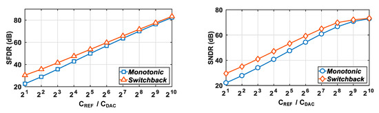
Figure 2.
The dynamic performance of a behavioral simulation for a 12-bit SAR ADC with monotonic and switchback switching schemes according to .
When using the supply as a reference voltage, the supply fluctuation from the operation of internal logics may directly degrade the performance of the SAR ADC. In addition, if the supply of the core ADC is provided by an external LDO, a huge on-chip capacitor should be required to suppress the ringing in high-speed applications due to bondwire inductance [20]. Figure 3 shows the dynamic performance of a behavioral simulation for a 12-bit SAR ADC, using the supply as the reference, according to the RMS value of supply fluctuation during the conversion phase. Assuming that supply fluctuation occurs randomly, the RMS value of the supply fluctuation should be within at least 1/2 LSB.
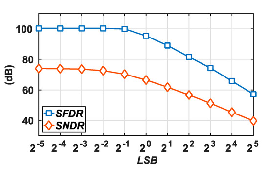
Figure 3.
The dynamic performance of a behavioral simulation for a 12-bit SAR ADC using a supply voltage as a reference voltage according to a RMS value of the supply fluctuation.
2.2. Proposed SCRD
Despite adopting the switchback switching scheme, the required for high-linearity SAR ADCs remains challenging. Thus, this paper proposes the SCRD to reduce without performance degradation. Figure 4 shows the block and timing diagram of the proposed SCRD. Each conversion cycle is identified based on the timings at which each output bit is determined after comparisons. In the total conversion cycles for -bit SAR ADC, most of the total switching energy is consumed in MSB conversion cycles, because larger capacitors are switched in upper bit conversion cycles. Thus, instead of a CRD during the MSB conversion cycles, if another kind of reference driver supplies the switching energy, the required would be reduced dramatically. Among various alternatives, a supply voltage is used to avoid static current consumption. We may define a reference switching cycle (RSC) which distinguishes a supply reference mode and a CRD mode. The later the RSC is in the conversion steps, the smaller the energy that is supplied by the CRD.
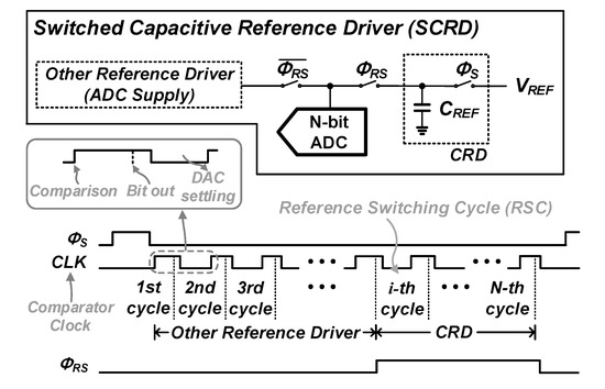
Figure 4.
The block and timing diagram of the proposed SCRD.
In the sampling phase, the supply voltage reliably acts as the reference voltage because there are no large switching activities affecting the supply fluctuation from a comparator and an SAR logic. Furthermore, the supply fluctuation affects the voltages in the differential CDAC equally, which are significantly suppressed in a differential architecture.
The switching energies supplied by the CRD with the different RSC are simulated in a 12-bit SAR ADC, and the result of this is shown in Figure 5. In other words, Figure 5 shows the total energies drawn by the CDAC from the CRD when the CRD is used from the RSC to the last cycle. The switching scheme is based on the switchback, and the effect of the signal-dependent voltage drop caused by charge sharing in the CRD is excluded to account for the worst-case maximum switching energy. Beginning with the fourth cycle, whenever the RSC increases by one cycle, the average switching energy for the CRD is reduced to approximately half. The detailed average and maximum switching energy for the CRD are summarized in Table 1. The switchback switching scheme does not consume switching energy up to the second cycle because the first cycle only performs a comparison without DAC switching. The second cycle consumes no energy due to the zero-energy DAC switching scheme, because the MSB capacitor is switched to the same voltage that the remaining LSB capacitors are connected at. The maximum switching energy for the RSC at the fifth cycle is saved by 66%, and as much as 98% of the maximum switching energy is saved for the RSC at the ninth cycle. In our design, the unit capacitance of the CDAC is 0.4 fF, and both the reference voltage and the supply voltage are 1.2 V.
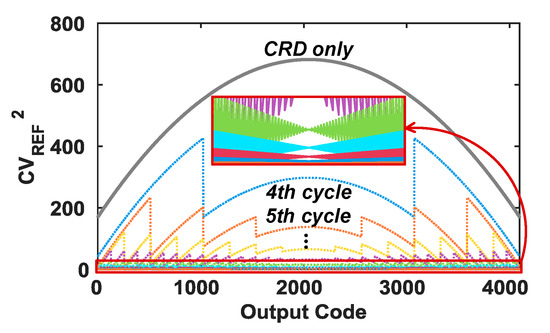
Figure 5.
The switching energy for the CRD according to the RSC.

Table 1.
Switching energy for the CRD according to the RSC.
2.3. Performance Analysis according to a RSC and CREF
In our design, two design parameters exist, which are the RSC and the . Figure 6 shows the dynamic performance of a behavioral simulation for a 12-bit SAR ADC according to and the RSC. For the RSC at the fifth and ninth cycles, the SFDR is improved by about 10.5 dB and 45 dB on average, respectively, comparing to only the CRD. Furthermore, based on the SNDR, the required is 2 and 32 times smaller compared to the CRD only for the RSC at the fifth and ninth cycles, respectively. Figure 7 shows the static performance of the behavioral simulation of the 12-bit SAR ADC according to the different schemes—the CRD only and the SCRD that has the RSCs at the fifth and ninth cycles. In this simulation, we assumed a equal to to properly reflect the actual implementation. This selection was based on the full utilization of the area under CDAC, not requiring an additional area for . Compared to only the CRD, the RSCs at the fifth and ninth cycles have less integrated non-linearity (INL) error, which is about 41 and 91% of the INL for CRD only, respectively. As the RSC increases, the INL and maximum and minimum differential non-linearity (DNL) are smaller, and the DNL plot becomes a trumpet shape that accounts for the larger switching energy variation with the input moving away from the mid-range, as shown in Figure 5.
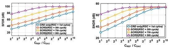
Figure 6.
SFDR and SNDR of a behavioral simulation for a 12-bit SAR ADC according to and the RSC.
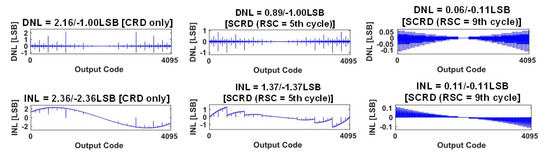
Figure 7.
DNL and INL of a behavioral simulation for a 12-bit SAR ADC according to and the RSC.
2.4. Supply-Noise Immunity of the Proposed SCRD
Although the additional current or chip area is not wasted by using a supply voltage as reference, the supply voltage is not clean enough because of the fluctuation caused by logic switching activities and cross coupling. This fluctuation might be alleviated through a large on-chip decoupling capacitor or separation into analog and digital supplies, but those methods cost area or require an additional LDO. Considering only one LDO for a SAR ADC, the major circuits that cause the supply fluctuation and ringing are the comparator and digital logics [21].
The momentary supply fluctuation affects the input voltages of the comparator through both CDACs, and leads to comparator decision error. This error is typically corrected by additional redundancy cycles just like how the incomplete DAC settling error is recovered in SAR ADCs. However, LSB conversion cycles that are not covered by the redundancy cycles are vulnerable to such external noise. In the proposed SCRD, the in a CRD is charged by a clean external reference during the sampling phase. After an RSC, the CRD takes over the role as reference, and supply noise is isolated from the CRD output, which greatly improves the supply immunity in LSB conversions.
In order to obtain the required size of the redundancy capacitor, the amount of tolerance to supply fluctuation needs to be studied in our switchback switching scheme. Assuming that the supply fluctuation with the maximum amplitude of is applied to both CDACs in each conversion cycle, the voltage difference, , between the nodes connected to the comparator inputs in both CDACs can be calculated as follows. For the first conversion cycle, the total capacitance connected to the supply voltage is the same in both CDACs in the switchback switching scheme. Therefore, for the first conversion cycle is given by
where and are the voltage variations on positive and negative CDAC, respectively. Except for the first conversion cycle, the worst of the i-th conversion cycle is when all the capacitors connected to the supply voltage are in only one side of both CDACs. Then, the worst of the i-th conversion cycle can be derived as follows:
where
In (2) and (3), is the k-th MSB capacitor in the CDAC, and is the supply voltage of the SAR ADC. Each parasitic capacitance of both CDACs is assumed to be the same, hence excluding it in (2). As the conversion cycle progresses, the becomes larger. Thus, the capacitance of the redundancy capacitor should be large enough to cover the worst at the last conversion cycle using the supply voltage as the reference driver. In the prototype SAR ADC, two redundancy cycles with a total capacitance of 72(64 + 8) are added at the 7th and 11th conversion cycles, but the first redundancy cycle is intended to compensate for incomplete DAC settling. Therefore, if the reference driver is switched to the CRD after the ninth conversion cycle, the effect of supply variation on both CDACs in the worst case is as follows.
Then, the tolerable supply fluctuation can be obtained as follows.
The redundancy capacitor of 8 can recover the supply fluctuation with an amplitude of 0.385% of the supply voltage, that is, 4.62 mV for a 1.2 V supply. If the RSC performs the two conversion cycles earlier, the tolerable supply fluctuation is improved to about 3.63% of supply (43.5 mV). Thus, in order to further suppress the supply fluctuation, we may increase the capacitance of the redundancy capacitor, or reduce the conversion cycles with the supply voltage as the reference driver
The purpose of redundancy is not to correct the reference voltage drop of the CRD, but to compensate for the decision errors caused by the incomplete CDAC settling and the noisy supply reference in MSB conversions. Such kinds of incomplete settling errors will disappear by the time the LSB conversion takes place. Thus, the additional redundancy cycles cannot reduce the error caused by the small capacitance of the CRD, which provides an incorrect reference voltages every time the CDAC switches. The required size of the CRD is only affected by the RSC because the capacitance of the switched capacitor in the CDAC, which affects charge sharing with CRD, is determined by the RSC.
2.5. Voltage Mismatch between Two Reference Voltages
In the proposed SCRD, the slight difference between the two reference voltages can be recovered by the redundancy, but it is preferable to use most of the redundancy range for correcting the decision errors before the RSC, which reduces the requirement of an on-chip decoupling capacitor to suppress the large supply fluctuation. In our design, the reference voltage of the CRD is connected to the supply voltage on the off-chip. Thus, the voltage mismatch disappears completely. Owing to the large output capacitor of the external LDO, the supply fluctuation from the supply pad is significantly restrained. In addition, the reference voltage of the CRD is quickly recovered, even when considering the effect on the bondwire inductance, because the amount of charge supplied to the CRD in the sampling phase is dramatically diminished for the SCRD. To analyze the recovery time in the CRD according to the RSC, the RLC circuit modeling bondwire inductance (), the switch resistance () and the CRD are utilized, as shown in Figure 8. The transfer function (TF) for the RLC circuit is given by
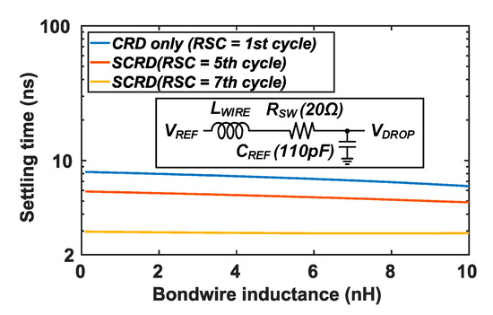
Figure 8.
Settling time of the CRD from the worst signal-dependent voltage drop according to bondwire inductance ().
Utilizing a mathematical tool, the calculated settling time for the step response of TF according to is also shown in Figure 8. Reflecting on the actual implementation values, and are fixed at 20 and 110 pF, and the calculated settling time is based on time to settle within 1/4 LSB of the SAR ADC for the worst voltage drop. For small bondwire inductance (less than 1 nH), the recovery time of the RSCs over the fifth cycle is within required time (sampling time = 6.25 ns) in our design. After the RSC at ninth cycle, the worst voltage drop of the CRD is less than 1/4 LSB, which relaxes the required recovery time significantly.
3. Circuit Implementation
The block diagram of the 12-bit SAR ADC with the proposed SCRD is shown in Figure 9. A bootstrap circuit is utilized for the top-plate sampling, and a digital logic for digital error correction (DEC) is included to obtain the typical digital output for a 12-bit ADC. To eliminate mismatch between two references in SAR ADC, the external LDO output voltage () is connected to the supply voltage () and the reference voltage of the CRD () at the off-chip with the large decoupling capacitor (, 2.2 μF), and the CDAC driver separately uses the supply voltage and the reference voltage of the CRD based on the RSC.
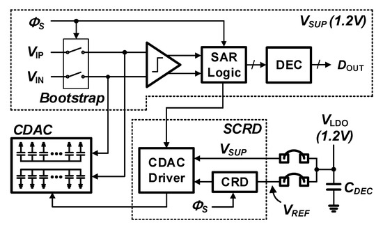
Figure 9.
The block diagram of the SAR ADC with the proposed SCRD.
3.1. Dynamic Comparator and Capacitor Switching Scheme
In typical SAR ADCs, the signal-dependent comparator kickback may affect CDAC accuracy. In order to alleviate the signal-dependent kickback from the dynamic comparator to both CDACs, the comparator architecture composed of three stages is adopted [22]. Since the first stage outputs always settle to the same voltage regardless of the input level, the effect of kickback is mitigated in the differential structure, and is regarded as offset. Moreover, the signal-dependent kickback from the dynamic latch at the last stage can be sufficiently blocked through the previous two stages.
Among various low-energy switching schemes [10,11,12,13,14], the switchback switching scheme is adopted to achieve the fast conversion time of the dynamic comparator in the upper bit conversion cycles. The dynamic comparator is composed of an N-type input pair. The first MSB capacitor is switched from ground to VREF, so a fast comparison time is achieved due to the increase in the input common-mode voltage (VCM) of the dynamic comparator. The remaining capacitors are switched from VREF to the ground, thus reducing the noise of the dynamic comparator due to the decrease in VCM [23].
An additional consideration of the switchback switching scheme is the comparator common-mode variation that causes dynamic offset. Although it can also be covered by a redundancy cycle similarly to the supply fluctuation, the requirement of the redundancy range increases. In order to estimate the redundancy range via the dynamic offset, Monte Carlo simulation is performed for various common-mode voltages in each conversion cycle, and the 1σ offsets of the dynamic comparator according to each conversion cycle are shown in Figure 10. Due to the up–down common mode voltage of the switchback switching scheme, the maximum 1σ offset is at the second conversion cycle, which has the highest common mode voltage. Considering 3σ offset as a worst case, the minimum required redundancy capacitance, , to cover the 3σ offset is as follows.
where and are the worst 1σ offset and the 1σ offset at the 14th conversion cycle. is an LSB voltage. At the seventh conversion cycle as in the first redundancy cycle, the minimum required capacitance of the first redundancy capacitor is determined by the 1σ offset at the second conversion cycle, and is calculated to be about 5.4, which occupies about 8.5% of a redundancy range for the first redundancy capacitor (64). Similarly, 1σ offset at the 7th conversion cycle is the worst offset between the 7th and 11th conversion cycles, so the minimum required capacitance of the second redundancy capacitor is about 0.3, which occupies only 3.75% of the redundancy range covered by the second redundancy capacitor (8). The dynamic offset occupies just 8% of the total redundancy range in our implementation. The dynamic offset for the last four conversion cycles is not covered by redundancy conversion cycles, but it is small and negligible.
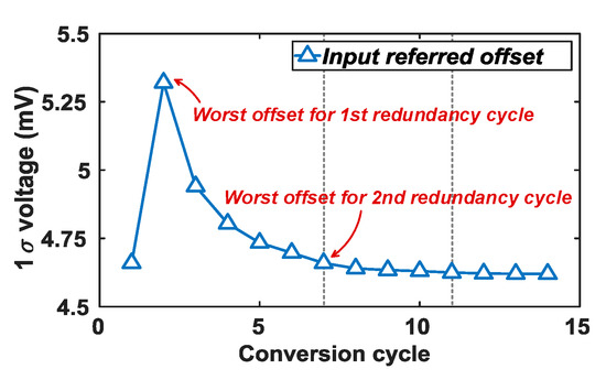
Figure 10.
The block diagram of the SAR ADC with the proposed SCRD.
3.2. SAR Logic
Figure 11 shows the block and timing diagram of the asynchronous SAR logic. After the sampling phase , activates the first sequence enable circuit (SEC), as shown in Figure 12. After the first comparison, COMP_DONE goes to high and acts as an enable signal (EN[0]) that activates a latch to transfer the comparator output to the CDAC driver. At the falling edge of COMP_DONE, the shift register transfers to SEQ[0], and activates the second SEC while stopping the first SEC. This sequence is repeated until the end of the conversion cycles. When STANDBY is high and DONE is low, each SEC passes COMP_DONE to EN with only one logic delay of the AND gate.
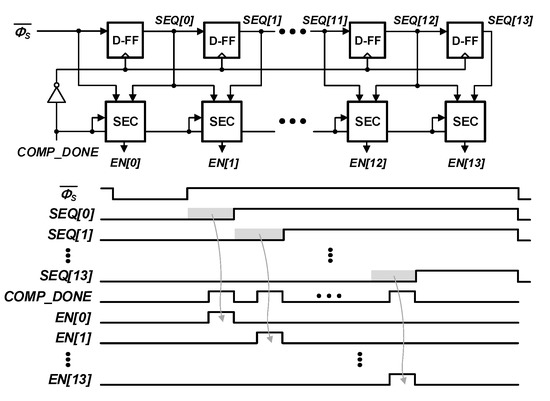
Figure 11.
The block and timing diagram of the asynchronous SAR logic.
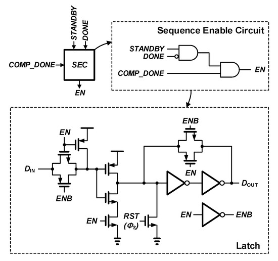
Figure 12.
The schematic of the sequence enable circuit (SEC) and latch.
3.3. Layout of the CDAC and CRD
Figure 13 shows the layout of the CDAC. The unit capacitance of the CDAC is 0.4 fF, which leads to a total capacitance of about 850 fF, including two redundancy capacitors (25.6 Ff + 3.2 fF). The CDAC consists of a custom metal-oxide–metal (MOM) capacitor with an upper metal layer to minimize the parasitic capacitance from the substrate. The CRD is located under the CDAC to eliminate the additional chip area, and is implemented with MOS capacitors to maximize for the given area. The total capacitance of the CRD is 110 pF, which is about 27 times larger than .
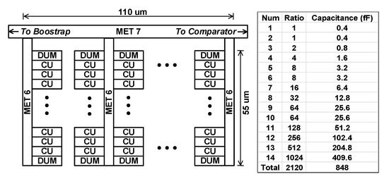
Figure 13.
The layout of the CDAC with the CRD using MOS capacitors.
The parasitic capacitors on the outputs of the CDAC drivers should be minimized to prevent further voltage drop in the reference voltage. As the influence of this parasitic capacitor is shown along with the switching of the capacitors in the CDAC, such a voltage drop is also signal-dependent. Figure 14 shows the SFDR of a behavioral simulation for a 12-bit SAR ADC with CRD only, according to the total capacitance of parasitic capacitors ( = ). Each capacitance of the parasitic capacitors () is assumed to be , where is . For a equal to , the SFDR is degraded by 1 dB and 1.7 dB for of 0.3 and 0.5, respectively. In the switchback switching scheme with up–down transition, the draws the charge from only in the first conversion cycle that makes the upward switching transition in the reference connection. On the other hand, in the remaining conversion cycles, only a downward switching transition is used, which eliminates the interaction between and . Therefore, the proposed SCRD can remove the additional reference drop caused by the MSB parasitic capacitor for the RSC at the third cycle or higher.
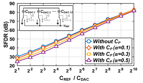
Figure 14.
SFDR of a behavioral simulation of a 12-bit SAR ADC with the CRD only according to the total capacitance of parasitic capacitors (CP).
3.4. CDAC Drivers
Figure 15 shows the schematic of the CDAC drivers implementing the proposed SCRD. During the several MSB conversion cycles, the supply voltage acts as the reference voltage using the stacked P-type MOS transistors (M1 and M2) of the each CDAC driver. The turn-on resistance and W/L of each of the P-type MOS transistors (M1-M4) are 30 and 64 u/0.065 u, whereas the flipped voltage follower in [24] would consume more than 1 mA to make 30. The added switch provides a sufficiently small turn-on resistance. After the -th conversion cycle, SEQ[-1] goes to high and waits for the next conversion cycle. Then, at the following conversion cycle named RSC, EN switches the reference voltage from the supply voltage to the VREF of the CRD until all conversion cycles are complete. In the prototype SAR ADC, the RSC is at the ninth cycle. Meanwhile, to prevent glitches during DAC settling, the EN is directly connected to an OR gate for securing the margin of the latch delay.
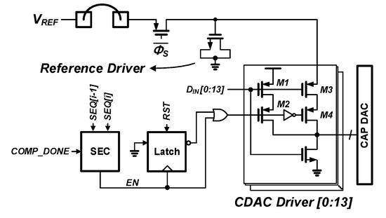
Figure 15.
The schematic of the CDAC drivers with the CRD.
4. Measurement Results
The prototype SAR ADC is fabricated in a 65 nm CMOS process and occupies 0.0448 mm2 without the additional area of the CRD, as shown in Figure 16. The supply voltage is only 1.2 V, and the power consumption is 1.1 mW, including the power consumed by the CRD during the sampling phase.
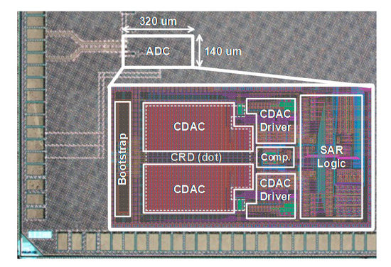
Figure 16.
Die photograph.
Figure 17 shows the measured dynamic performance of the SAR ADC with an SCRD for a sampling frequency ranging from 5 MHz to 40 MHz. With the SCRD, the SAR ADC achieves at least an SFDR of 80 dB and an SNDR of 66.3 dB. The measured frequency spectra of the SAR ADC, with an SCRD using the input frequencies of nearly 0.987 MHz and 19.67 MHz, are shown in Figure 18. Even if the input frequency approaches the Nyquist frequency, the SNDR reduction is about 2 dB. At a near-Nyquist input frequency, the SFDR with the SCRD is 80.6 dB. Thus, from Figure 13, we can see that the SCRD improves the SFDR by about 16 dB compared to the CRD only, where the and are 0.3 and , respectively.
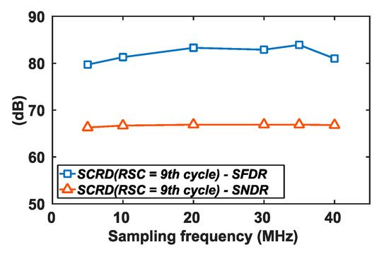
Figure 17.
The measured dynamic performance of the SAR ADC with the SCRD according to the sampling frequency.
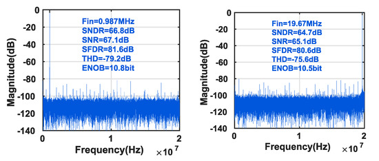
Figure 18.
The measured frequency spectrum of the SAR ADC with the SCRD at near 1 MHz and 20 MHz input frequency.
The signal-dependent error of the SCRD can be monitored by DNL and INL. With the SCRD, the measured maximum and minimum DNL and INL are 0.71/−0.4 LSB and 0.8/−1.08 LSB, respectively, as shown in Figure 19. The INL is limited to the capacitor mismatch of the CDAC, especially for an MSB capacitor. Except for the effect of the capacitor mismatch, the measured DNL plot has a trumpet shape because the degree of reference voltage drop in the CRD is largely changed with the input away from the mid-code. However, the DNL error caused by the reference voltage drop is less than 0.5/−0.5 LSB.
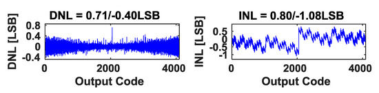
Figure 19.
The measured DNL and INL of the SAR ADC with the SCRD.
Figure 20 shows the measurement setup for observing the ADC performance according to the supply fluctuation with an amplitude of VAMP. The bias tee of Mini-Circuits combines the interference signals with a 1.2 V supply voltage from Agilent E3631A. The frequencies of the interference signals of Agilent E4438C are chosen such that the frequencies are not sub-multiples of the sampling or input frequency. Furthermore, in order to observe only the effect of the internal supply fluctuation, the reference voltage connected to the CRD is supplied stably by another external LDO. Utilizing this measurement setup, the dynamic performance of the SAR ADC is measured for the supply reference and the SCRD by varying VAMP, as shown in Figure 21. Owing to the redundancy cycle, the dynamic performance of the SCRD maintains up to 25 mV for the VAMP, while using the supply reference only, and has no tolerance to the noise with increasing VAMP. If the RSC moves to a lower bit, the tolerable supply fluctuation is reduced because the effect of the supply fluctuation dominates at the bit conversion cycle that is lower than (2).
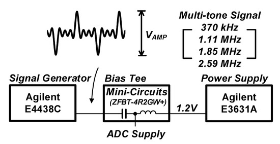
Figure 20.
The measurement setup to observe the effect of the supply fluctuation on the dynamic performance of the SAR ADC.
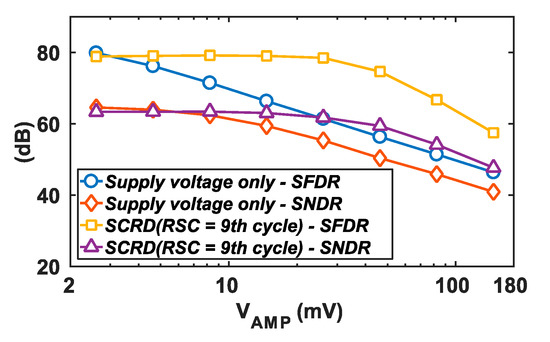
Figure 21.
The measured dynamic performance of the prototype SAR ADC for the supply reference and the SCRD by varying VAMP.
Table 2 summarizes the overall performance of the SAR ADC with the SCRD and other SAR ADCs. The SAR ADC with the SCRD achieves an SFDR of 81.6 dB and an effective number of bits (ENOB) of 10.46 at the Nyquist input frequency without bit weight calibration or compensation utilizing an auxiliary CDAC, which leads to a figure-of-merit (FOM) of 19.59 fJ/conversion step. The achieved peak SFDR is the highest if we consider no bit weight calibration involved. The power consumption for the reference driver is only 7.4 μW, which consumes only CDAC switching energy. Compared to other SAR ADCs with CRD, the proposed SCRD consumes the least power due to its structure without an auxiliary CDAC for compensating for reference voltage drop, or a digital circuit for bit weight calibration. Although a slightly larger size of CRD with the capacitance of 110 pF is used, the SAR ADC with the SCRD occupies the smallest area owing to the location of the CRD under the CDAC utilizing the MOS capacitors. Furthermore, by including the redundancy capacitors implemented in our design, an SFDR of 80 dB can be obtained by the CRD with 14 repetitions of CDAC for the SCRD, which means the additional area for the CRD is small even if the MOS capacitor is not used under the CDAC. In our implementation, an additional conversion cycle is allocated for redundancy to compensate for errors caused by supply fluctuation, which increases conversion time. Thus, for high-speed applications, a non-binary search algorithm can be considered to reduce the additional cycle [25].
Table 2.
Performance summary and comparison.
5. Conclusions
This paper presents a switched capacitive reference driver (SCRD). During several MSB conversion cycles, a supply voltage acts as a reference voltage and provides most of the switching energy to the CDAC. From an RSC, the CRD offers a reference voltage instead of the supply voltage, with less signal-dependent error owing to the small switching energy during the lower bit conversion cycles. From the measurement, we see that a prototype SAR ADC achieves an SNDR and an SFDR of 64.7 dB and 80.6 dB, respectively. The SAR ADC consumes 1.1 mW at Nyquist input frequency, which leads to an FOM of 19.59 fJ/conversion step.
Author Contributions
Conceptualization, H.J.; Data curation, H.J.; Formal analysis, H.J.; Funding acquisition, M.L.; Investigation, S.L.; Methodology, H.J.; Project administration, M.L.; Supervision, M.L.; Visualization, H.J.; Writing—original draft, H.J.; Writing—review & editing, H.J. All authors have read and agreed to the published version of the manuscript.
Funding
This work was supported in part by the National Research Foundation of Korea (NRF) Grant funded by the Korean Government (MEST) (No. 2019R1A2B5B01069415) and by the Future Interconnect Technology Cluster Program of Samsung Electronics. The EDA tools were supported by IDEC, Korea.
Conflicts of Interest
The authors declare no conflict of interest.
References
- Lu, T.C.; Van, L.D.; Lin, C.S.; Huang, C.M. A 0.5 V 1 KS/s 2.5 nW 8.52-ENOB 6.8 fJ/conversion-step SAR ADC for biomedical applications. In Proceedings of the IEEE Custom Integrated Circuits Conference (CICC), San Jose, CA, USA, 19–21 September 2011; pp. 1–4. [Google Scholar]
- Chen, Y.J.; Chang, K.H.; Hsieh, C.C. A 2.02-5.16 fJ/conversion step 10 bit hybrid coarse-fine SAR ADC with time-domain quantizer in 90 nm CMOS. IEEE J. Solid State Circuits 2016, 51, 357–364. [Google Scholar]
- Frans, Y.; Shin, J.; Zhou, L.; Upadhyaya, P.; Im, J.; Kireev, V.; Elzeftawi, M.; Hedayati, H.; Pham, T.; Asuncion, S. 56-Gb/s PAM4 wireline transceiver using a 32-way time-interleaved SAR ADC in 16-nm FinFET. IEEE J. Solid State Circuits 2017, 52, 1101–1110. [Google Scholar] [CrossRef]
- Kundu, S.; Alpman, E.; Lu, J.H.L.; Lakdawala, H.; Paramesh, J.; Jung, B.; Zur, S.; Gordon, E. A 1.2 V 2.64 GS/s 8 bit 39 mW skew-tolerant time-interleaved SAR ADC in 40 nm digital LP CMOS for 60 GHz WLAN. IEEE Trans. Circuits Syst. I Regul. Pap. 2015, 62, 1929–1939. [Google Scholar] [CrossRef]
- Xu, H.; Huang, H.; Cai, Y.; Du, L.; Zhou, Y.; Xu, B.; Gong, D.; Ye, J.; Chiu, Y. A 78.5-dB SNDR radiation-and metastability-tolerant two-step split SAR ADC operating up to 75 MS/s with 24.9-mW power consumption in 65-nm CMOS. IEEE J. Solid State Circuits 2018, 54, 441–451. [Google Scholar] [CrossRef]
- Inerfield, M.; Kamath, A.; Su, F.; Hu, J.; Yu, X.; Fong, V.; Alnaggar, O.; Lin, F.; Kwan, T. An 11.5-enob 100-ms/s 8mw dual-reference sar adc in 28 nm cmos. In Proceedings of the IEEE Symposium on VLSI Circuits Digest of Technical Papers, Honolulu, HI, USA, 10–13 June 2014; pp. 1–2. [Google Scholar]
- Shen, Y.; Tang, X.; Shen, L.; Zhao, W.; Xin, X.; Liu, S.; Zhu, Z.; Sathe, V.S.; Sun, N. A 10-bit 120-MS/s SAR ADC with reference ripple cancellation technique. IEEE J. Solid State Circuits 2019, 55, 680–692. [Google Scholar] [CrossRef]
- Huang, G.Y.; Chang, S.J.; Liu, C.C.; Lin, Y.Z. A 1-µW 10-bit 200-kS/s SAR ADC with a bypass window for biomedical applications. IEEE J. Solid State Circuits 2012, 47, 2783–2795. [Google Scholar] [CrossRef]
- Harpe, P.; Cantatore, E.; van Roermund, A. A 10b/12b 40 kS/s SAR ADC with data-driven noise reduction achieving up to 10.1 b ENOB at 2.2 fJ/conversion-step. IEEE J. Solid State Circuits 2013, 48, 3011–3018. [Google Scholar] [CrossRef]
- Liu, C.C.; Chang, S.J.; Huang, G.Y.; Lin, Y.Z. A 10-bit 50-MS/s SAR ADC with a monotonic capacitor switching procedure. IEEE J. Solid State Circuits 2010, 45, 731–740. [Google Scholar] [CrossRef]
- Zhu, Z.; Xiao, Y.; Song, X. V CM-based monotonic capacitor switching scheme for SAR ADC. Electron. Lett. 2013, 49, 327–329. [Google Scholar] [CrossRef]
- Hariprasath, V.; Guerber, J.; Lee, S.H.; Moon, U.K. Merged capacitor switching based SAR ADC with highest switching energy-efficiency. Electron. Lett. 2010, 46, 620–621. [Google Scholar] [CrossRef]
- Osipov, D.; Paul, S. Two advanced energy-back SAR ADC architectures with 99.21 and 99.37% reduction in switching energy. Analog. Integr. Circuits Signal. Process. 2016, 87, 81–91. [Google Scholar] [CrossRef]
- Sanyal, A.; Sun, N. SAR ADC architecture with 98% reduction in switching energy over conventional scheme. Electron. Lett. 2013, 49, 248–250. [Google Scholar] [CrossRef]
- Kapusta, R.; Shen, J.; Decker, S.; Li, H.; Ibaragi, E.; Zhu, H. A 14b 80 ms/s sar adc with 73.6 db sndr in 65 nm cmos. IEEE J. Solid State Circuits 2013, 48, 3059–3066. [Google Scholar] [CrossRef]
- Martens, E.; Hershberg, B.; Craninckx, J. A 69-dB SNDR 300-MS/s two-time interleaved pipelined SAR ADC in 16-nm CMOS FinFET with capacitive reference stabilization. IEEE J. Solid State Circuits 2018, 53, 1161–1171. [Google Scholar] [CrossRef]
- Shen, J.; Shikata, A.; Fernando, L.D.; Guthrie, N.; Chen, B.; Maddox, M.; Mascarenhas, N.; Kapusta, R.; Coln, M.C.W. A 16-bit 16-MS/s SAR ADC with on-chip calibration in 55-nm CMOS. IEEE J. Solid State Circuits 2018, 53, 1149–1160. [Google Scholar] [CrossRef]
- Liu, M.; van Roermund, A.H.; Harpe, P. A 10-b 20-MS/s SAR ADC with DAC-compensated discrete-time reference driver. IEEE J. Solid State Circuits 2018, 54, 417–427. [Google Scholar] [CrossRef]
- Huang, G.Y.; Chang, S.J.; Liu, C.C.; Lin, Y.Z. 10-bit 30-MS/s SAR ADC using a switchback switching method. IEEE Tran. Very Large Scale Integr. (VLSI) Syst. 2012, 21, 584–588. [Google Scholar] [CrossRef]
- Li, C.; Chan, C.H.; Zhu, Y.; Martins, R.P. Analysis of reference error in high-speed SAR ADCs with capacitive DAC. IEEE Trans. Circuits Syst. I Regul. Pap. 2018, 66, 82–93. [Google Scholar] [CrossRef]
- Liu, W.; Huang, P.; Chiu, Y. A 12-bit, 45-MS/s, 3-mW redundant successive-approximation-register analog-to-digital converter with digital calibration. IEEE J. Solid State Circuits 2011, 46, 2661–2672. [Google Scholar] [CrossRef]
- Jeon, H.; Kim, Y.B. A novel low-power, low-offset, and high-speed CMOS dynamic latched comparator. Analog. Integr. Circuits Signal Process. 2012, 70, 337–346. [Google Scholar] [CrossRef]
- Hu, Y.S.; Shih, C.H.; Tai, H.Y.; Chen, H.W.; Chen, H.S. A 0.6 V 6.4 fJ/conversion-step 10-bit 150 MS/s subranging SAR ADC in 40 nm CMOS. In Proceedings of the IEEE Asian Solid-State Circuits Conference (A-SSCC), KaoHsiung, Taiwan, 10–12 November 2014; pp. 81–84. [Google Scholar]
- Chan, C.H.; Zhu, Y.; Li, C.; Zhang, W.H.; Ho, I.M.; Wei, L.; Seng-Pan, U.; Martins, R.P. 60-dB SNDR 100-MS/s SAR ADCs with threshold reconfigurable reference error calibration. IEEE J. Solid State Circuits 2017, 52, 2576–2588. [Google Scholar] [CrossRef]
- Li, D.; Zhu, Z.; Ding, R.; Yang, Y. A 1.4-mW 10-bit 150-MS/s SAR ADC with nonbinary split capacitive DAC in 65-nm CMOS. IEEE Trans. Circuits Syst. II Express Briefs 2017, 65, 1524–1528. [Google Scholar] [CrossRef]
- Zhu, Y.; Chan, C.H.; Chio, U.F.; Sin, S.W.; Seng-Pan, U.; Martins, R.P.; Maloberti, F. A 10-bit 100-MS/s reference-free SAR ADC in 90 nm CMOS. IEEE J. Solid State Circuits 2010, 45, 1111–1121. [Google Scholar] [CrossRef]


Publisher’s Note: MDPI stays neutral with regard to jurisdictional claims in published maps and institutional affiliations. |
© 2020 by the authors. Licensee MDPI, Basel, Switzerland. This article is an open access article distributed under the terms and conditions of the Creative Commons Attribution (CC BY) license (http://creativecommons.org/licenses/by/4.0/).