Abstract
This paper presents a low-complexity address generation unit (AGU) for multiuser detectors in interleave division multiple access (IDMA) systems. To this end, for the first time, all possible options for designing AGUs are first analyzed in detail. Subsequently, a complexity reduction technique is applied to each of those architectures. More specifically, some components in AGUs are relocated to make them shareable and removable without affecting the functionality. The complete transparency of such renovation makes it applicable to any existing multiuser detector without tailoring the interfacing components therein. Measuring the hardware complexity, all the resulting AGUs are compared with each other, and a new architecture simpler than the state-of-the-art one is developed. Implementation results in a 65 nm CMOS process, demonstrating that the proposed AGU can alleviate the equivalent gate count and the power consumption of the prior process by 13% and 31%, respectively.
1. Introduction
Nonorthogonal multiple access (NOMA) is an emerging class of multiple-access technologies in 5G telecommunications and the Internet of Things [1]. Interleave division multiple access (IDMA) is one of the NOMA schemes that distinguishes multiple users according to their distinct interleaving patterns [2]. By virtue of its fine scalability and robustness, IDMA is considered as a promising NOMA candidate for the forthcoming applications [3].
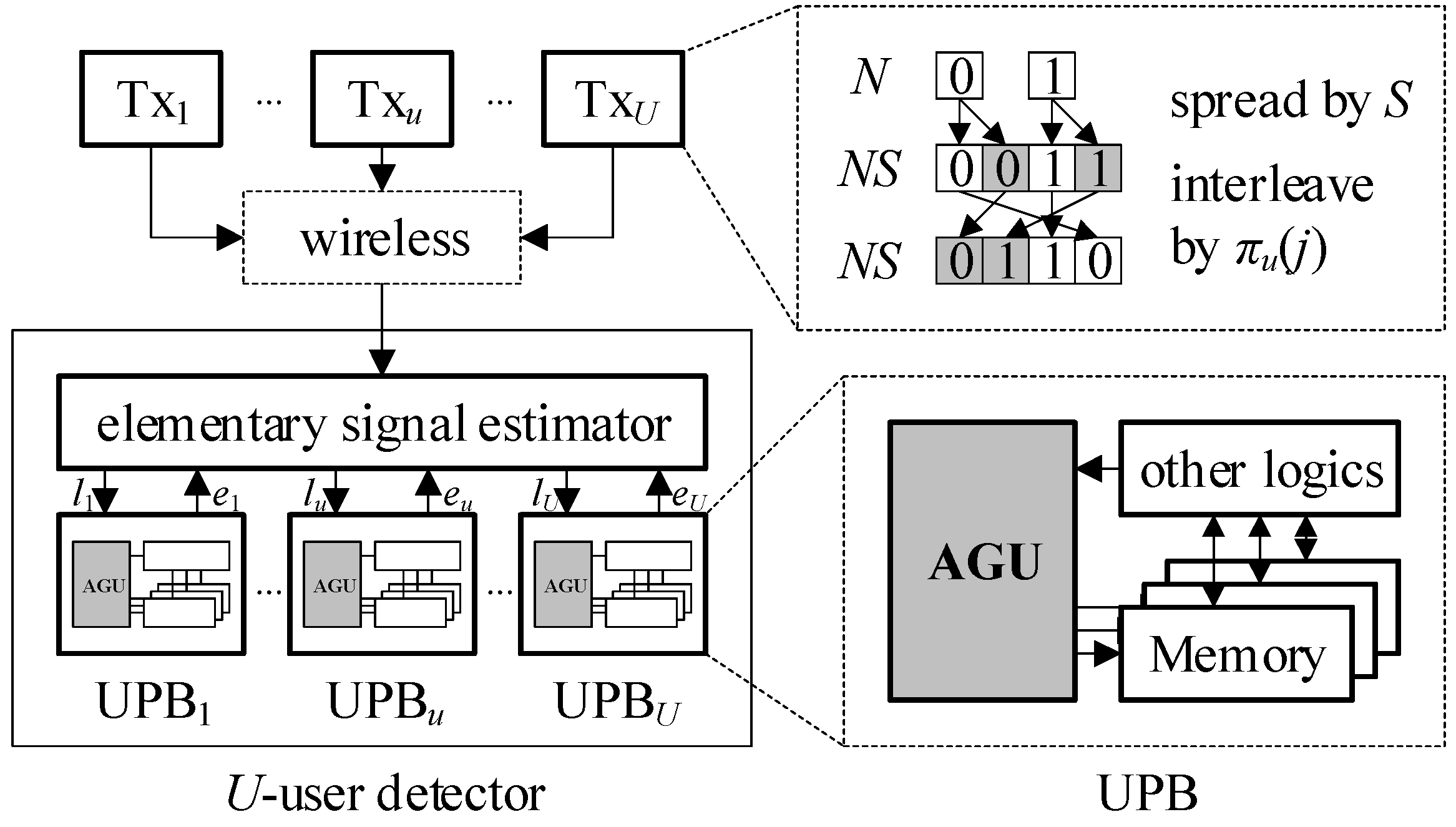
Recent works in the literature have pioneered sophisticated multiuser detector architectures for IDMA systems [4,5,6,7,8,9,10,11]. As generalized in Figure 1, a U-user detector incorporates U user-wise processing blocks (UPBs) and one elementary signal estimator (ESE). Each UPB contains its own address generation unit (AGU) for accessing memories therein. Since all users employ distinct interleaving patterns and access memories in their own manners, all the U AGUs are implemented separately, making the total number of AGUs in a detector U. Accordingly, when a massive number of users are connected, i.e., U >> 1, the AGUs as a whole contribute a significant portion to the overall hardware complexity.

Figure 1.
Interleave division multiple access (IDMA) system and U-user detector architecture.
Despite the weightiness in implementation, only one AGU structure [5] has been presented in the literature, and it has never been studied in detail. For the first time, this paper analyzes all possible options for designing AGUs, and then a complexity reduction technique is applied to each of those architectures. More specifically, some components in AGUs are relocated to make them shareable and removable without affecting the functionality. The complete transparency of such renovation makes it applicable to any existing multiuser detector without tailoring the interfacing components therein. Measuring the hardware complexity, all the resulting AGUs are compared with each other, and a new architecture simpler than the state-of-the-art one is developed. Implementation results in a 65 nm CMOS process that will demonstrate that the proposed AGU can alleviate the equivalent gate count and the power consumption of the prior process by 13% and 31%, respectively.
The rest of this paper is organized as follows. Section 2 reviews the fundamentals of multiuser detection in IDMA systems. Section 3 compares two addressing modes for AGUs. The proposed complexity reduction technique is presented in Section 4. In Section 5, all possible options for AGUs are evaluated and discussed along with the implementation results. Concluding remarks are made in Section 6.
2. Background
At the transmitter of the uth user (Txu) in Figure 1, each of N information bits is first replicated S times by a spreader. The resulting sequence of J = NS chips is then permuted by an interleaver of length J. The sequences of the J chips before and after interleaving can be indexed by {j} and {πu(j)}, respectively, for j = 0, 1, …, J – 1. πu(∙) is the interleaving function of the uth user. In case of J = 4 and U = 2, for example, {j} = {0, 1, 2, 3}, {π1(j)} = {2, 0, 3, 1}, and {π2(j)} = {1, 3, 2, 0}. Note that two interleaving patterns are distinct. The chips departing from U users go through a wireless channel while interfering with each other. In a multiuser detector receiving the chips with interference, the ESE first distributes lu(πu(j)) to UPBu for u = 1, 2, …, U, where lu(πu(j)) is the log-likelihood ratio (LLR) of the jth chip from the uth user. In return, UPBu answers the ESE with eu(πu(j)), called an extrinsic LLR. After the ESE and UPBs exchange their LLRs several times, the final estimates of the N information bits are determined by the signs of LLRs.
The operation of UPBu can be formulated for all j = 0, 1, …, J – 1 as
du(pu(j)) is called a despread LLR, and pu(j) is the index of the despread LLR that corresponds to lu(πu(j)). Accordingly, the first line of (1) states that an extrinsic LLR, eu(πu(j)), is calculated by subtracting an incoming LLR, lu(πu(j)), from its corresponding despread LLR, du(pu(j)). Comparing the first and the second lines of (1) suggests that du(pu(j)) is the sum of S LLRs associated with pu(j). Since pu(j) = floor(πu(j)/S), as rewritten in the third line of (1), {πu(j)} can be divided into J/S disjoint subsets, each of which has S elements associated with the same pu(j). Then, du(pu(j)) can be interpreted as the sum of such S LLRs in a subset. Let us exemplify with J = 4, S = 2, and {πu(j)} = {2, 3, 1, 0}. The elements in subset {πu(0), πu(1)} = {2, 3} are associated with pu(j) = 1, and du(pu(j)) = du(1) is the sum of S = 2 LLRs, lu(2) + lu(3). The elements in subset {πu(2), πu(3)} = {1, 0} are related with pu(j) = 0, and du(pu(j)) = du(0) = lu(1) + lu(0). It is worth noting that obtaining one despread LLR by accumulating S LLRs associated with the same pu(j) is the inverse of spreading that makes S replicas of the pu(j)-th information bit.
The state-of-the-art scheme to calculate (1), which is called on-the-fly despreading [5], has dominantly been employed by the latest UPBs [5,6,7,8]. It comprises two phases: 1) reception and 2) response. In the first phase, UPBu receives lu(πu(j)) for all j = 0, 1, …, J – 1 from the ESE, and stores them into a memory named ML. Simultaneously, it adds lu(πu(j)) to the pu(j)-th entry in a memory named MP1. MP1 contains J/S entries, each of which corresponds to a partial sum (PS) of du(pu(j)). After accumulating all the J LLRs as stated, the PSs become {du(pu(j))}. Let us exemplify again with J = 4, S = 2, {πu(j)} = {2, 3, 1, 0}, du(0) = lu(0) + lu(1), and du(1) = lu(2) + lu(3).
- (1)
- For j = 0, lu(2) is stored into ML, and the PS of du(1) in MP1 is set to lu(2).
- (2)
- For j = 1, lu(3) is stored into ML, and the PS of du(1) in MP1, which has been lu(2), is updated to du(1) = lu(2) + lu(3).
- (3)
- For j = 2, lu(1) is stored into ML, and the PS of du(0) in MP1 is set to be lu(1).
- (4)
- For j = 3, lu(0) is stored into ML, and the PS of du(0) in MP1, which has been lu(1), is updated to du(0) = lu(1) + lu(0).
As a result of J = 4 cycles, {lu(πu(j))} and {du(pu(j))} have been prepared in ML and MP1, respectively. In the second phase, UPBu returns eu(πu(j)) = du(pu(j)) – lu(πu(j)) to the ESE for all j = 0, 1, …, J – 1. The minuend and the subtrahend are retrieved from MP1 and ML, respectively. The next reception phase in which new PSs are to be computed may start in the middle of the response phase. However, since {du(pu(j))} in MP1 are in use during the response phase, they should not be overwritten. Accordingly, the new PSs are stored into a duplicate memory of MP1, named MP2. As the phases iterate, the roles of MP1 and MP2 alternate. For example, in even-numbered iterations, MP1 provides du(pu(j)), while MP2 manages new PSs. In odd-numbered iterations, vice versa.
3. AGUs Based on Sequential and Interleaved Addresses
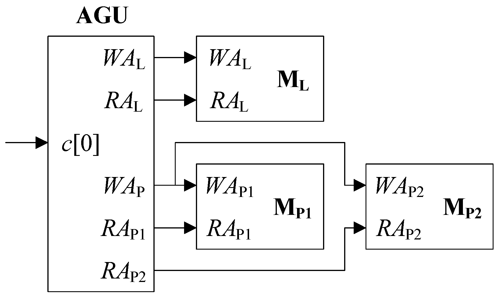
As stated above, every UPB intensively accesses ML, MP1, and MP2 every cycle to read and write LLRs and PSs, necessitating the generation of proper read and write addresses. The AGU is responsible for organizing such addresses, and interfaces with the memories as depicted in Figure 2. The nomenclature of the signals is as follows. The baseline text stands for the functionality of an address, while the subscript designates the memory associated. For example, RAL is the read address for ML, and WAL is the write address for ML. In a similar manner, RAP1, RAP2, WAP1, and WAP2 are the read and write addresses for MP1 and MP2, respectively. Note that both MP1 and MP2 take WAP as their common write address. c[0] is the least significant bit (LSB) of the current iteration count c, it being 1 if the current iteration is odd-numbered or 0 if even-numbered. Table 1 briefs the meanings as a prompt reference.

Figure 2.
Interface between address generation unit (AGU) and memories.

Table 1.
List of signals.
Let us recapitulate that ML has J entries to store lu(πu(j)) for j = 0, 1, …, J – 1, and each of MP1 and MP2 has J/S entries to hold PSs of du(pu(j)) for pu(j) = 0, 1, …, J/S – 1. While pu(j) is the only addressing scheme for J/S entries of MP1 and MP2, two different options are available for accessing the J entries of ML. One is to use sequential addresses (SAs), {j}, and the other is to adopt interleaved addresses (IAs), {πu(j)}. Nevertheless, only the former has been presented in the literature [5], and it has never been compared with the latter.
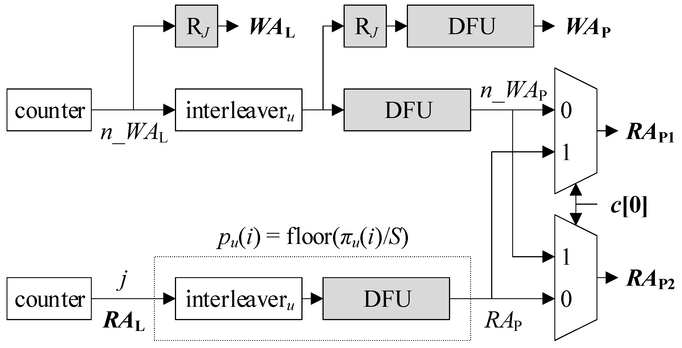
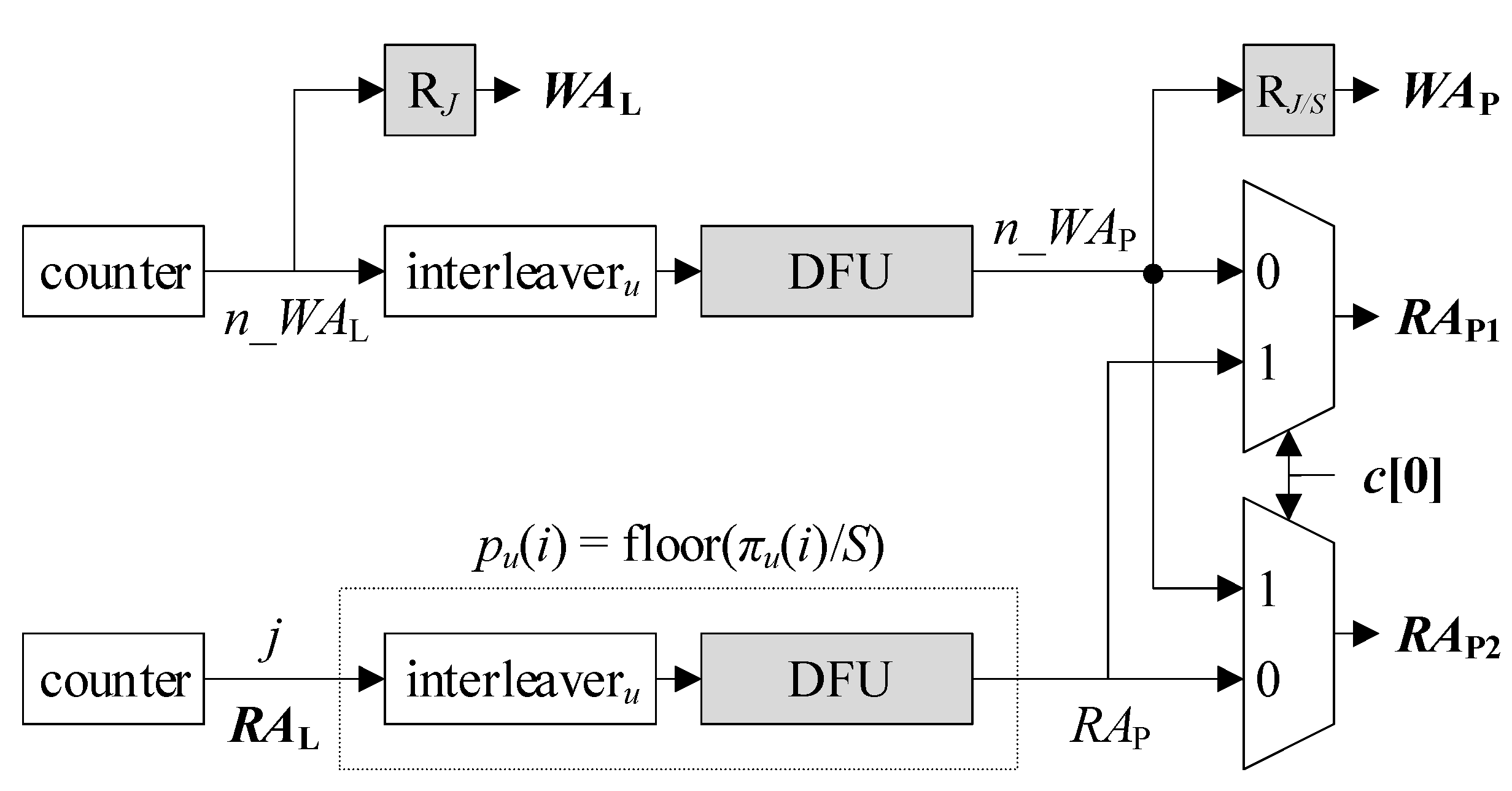
Figure 3 sketches the existing AGU using SAs [5]. The output of the counter at the bottom, which is a cyclic sequence of elements in {j} = {0, 1, …, J – 1}, is readily used as RAL. The output of the other counter at the top, which precedes the bottom one by E – 1 cycles, plays the role of n_WAL. n_WAL is the next write address for ML that precedes WAL by one cycle, and E is the latency of the ESE. RJ denotes a D-type register holding log2J bits, where the subscript J represents the argument of the logarithm. Both RAL and WAL are log2J-bit long so as to address all J entries in ML. WAL is generated by RJ that defers n_WAL one cycle. Given i as input, interleaveru makes πu(i). Given i as input, a division-by-S-and-floor unit (DFU) calculates floor(i/S). Putting it all together, given RAL or j as input, a series of interleaveru and a DFU bounded by dotted lines derives RAP = floor(πu(j)/S) = pu(j). RAP serves as one input of each multiplexer. By the other set of interleaveru and the following DFU, n_WAL is transformed into n_WAP, which fills the remaining input of each multiplexer. According to c[0], RAP1 and RAP2 alternate between n_WAP and RAP. This implements the aforementioned role exchange of MP1 and MP2, i.e., one retrieves du(pu(j)) to compute eu(πu(j)) in the response phase, while the other prefetches a PS to accumulate lu(πu(j)) during the reception phase. A series of RJ and a DFU that follows the upper interleaveru makes WAP.
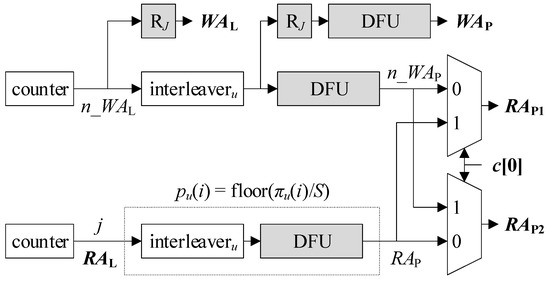
Figure 3.
Sequential-address-based AGU (S-AGU).
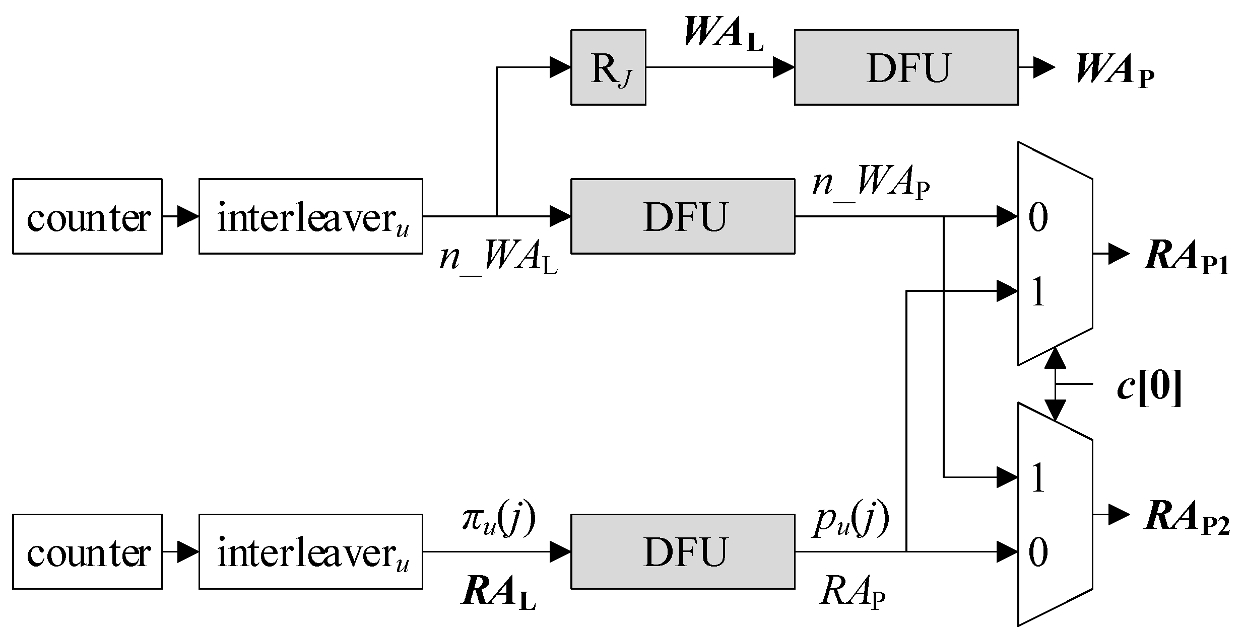
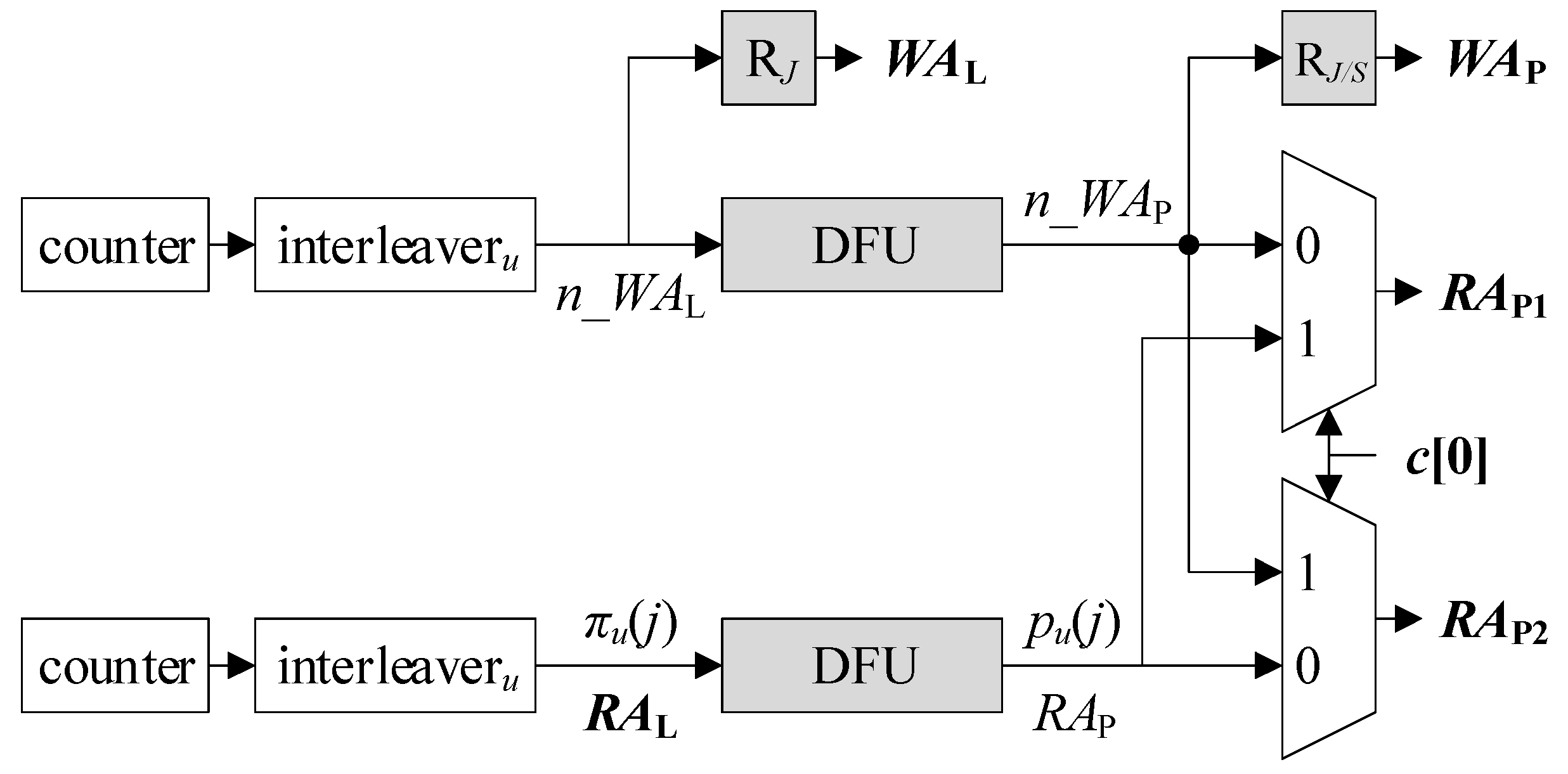
On the other hand, Figure 4 depicts another possible AGU that uses IAs. Unlike the SA-based AGU (S-AGU), RAL is the output of interleaveru that shuffles a cyclic sequence from a counter {j}, i.e., {πu(j)}. n_WAL is also taken from the output of the other interleaveru. The two counters are out of phase by E – 1 cycles as they are in Figure 3. Since RAL is already an IA, a DFU is the only remaining stage to be undergone ahead of RAP. Similarly, n_WAP is made by a DFU that takes n_WAL as input. n_WAP and RAP are connected to the multiplexers.
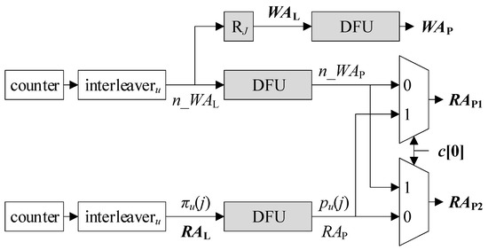
Figure 4.
Interleaved-address-based AGU (I-AGU).
Both AGUs in Figure 3 and Figure 4 contain two counters, two interleavers, and two multiplexers. Excluding such ones in common, the remaining components are colored grey for emphasis. The IA-based AGU (I-AGU) has one less RJ than the S-AGU. On the other hand, since SAs in {j} are independent of u unlike the IAs in {πu(j)}, the counters and RJ that generate RAL and WAL can be shared among all UPBu for u = 1, 2, …, U, being an advantage of the S-AGU. Another noteworthy merit of the S-AGU is that it may employ the simplified memory subsystem in Ref. [7]. More specifically, ML is usually implemented with a dual-port memory to accommodate two requests per cycle. When ML is accessed by SAs, however, a pair of adjacent requests can be integrated into one, and the number of memory accesses per cycle is reduced from two to one. Then, ML can be implemented with a single-port memory instead of a dual-port one, reducing the hardware complexity significantly.
4. DFU-Reduced Architecture
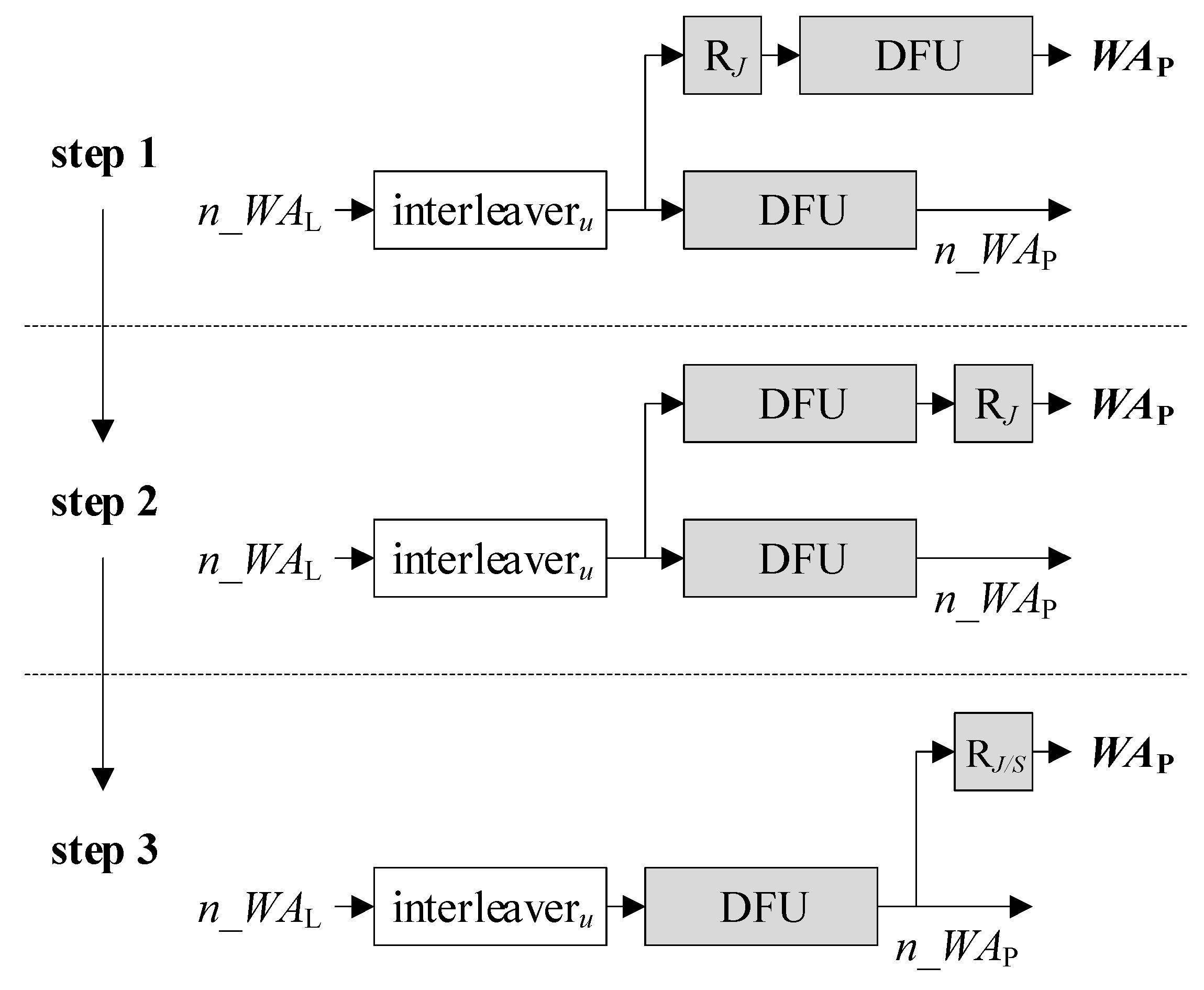
A DFU includes a division that incurs a significant hardware burden. It is therefore important to minimize the number of DFUs. To this end, we now manipulate the AGUs as follows. The top right part of Figure 3 is redrawn in step 1 of Figure 5. We exchange the location of RJ and the following DFU as illustrated in step 2, as such a change does not affect the functionality at all. Then, instead of using two separate DFUs, the output of one DFU can be shared as shown in step 3, mitigating the complexity. Besides, RJ is minified to RJ/S, which is a register holding log2(J/S) < log2J bits. Note that each of RAP1, RAP2, and WAP are log2(J/S)-bit long so as to address J/S entries in MP1 and MP2. Therefore, the relocation results in not only the removal of a DFU but also the reduction of the bit-width. The entire architecture of the DFU-reduced S-AGU is illustrated in Figure 6.
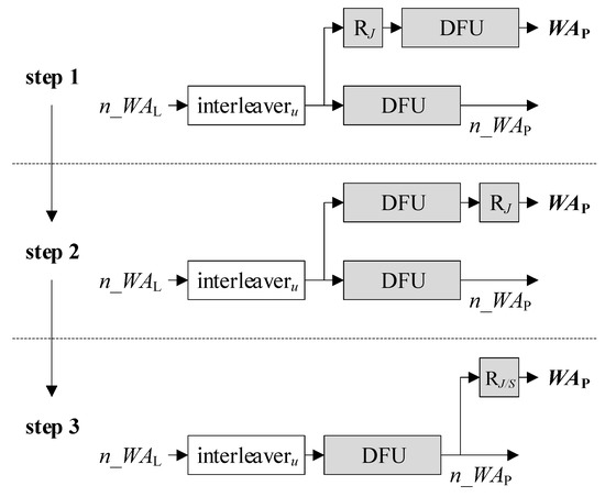
Figure 5.
Step-by-step illustration of removing division-by-S-and-floor unit (DFU) from S-AGU.
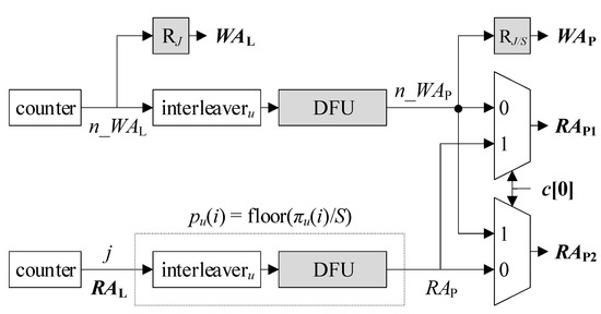
Figure 6.
DFU-reduced S-AGU.
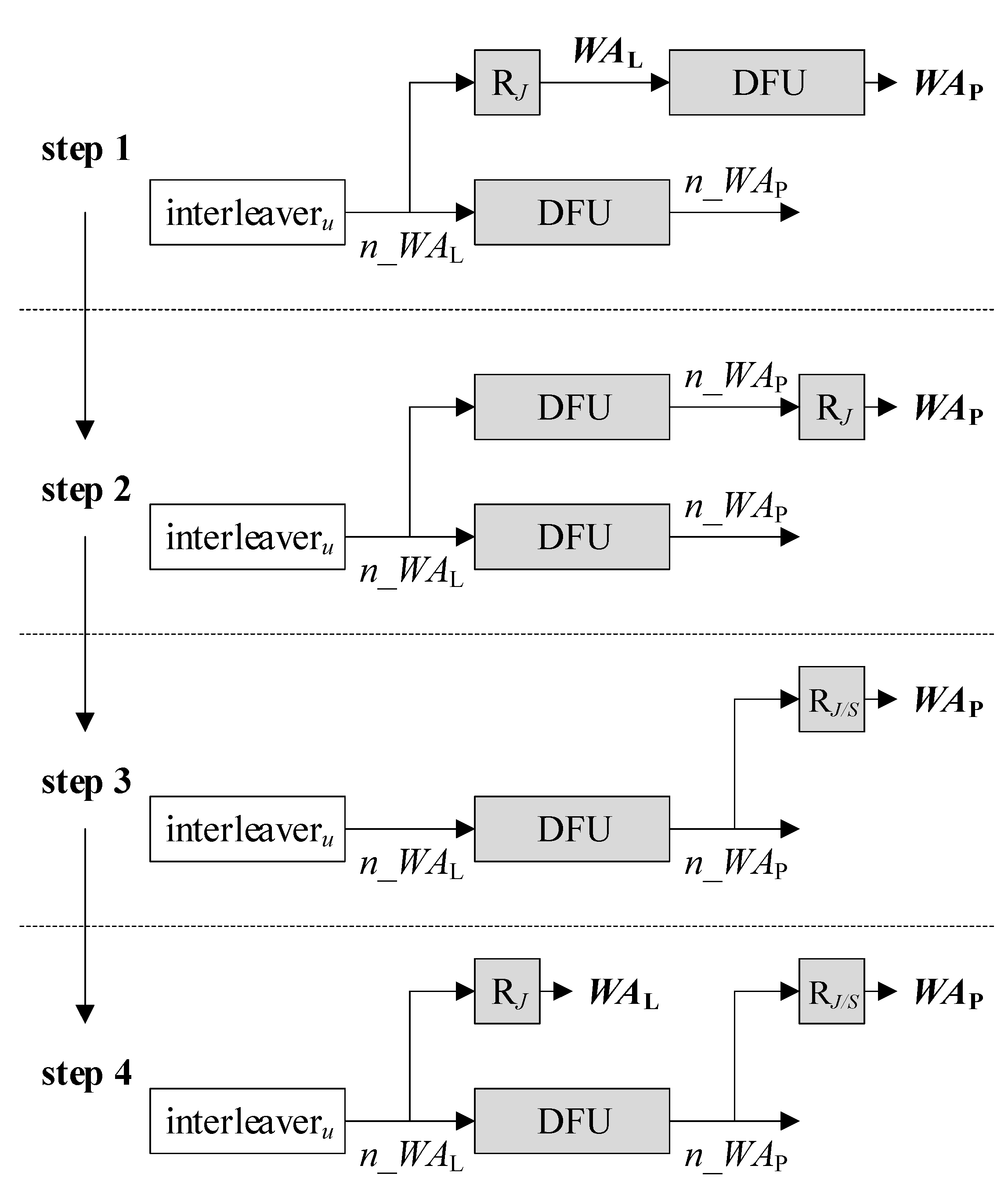
A similar approach can be taken to the I-AGU as well. Step 1 of Figure 7 redraws the top right part of Figure 4. Swapping RJ and the following DFU, we can acquire step 2 of Figure 7. Subsequently, we can share the output of the sole DFU and substitute RJ with RJ/S, as depicted in step 3. However, note that the output of the DFU is now n_WAP, from which WAL cannot be retrieved. To secure the indispensable WAL from n_WAL, we need to add RJ as illustrated in step 4. Unlike the original I-AGU which is of the lowest complexity, the DFU-reduced I-AGU in Figure 8 requires the additional register to hold n_WAP for one cycle. Thus, while one DFU is eliminated, one register is appended. In short, the S-AGU benefits more from the relocation technique than the I-AGU.
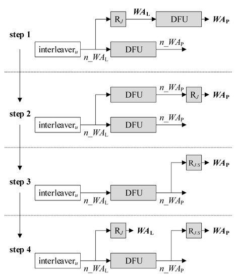
Figure 7.
Step-by-step illustration of removing DFU from I-AGU.
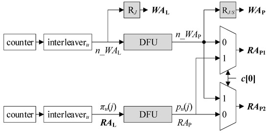
Figure 8.
DFU-reduced I-AGU.
It is worth noting that the complexity of each DFU can be somewhat relieved by confining S to be a power of two, as the division by a power of two can be easily achieved by right-shift operations. In exchange for such a benefit, however, it sacrifices the range of applicability.
5. Evaluation and Discussion
For all kinds of AGU architectures in Figure 3, Figure 4, Figure 6, and Figure 8, Table 2 summarizes the numbers of DFUs and register bits in a U-user detector. The feasibility of single-port ML is also tabulated. Counting all DFUs is apparent, as it is the number of DFUs per AGU multiplied by the number of AGUs in a detector, U. In contrast, register bits should be counted while taking into account the following: the RJ that produces WAL in S-AGUs can be shared among U UPBs, as the SA-based WAL is identical in all UPBs. In case of the original S-AGU, the number of RJ preceding the DFU is U, whereas the number of RJ producing WAL is 1, making the total number of register bits (U + 1)log2J. In the case of the DFU-reduced S-AGU, the numbers of RJ/S and RJ are U and 1, respectively, making the total number of register bits Ulog2(J/S) + log2J. All RJ’s in I-AGUs take different inputs and cannot be shared.

Table 2.
Comparison of AGU architectures.
For the common and practical set of parameters used in Ref. [5,6,7,8], e.g., U = 16, J = 8192, and S = 16, Table 3 enumerates the numbers of DFUs and register bits. The percentages in parentheses are calculated with respect to the original S-AGU. The DFU-reduced S-AGU includes the fewest DFUs and register bits. In particular, it requires 33% fewer DFUs and 29% fewer register bits than the original S-AGU, highlighting the benefits of the proposed relocation. On top of that, it may adopt single-port ML, making it promising in every aspect of hardware complexity.

Table 3.
Numerical example.
In addition to the DFUs and the register bits, the AGUs include other components that contribute to the overall hardware complexity, as follows: algebraic interleavers [9,12]; counters; multiplexers. Besides, identical logics can be synthesized differently as fan-in, fan-out, and gate sizing in circuitry vary. To evaluate more thoroughly by taking such factors into account, the architectures were implemented in a 65 nm CMOS process using a 300 MHz clock and a 1.2 V supply. The corresponding results are summarized in Table 4. Equivalent gates were counted by regarding a two-input nand gate as one. Power consumptions were measured by back-annotating switching activities. The percentages in parentheses are again calculated with respect to the original S-AGU. The original S-AGU and I-AGU are associated with almost the same equivalent gates and powers dissipated. On the contrary, the DFU-reduced S-AGU integrates fewer gates and consumes less power than the DFU-reduced I-AGU, as the latter demands the additional registers in order to obtain WAL. Comparing the original and the DFU-reduced pairs, the DFU-reduced ones dissipate much lower power than their counterparts, owing to the removal of computationally intensive DFUs. In particular, the DFU-reduced S-AGU can be realized with 13% fewer gates, and spends 31% less power than the original S-AGU.

Table 4.
Implementation results.
6. Conclusions
We have analyzed four kinds of AGUs, and have figured out that the proposed DFU-reduced S-AGU is the most outstanding one from the viewpoint of efficient hardware implementation. The results of realization in a 65 nm CMOS have demonstrated that the equivalent gate count and the power dissipation can be mitigated by 13% and 31%, respectively. The reduction in DFUs and register bits has been achieved by exchanging the locations of a DFU and a register, and sharing the output of one DFU rather than employing multiple DFUs. As such a modification is completely transparent, i.e., it does not affect the functionality, it can be readily applied to all the existing multiuser detectors without tailoring the interfacing components therein. Future works include extending the proposed AGU to parallel IDMA architectures [6,8] that adopt different interleaving patterns. Besides this, the algebraic interleavers in AGUs will be investigated for a further reduction of the complexity, as they include several multipliers to be optimized.
Funding
This work was supported in part by the National Research Foundation of Korea grant funded by the Ministry of Science and ICT, Government of South Korea (No. 2020R1G1A1102620), and in part by a research grant of Kongju National University in 2020.
Acknowledgments
EDA tools were supported by the IC Design Education Center, South Korea.
Conflicts of Interest
The author declares no conflict of interest.
References
- Liu, Y.; Elkashlan, M.; Ding, Z.; Nallanathan, A.; Hanzo, L. Nonorthogonal multiple access for 5G and beyond. Proc. IEEE 2017, 105, 2347–2381. [Google Scholar]
- Ping, L.; Liu, L.; Wu, K.; Leung, W.K. Interleave division multiple access. IEEE Trans. Wirel. Commun. 2006, 5, 938–947. [Google Scholar] [CrossRef]
- Zhang, C.; Huang, Y.-H.; Sheikh, F.; Wang, Z. Advanced baseband processing algorithms, circuits, and implementations for 5G communication. IEEE J. Emerg. Sel. Top. Circuits Syst. 2017, 7, 477–490. [Google Scholar] [CrossRef]
- Nguyen, T.T.T.; Lanante, L.; Yoshizawa, S.; Ochi, H. Low latency IDMA with interleaved domain architecture for 5G communications. IEEE J. Emerg. Sel. Top. Circuits Syst. 2017, 7, 582–593. [Google Scholar] [CrossRef]
- Kong, B.Y.; Park, I.-C. A memory-efficient IDMA architecture based on on-the-fly despreading. IEEE J. Solid-State Circuits. 2018, 53, 2677–2688. [Google Scholar] [CrossRef]
- Kong, B.Y.; Park, I.-C. Parallel IDMA architecture based on interleaving with replicated subpatterns. In Proceedings of the IEEE International Conference on Communications, Shanghai, China, 20–24 May 2019; pp. 1–6. [Google Scholar]
- Kong, B.Y.; Park, I.-C. A 120-mW 0.16-ms-latency connectivity-scalable multiuser detector for interleave division multiple access. IEEE Trans. Circuits Syst. II Exp. Briefs 2020, 67, 470–474. [Google Scholar] [CrossRef]
- Kong, B.Y. Improved Parallel-IDMA Architecture with Low-Complexity Elementary Signal Estimators. In Proceedings of the 2020 IEEE International Symposium on Circuits and Systems (ISCAS), Seville, Spain, 10–21 October 2020; pp. 1–4. [Google Scholar]
- Kong, B.Y.; Park, I.-C. Efficient implementation of multiple interleavers in IDMA for 5G. In Proceedings of the 2018 International SoC Design Conference (ISOCC), Daegu, Korea, 12–15 November 2018; pp. 119–120. [Google Scholar]
- Dodd, R.; Schlegel, C.; Gaudet, V. DS-CDMA implementation with iterative multiple access interference cancellation. IEEE Trans. Circuits Syst. I Reg. Pap. 2013, 60, 222–231. [Google Scholar] [CrossRef]
- Yoshizawa, S.; Nozaki, M.; Tanimoto, H. VLSI implementation of an interference canceller using dual-frame processing for OFDM-IDMA systems. IEICE Trans. Fundam. Electron. Commun. Comput. Sci. 2015, 98, 811–819. [Google Scholar] [CrossRef]
- Takeshita, O.Y.; Costello, D.J. New classes of algebraic interleavers for turbo-codes. In Proceedings of the 1998 IEEE International Symposium on Information Theory, Cambridge, MA, USA, 16–21 August 1998; p. 419. [Google Scholar]
Publisher’s Note: MDPI stays neutral with regard to jurisdictional claims in published maps and institutional affiliations. |
© 2020 by the author. Licensee MDPI, Basel, Switzerland. This article is an open access article distributed under the terms and conditions of the Creative Commons Attribution (CC BY) license (http://creativecommons.org/licenses/by/4.0/).

