Article

An Efficient Elliptic-Curve Point Multiplication Architecture for High-Speed Cryptographic Applications

1
Department of Computer Engineering, Umm Al-Qura University, Makkah 21421, Saudi Arabia
2
Science and Technology Unit (STU), Umm Al-Qura University, Makkah 21421, Saudi Arabia
*
Authors to whom correspondence should be addressed.
Electronics 2020, 9(12), 2126; https://doi.org/10.3390/electronics9122126
Submission received: 22 November 2020 / Revised: 1 December 2020 / Accepted: 7 December 2020 / Published: 12 December 2020
(This article belongs to the Section Circuit and Signal Processing)

Abstract

:
This work presents an efficient high-speed hardware architecture for point multiplication (PM) computation of Elliptic-curve cryptography using binary fields over G F ( 2 163 ) and G F ( 2 571 ) . The efficiency is achieved by reducing: (1) the time required for one PM computation and (2) the total number of required clock cycles. The required computational time for one PM computation is reduced by incorporating two modular multipliers (connected in parallel), a serially connected adder after multipliers and two serially connected squarer units (one after the first multiplier and another after the adder). To optimize the total number of required clock cycles, the point addition and point double instructions for PM computation of the Montgomery algorithm are re-structured. The implementation results after place-and-route over G F ( 2 163 ) and G F ( 2 571 ) on a Xilinx Virtex-7 FPGA device reveal that the proposed high-speed architecture is well-suited for the network-related applications, where millions of heterogeneous devices want to connect with the unsecured internet to reach an acceptable performance.

1. Introduction

Information security aims to optimally use a wide variety of cryptographic algorithms in network related applications such as network servers. In this context, two variants of cryptographic algorithms, i.e., symmetric and asymmetric, are commonly involved. Comparatively, the provision of a higher throughput with limited area requirements is the main advantage of symmetric algorithms. However, there are certain drawbacks such as key distribution or key exchange and key management [1,2]. On the other hand, asymmetric algorithms provide authentication and non-repudiating security services effectively without containing the aforementioned drawbacks [3]. Consequently, Elliptic-curve cryptography (ECC) [4,5] and Rivest–Shamir–Adleman (RSA) [6] are more frequently employed asymmetric algorithms.
At the algorithmic level, the security strength of ECC and RSA depends on solving the discrete logarithms and large integer primes, respectively. Both of these asymmetric algorithms are not completely comparable to each other—neither historically nor in terms of performance and age. Additionally, there are several parameters, for example, key length, that eventually affects the security strength and performance of a particular asymmetric cryptographic algorithm [1,3]. Apart from the performance of each particular algorithm, the ECC requires shorter key lengths as compared to RSA [3] for a similar security level. This results in a decrease in power consumption, channel bandwidth requirements and complexity. Therefore, these advantages make ECC an interesting choice for implementations. There are two possibilities to implement ECC: software-based and hardware-based. The hardware-based implementations provide much better results in terms of security improvements by protecting the secret keys and other ECC related parameters [7]. Particularly, the point (or scalar) multiplication (PM) is the most computational intensive operation in ECC [1,3,7]. It further depends on point addition (PA) and point doubling (PD) operations. Each PA and PD operation, in turn, depends on arithmetic operations, i.e., addition, subtraction, multiplication, squaring, and inversion or division. Furthermore, two types of fields (prime G F ( p ) and binary extension G F ( 2 m ) ) are generally involved to implement ECC [3,7]. Each prime or binary field can be adopted either by using the simple affine or projective coordinates [7]. Moreover, the two commonly used options for the point representation are polynomial basis and normal basis.
It has been observed in [3,7,8,9] that the binary field is generally preferred due to efficient hardware implementations of arithmetic operations. Similarly, the projective coordinates are more useful to achieve an efficient high-speed crypto design as compared to affine coordinates, where for each PA and PD operation, an associated inversion operation is essential to compute [9]. Some examples of projective coordinates are standard, homogeneous and Jacobean. A good comparison of these projective coordinates is provided in [9]. In addition to the aforementioned projective coordinates, a relatively new PA formulae for ECC applications is described in [10]. However, the standard projective coordinate system requires fewer instructions for each PA and PD computations, and therefore, has been considered in this article. Furthermore, the normal basis is recommended where frequent squaring operations are involved while the polynomial basis is more convenient where frequent modular multiplications are required [8,9,11,12,13,14,15,16]. Consequently, based on the settings presented above, we consider a standard projective coordinate system to achieve high-speed. Furthermore, for efficient computation of modular multiplications, the polynomial basis is selected.
There are several applications where ECC is practically involved. For example, in mobile security [17], banking applications [18], digital right management systems [19], government communications and so on. Moreover, in many ongoing internet and network applications such as Secure Socket Layer (SSL), Transport Layer Security (TLS), network servers and IPsec protocols, a high-speed computation of arithmetic operations related to ECC is critical [20].

1.1. Existing High-Speed State-of-the-Art Implementations

The most recent high-speed architectures for the computation of PM operation are described in [3,7,11,21,22]. To reduce the required latency for the computation of PM operation of ECC, different techniques have been employed previously: (a) pipelining in the data path of the PM architecture is utilized in [7], (b) pipelining in the utilized modular multipliers is implemented in [3,11,22] and (c) multiple modular arithmetic operators such as adders, multipliers and squarer units are used in the data path of the architecture [3]. A brief overview of various multipliers, used in the aforementioned architectures, is given in [23].
To reduce the clock cycles (latency) and to optimize the PM operation of ECC, the Lopez Dahab based Montgomery algorithm is considered in [3] whereas the implementations are carried out on Virtex-7 over G F ( 2 163 ) . Based on the settings in [3], two different architectures (one for low-latency and another for high-performance) are described. The high-performance architecture employs a single-segmented pipelined full-precision modular multiplier, resulting in 3.18 μ s for one PM computation. The second architecture (low-latency) in [3] utilizes three-segmented pipelined full-precision modular multipliers, resulting in 2.83 μ s for one PM. In addition to the computational time, the clock cycles and FPGA (Field Programmable Gate Array) Slices for high-performance architecture are 1119 and 415, respectively. Similarly, the clock cycles and FPGA resources for low-latency architectures are 450 and 11,657, respectively.
The work in [7] uses two-stage pipeline registers in the data path of the architecture, rather than in the modular multiplier, to optimize the computations for PM operation. By using a digit-parallel modular multiplier with a digit size of 32 bits, the architecture in [7] describes a throughput over area optimized solution, which results in 10.73 μ s for one PM operation over G F ( 2 163 ) on Virtex-7 FPGA. Furthermore, the corresponding values for other design parameters, such as required clock cycles, utilized FPGA Slices and achieved clock frequency, are 3960, 2207 and 369 MHz, respectively.
For high-performance cryptographic applications, another architecture is described in [11], which uses a pipelined bit parallel modular multiplier with an additional accumulator to implement the right-to-left PM algorithm. The performance of the architecture is provided for all NIST (National Institute of Standards and Technology) defined Koblitz curves from G F ( 2 163 ) to G F ( 2 571 ) . Moreover, it requires 2.50 μ s and 18.51 μ s for one PM computation when synthesized for Virtex-5 FPGA over G F ( 2 163 ) and G F ( 2 571 ) field lengths.
Another interesting solution in [21] describes two architectures: one for low-complexity and another for low-latency over G F ( 2 163 ) to G F ( 2 283 ) . The implementation results are provided for different FPGA devices and an ASIC (65nm) technology node. When considering only the results over G F ( 2 163 ) for the recent Virtex-7 FPGA device, the low-complexity architecture employs a single modular multiplier in the data path and results in 3.01 μ s for one PM computation. Moreover, the achieved clock frequency and FPGA Slices for the low-complexity architecture are 264 MHz and 2435, respectively. On the other hand, the low-latency architecture utilizes two modular multipliers in the data path, which results in 1.50 μ s for the computation of one PM operation. Furthermore, the reported clock frequency and FPGA resources for the low-latency architecture are 214 MHz and 5753, respectively.
Finally, the architecture in [22] performs PM operation using the Montgomery ladder algorithm. To speed up the PM operation of ECC, the authors in [22] have employed one digit-serial modular multiplier in the data path and achieves one PM in 3.97 μ s over G F ( 2 163 ) on Virtex-7 FPGA device. The achieved clock frequency and utilized FPGA Slices are 437 MHz and 5575, respectively.

1.2. Limitations in the Existing Solutions

Section 1.1 shows that various architectural styles have been previously proposed with different types of multipliers to speed-up the PM computation process. The aforementioned techniques ultimately reduce the required number of clock cycles and improve the operational clock frequency of the PM architecture. However, there are numerous emerging high-speed applications such as mobile security [17], banking applications [18], digital right management systems [19], and network-related applications (SSL/TLS, network servers, and IPsec protocols) [20], which demand further improvements in the overall throughput of PM computation process. In other words, we believe that the speed or throughput of the PM operation can further be improved by employing multiple arithmetic operators in different design places of the data path.

1.3. Our Contributions

The contributions of this work are provided as:
  • An efficient high-speed hardware architecture for the PM computation of ECC using NIST defined binary fields over G F ( 2 163 ) and G F ( 2 571 ) are presented. The G F ( 2 163 ) field is selected as it allows a richer comparison to the state-of-the-art solutions while the G F ( 2 571 ) field is employed to evaluate the performance of proposed high-speed architecture for higher key lengths.
  • To reduce the computational time for a single PM computation, we incorporate two modular multipliers (connected in parallel), two serially connected squarer units (one after the first multiplier and another after the adder) and a single adder unit (serially connected after multipliers) in the data path of the proposed high-speed PM architecture. The utilization factor for each parallel-connected multiplier is 83% in the loop iteration step of the PM algorithm, as the parallel-connected multipliers are fully utilized in five clock cycles when the total required cycles are six (details are given in Section 3).
  • To reduce clock cycles, we provide an efficient scheduling of PA and PD instructions for PM computation of the Montgomery algorithm. It reduces 57% of clock cycles as compared to PA and PD instructions in the native Montgomery PM algorithm. Consequently, the reduction in computational time and clock cycles ultimately improves the overall speed.
  • Finally, to speed up the control functionalities, a finite-state-machine (FSM) based dedicated control unit is used.
The implementation results after place-and-route over G F ( 2 163 ) and G F ( 2 571 ) on a Virtex-7 FPGA device reveal that the proposed high-speed architecture is an appropriate solution for the network-related applications, i.e., servers, where millions of heterogeneous devices want to connect with the unsecured internet, to reach an acceptable performance. The proposed architecture over G F ( 2 163 ) and G F ( 2 571 ) utilizes lower hardware resources as compared to the most recent state-of-the-art high-speed architectures, described in [3,7,8,11,21]. Moreover, our architecture on Virtex-7 FPGA device requires 64% lower computational time for one PM computation (latency), as compared to the architectures presented in [7,8] over G F ( 2 163 ) . For binary field sizes over 163 and 571, the proposed architecture provides a comparable latency for one PM computation, as compared to the solutions described in [3,11,21]. Consequently, the high-speed architecture in this article is best suited for emerging high-speed applications, as it provides a comparable latency while utilizing much lower hardware resources as compared to the state-of-the-art.
The remainder of this paper is structured as follows: In Section 2, the theoretical background related to the computation of Montgomery PM on ECC over G F ( 2 m ) is presented. Parallelization of PA and PD operations are described in Section 3. The proposed high-speed architecture for PM computation of ECC is discussed in Section 4. Section 5 presents the implementation results and provides a comparison in terms of various performance attributes. Finally, Section 6 concludes the paper.

2. Background

An elliptic-curve over binary, i.e., G F ( 2 m ) field, for Lopez Dahab projective form is defined as a set of points P(X:Y:Z), satisfying the following equation [9]:
E : Y 2 + X Y Z = X 3 Z + a X 2 Z 2 + b Z 4
In Equation (1), the variables X, Y and Z are the Lopez Dahab projective elements of point P(X:Y:Z) where Z 0 , a and b are the curve constants, with b 0 . If PM contains a base point P and a large integer k of the size of the underlying field, then PM is the addition of k copies of point P, i.e., Q = k × ( P + P + + P ) , where Q is a new point on the defined elliptic-curve. In order to compute the PM operation in ECC, we have used the Montgomery algorithm originally described in [24] and shown as Algorithm 1 in this article.
In order to implement Algorithm 1 for PM, it requires a scalar multiplier k along with the initial point P with its coordinates (xp, yp) as an input and produces (xq, yq) coordinates of the final point Q as an output. A description of these steps (Step-1 to Step-3) is given in the following:
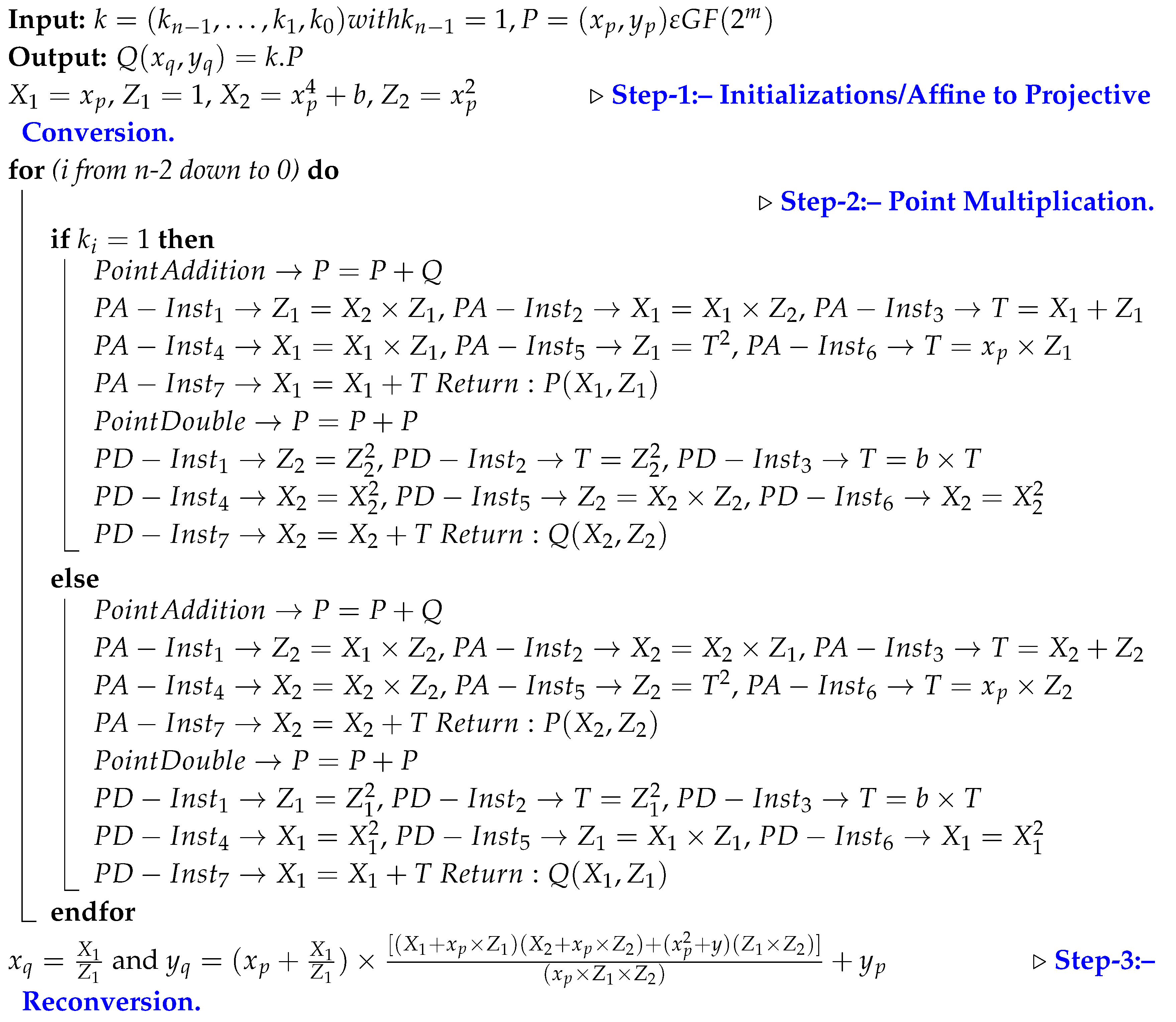
  • The Initialization step (Step-1 in Algorithm 1) ensures the conversions from affine to projective (Lopez Dahab) coordinates.
  • The Point Multiplication step (Step-2 in Algorithm 1) provides some mathematical instructions related to PA ( P = P + Q ) and PD ( P = 2 P ) computations, based on the inspected value of scalar multiplier (ki). As shown in Algorithm 1, the point multiplication step is operated in a loop-fashion. In order to execute this loop in the hardware, i represents the integer value that is responsible for counting the number of points on the defined elliptic curve while n determines the implemented field size (163 or 571 in this work). Once the inspected key bit (i.e., k i ) becomes 1 then the instructions for PA and PD of “if” part of the Algorithm 1 are executed, otherwise the instructions from “else” part are computed.
  • Finally, the Reconversion step (Step-3 in Algorithm 1) provides the instructions related to projective (Lopez Dahab) to affine conversions, including the costly inversion operation.
Algorithm 1: Montgomery point multiplication algorithm [24]
Electronics 09 02126 i001

3. Proposed Instructions Parallelization of Point Addition and Point Doubling Operations

As shown in Algorithm 1, the PA and PD operations require a total of 14 instructions (either the inspected key bit ki is 0 or 1) such that 7 instructions are employed for each PA (PA-Inst1 to PA-Inst7) and PD (PD-Inst1 to PD-Inst7) operations. Furthermore, out of these 14 instructions, 6 instructions are utilized for modular multiplication, 5 instructions are dedicated for modular squaring and the remaining 3 instructions are used for the modular addition operation. Now, for the PM computation, there are two possibilities (cases) to implement these instructions. The first possibility is to use a single modular adder, a multiplier and a squarer unit, as implemented in [7]. It requires 14 clock cycles for each PA and PD computation. The second possibility is the utilization of multiple arithmetic operators to accelerate the performance of the PM step in Algorithm 1, as described in [3,22]. Comparatively, the former (possibility 1) is preferable for all those applications where the hardware area is relatively more important such as in wireless constrained applications while the latter (possibility 2) is more convenient in those scenarios where the speed/throughput is critical, such as, in network-related applications (servers).
Throughput is the ratio of required clock cycles to clock frequency. Therefore, to reduce the required number of clock cycles for PM computation, we have re-structured the PA and PD instructions of Algorithm 1 in Algorithm 2 using two modular multipliers (termed as, MULT−1 and MULT−2), two modular squarer units (named as, SQR−1 and SQR−2) and an adder unit. (This section describes only the proposed instructions parallelization for PA and PD computations without showing the corresponding architecture. We have described the complete architecture using the proposed instructions parallelization in Section 4. However, in this section, it is important to report that the used modular multipliers, i.e., MULT−1 and MULT−2 are connected in parallel. The first modular squarer unit, i.e., SQR−1, is connected serially after the adder unit while another squarer unit, i.e., SQR−2, is connected serially after MULT−1. The adder unit is connected after multipliers (MULT−1 and MULT−2) using routing multiplexers.) The two modular multiplier units are connected in parallel. The serially connected squarer units, one after the multiplier and another after the adder unit are used to perform: (1) Quad power, i.e., A 4 , of a polynomial A (required for inversion computation), and (2) Squaring after addition, i.e., ( A + B ) 2 , of two polynomials A and B. It is important to mention that our architecture is an optimal solution for the proposed parallelization of instructions, as shown in Figure 1. However, the performance of our architecture could be further improved by increasing the number of arithmetic units (multipliers, squarer’s, and adders) in the data path with different scheduling/parallelization schemes/approaches for PA and PD instructions. Consequently, the proposed parallelization scheme for the computation of PA and PD instructions of Algorithm 2 is illustrated in Figure 1.
Algorithm 2: Proposed instructions parallelization for PM computation of Montgomery algorithm using two modular multipliers, two squarers and an adder unit
Electronics 09 02126 i002

3.1. Instructions Parallelization for Point Addition

In order to compute Z1 for PA computation in Algorithm 2, we have combined the instructions, PA−Inst1, PA−Inst2, PA−Inst3, and PA−Inst5 of Algorithm 1, resulting Z1 = ((X2× Z1) + (X1× Z2)) 2 . Using a single adder, a multiplier and a squarer unit, four clock cycles are required to compute these four instructions. However, using two modular multipliers, two squarer units and an adder unit (as connected in this work) requires only one clock cycle (presented as CC−1 in Figure 1) to compute Z1 = ((X2× Z1) + (X1× Z2)) 2 . The remaining three instructions of PA computation in Algorithm 1, i.e., PA−Inst4, PA−Inst6, and PA−Inst7, can be combined to compute X1 = (X1× Z1) + (xp× Z1), as shown in Algorithm 2. Three clock cycles are required for the computation of these three instructions using a single adder, a multiplier, and a squarer unit while using two modular multipliers, two squarer units and an adder unit (as connected in this work), only one clock cycle (shown as CC−2 in Figure 1) is required.

3.2. Instructions Parallelization for Point Doubling

To compute Z2 for the computation of PD, we have combined PD−Inst1, PD−Inst4, and PD−Inst5, of Algorithm 1, resulting in Z2 = (Z2) 2 × (X2) 2 , as shown in Algorithm 2. Considering a single adder, a multiplier and a squarer unit, three clock cycles are required to compute these three instructions. Using two modular multipliers, two squarer units and an adder unit (as connected in this work), two clock cycles (shown as CC−3 and CC−4 in Figure 1) are required to compute these instructions, i.e., computation of (X2) 2 and (Z2) 2 using MULT−1 and MULT−2 in one clock cycle (CC−3) and the product of these instructions, i.e., (X2) 2 ×(Z2) 2 using the MULT−1 in the next clock cycle (CC−4), as shown in Figure 1. The remaining four instructions for PD computation of Algorithm 1, i.e., PD−Inst2, PD−Inst3, PD−Inst6, and PD−Inst7 are combined to compute X2 = ((Z2 4 × b) + X2 4 ), as shown in Algorithm 2. Using two modular multipliers, two squarer units and an adder unit (as connected in this work), these instructions can be computed in three clock cycles, i.e., computation of Z2 4 using MULT−2 in CC−4, computation of X2 4 (using MULT−1 and SQR−2) and Z2 4 ×b (using MULT−2) in clock cycle CC−5. Finally, the sum of Z2 4 × b and X2 4 is computed in clock cycle CC−6, as shown in Figure 1.

3.3. Overall Decrease in Total Number of Clock Cycles

The proposed parallelization scheme for the computation of PA and PD instructions of Algorithm 2 requires only sic clock cycles (shown as CC−1 to CC−6 in Figure 1). The first two clock cycles (shown as CC−1 and CC−2) are required to compute PA instructions of Algorithm 2 while the remaining four clock cycles (shown as CC−3 to CC−6) are required to compute PD instructions of Algorithm 2. In other words, the required number of clock cycles are reduced from 14 to 6 (a total decrease of 8 clock cycles). Consequently, the proposed parallelization scheme for the computation of PA and PD instructions of Algorithm 2 results in 57% (the ratio of 8 to 14) decrease in the required number of clock cycles as compared to PA and PD instructions of Algorithm 1. Furthermore, the parallel-connected multipliers are used only in clock cycles CC−1 to CC−5 and not in the clock cycle CC−6, as shown in Figure 1. Therefore, the utilization factor for each parallel-connected multiplier is 83% (the ratio of five to six) in the loop iteration step of the selected Montgomery PM algorithm.

4. Proposed High-Speed Elliptic-Curve Point Multiplication Architecture

The proposed high-speed elliptic-curve PM architecture consists of a memory unit (an array of registers), a data path unit and a Finite State Machine based dedicated control unit, as shown in Figure 2. (The initial curve parameters, i.e., Basepoint_xp, Basepoint_yp, and constant_b for the proposed PM architecture are selected from NIST recommended document [25]). The control signals, generated by the control unit, for the corresponding read/write operations over the memory unit and for the routing multiplexers in the data path are shown with the red color lines in Figure 2. There are 12 control signals, i.e., C1 to C12, generated by the control unit. The C1 to C5 are used for the memory related operations (read/write) while C6 to C11 are utilized for various routing purposes in the data path. The control signal C12 is used to drive the output of the data path to the memory unit for the writeback of the intermediate/final result.

4.1. Memory Unit

The memory unit of proposed architecture contains an 8 × m size of register array. The numerical term (i.e., 8) determines the total number of memory addresses in the register array while the value of m shows the number of bits stored at each address. The objective of this unit is to keep the intermediate results in addresses X 1 , X 2 , Z 1 , Z 2 , T 1 , T 2 , T 3 , and T 4 during the implementation of Algorithm 2. As shown in Figure 2, it includes four multiplexers of 8 × 1 size to read the required operands from the memory unit to the data path. Moreover, it contains a de-multiplexer of size 1 × 8 to modify the contents of each particular memory address, using the corresponding ALU_OUT signal. Finally, a single clock cycle is required to perform each read/write operation using the aforementioned multiplexers and a de-multiplexer, respectively.

4.2. Data Path

The overall structure of the data path is described in Section 4.2.1. Subsequently, the implementation of each modular operator in the data path is discussed in Section 4.2.2.

4.2.1. Structure of the Data Path

As introduced in Section 3 of this paper, the data path of the proposed architecture contains two modular multipliers (MULT−1 and MULT−2), two modular squarer units (SQR−1 and SQR−2) and an adder unit, as shown in Figure 2. In addition to the aforementioned arithmetic operators, seven multiplexers at various places of the data path are used for routing purposes. Out of these seven multiplexers, the size of three multiplexers (MUX_E, MUX_F and MUX_G) is 4 × 1 . Similarly, the size of multiplexers (MUX_H, MUX_I and MUX_J) is 2 × 1 . Finally, the size of multiplexer (MUX_K) is 5 × 1 .
The employed modular multipliers, i.e., MULT−1, and MULT−2 are connected in parallel. To operate these multipliers in parallel, various multiplexers (MUX_E, MUX_F, MUX_G, MUX_H, MUX_I and MUX_J) are used. The input to the multiplexers, i.e., MUX_E, MUX_F and MUX_G are curve constants B a s e p o i n t x p , B a s e p o i n t y p and C o n s t a n t b along with an operand from the memory unit, as shown in Figure 2. The corresponding outputs of multiplexers MUX_E, MUX_F and MUX_G are the first inputs to MUX_J, MUX_H and MULT−2, respectively. The second inputs to the MUX_J and MUX_H are the outputs of MULT−1 and MULT−2, respectively. Similarly, the inputs to the MUX_I are from the output of MULT−2 and an operand from the memory unit. The outputs of MUX_J and MUX_I are inputs to the MULT−1. The output of MUX_H is the input to MULT−2, as a second operand. Consequently, the placement of routing multiplexers at multipliers input, shown in Figure 2, significantly reduces the required number of clock cycles to accelerate the Step−2 (PM) of Algorithm 2.
The output of MULT−1 is an input to the squarer, i.e., SQR−2, to compute the squaring after modular multiplication. The placement of a squarer after the multiplier facilitates the reduction of clock cycles required for the Step−3 of Algorithm 2 (as it includes the modular inversion operation that requires higher clock cycles for computation). Moreover, this placement allows us to compute A(x) 4 in one clock cycle when A(x) is the input polynomial (it computes by providing similar inputs, i.e., A(x), to MULT−1 and then the squaring using SQR−2 after multiplication computation).
As shown in Step−1, 2, and 3 of Algorithm 2, the adder unit is required: (1) for the addition of two input polynomials A(x)+B(x), (2) after the multiplication of two input polynomials ((A(x) × B(x))+C(x)) and (3) before squaring of two input polynomials ((A(x) × B(x))+C(x)) 2 . However, the placement of the adder unit in the proposed architecture, shown in Figure 2, allows us to perform the aforementioned computations in one clock cycle. Finally, a MUX_K is used in the proposed high-speed PM architecture to writeback the intermediate/final results of Algorithm 2 on the memory unit.

4.2.2. Implementation of Modular Operators

The details of modular operators required for the implementation of Algorithm 2 is provided as:
  • Adder: The polynomial addition is implemented using bitwise exclusive−OR (XOR) gates as described in [3,7,8,9,11,21,22].
  • Multipliers: To perform multiplication of two m bit input polynomials, i.e., A(x) × B(x) over G F ( 2 m ) , a Parallel-Least-Significant-Digit (P-LSD) multiplier with a digit size of 41 bits is employed inside the used MULT−1 and MULT−2 multipliers (shown in Figure 2). The digits with d = 41 bits of input polynomial B ( x ) is created ( B 1 B 4 ) by generating the partial products. Parallel multiplication of each created digit ( B 1 B 4 ) is performed with the input polynomial, i.e., A ( x ) . For example, to compute FF multiplication over G F ( 2 163 ) , a total of four digits are required. Out of these four digits, three digits ( B 1 B 3 ) are with the size of 41 bits while the last digit ( B 4 ) is with 40 bit size. The parallel multiplication of each B 1 B 4 digit with an m bit polynomial A(x), results d + m 1 bits. After multiplication of each d bit digit with an m bit polynomial, the resultant polynomial, i.e., D ( x ) = 2 × m 1 bit, is created using shift and add operations over polynomials size of d + m 1 bits. Similarly, to compute FF multiplication over G F ( 2 571 ) , a total of fourteen digits ( B 1 B 14 ) are required. The first thirteen digits ( B 1 B 13 ) are with 41 bit size while the remaining digit ( B 14 ) is with 38 bit size.
  • Squarer Units: The used squarer units, SQR−1 and SQR−2 in Figure 2, for polynomial squaring are implemented by incorporating a bit 0 after each input data bit, as described in [9]. It takes an m bit polynomial as input and produces a resultant polynomial of size 2 × m 1 bits.
  • Modular reduction (not shown in Figure 2): The multiplication of two m bit polynomials, i.e., A ( x ) × B ( x ) and squaring over an m bit polynomial, i.e., A(x) 2 , produces a resultant polynomial of degree 2 × m 1 bits. Therefore, after each FF multiplication and a squaring operation, a modular reduction is essential to perform. However, we have implemented NIST reduction algorithms over G F ( 2 163 ) and G F ( 2 571 ) fields, respectively (as described in Algorithm 2.41 and 2.45 in reference [9]).
  • Polynomial inversion (not shown in Figure 2). The polynomial inversion over G F ( 2 m ) is implemented by using the Itoh−Tsujii algorithm [26]. It requires repeated squares followed with multiplications for inversion computations. For example, for G F ( 2 163 ) , 162 squares followed with 9 multiplications are needed. Similarly, 570 squares followed with 11 multiplications are required to perform inversion over G F ( 2 571 ) . Subsequently, there are two possibilities to implement repeated squares in the Itoh−Tsujii algorithm. In the first case, each square is required to compute in one clock cycle (termed as, square version of Itoh-Tsujii). In the second case, two repeated squares are performed in one clock cycle (named as, quad-block version of Itoh-Tsujii). Comparatively, the latter is more convenient to reduce the total number of clock cycles in high-speed elliptic-curve computations. Consequently, we have used the quad-block version of the Itoh–Tsujii algorithm for polynomial inversion computation using serially connected MULT−1 and SQR−2, as shown in Figure 2.

4.3. Control Unit

An FSM based dedicated control unit is designed to generate control functionalities. To implement the Montgomery algorithm for ECC PM computation, as shown in Algorithm 2, the dedicated FSM contains a total of 42 and 44 states over G F ( 2 163 ) and G F ( 2 571 ) , respectively. Due to space limitations, only the sequence of control unit states along with their control signals for G F ( 2 571 ) are shown in Figure 3.
The details of FSM states are given as:
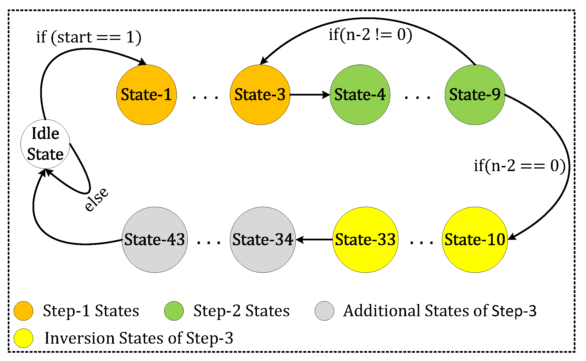
  • Idle state: The state-0 is an idle state. The architecture begins execution based on the value of start signal, as illustrated in Figure 3.
  • Step-1 of Algorithm 2: State-1 to State-3 are responsible for generating control signals for the initialization (affine to projective conversion) step of Algorithm 2, as shown in Figure 3.
  • Step-2 of Algorithm 2: State-4 to State-9 generate control signals for the execution of the PM step (PA and PD instructions). Moreover, each state is responsible for checking the inspected key bit k i (this information is not provided in Figure 3). Once the value of k i becomes 1, the corresponding PA and PD instructions from the if part of Algorithm 2 are executed. Otherwise, the instructions from else part of Algorithm 2 are computed. The State-9 is also responsible for checking the value on n to count the number of points on the defined elliptic curve. Once the value of n 2 becomes 0 (the implemented field size—163 or 571—is the initial value to n) then the next-state will be State-10 otherwise the next-state will be State-3. These states (State-3 to State-9) continue their execution until the value of n 2 becomes 0.
  • Step-3 of Algorithm 2: For G F ( 2 163 ) , State-10 to State-41 (State-10 to State-31 are for inversions and the remaining states are required for the computation of additional instructions in Algorithm 2) are required to perform Lopez Dahab to affine conversions. Similarly, for G F ( 2 571 ) this figure increases to 43 meaning that State-10 to State-33 are required for inversion computation and the additional states (State-34 to State-43) are required to execute remaining instructions in the projective to affine conversions of Algorithm 2.
The total number of required clock cycles, for the proposed high-speed architecture, are calculated by using Equation (3). Three clock cycles are required to perform Step-1 of Algorithm 2. For the computation of Step-2, 6 × ( m 1 ) clock cycles are required. Finally, Step-3 includes clock cycles for the inversion operation (92 for G F ( 2 163 ) and 297 for G F ( 2 571 ) ). Furthermore, it requires additional 12 clock cycles for the computation of remaining operations of Step-3 in Algorithm 2.
Total   clock   cycles = 3 S t e p 1 + 6 × ( m 1 ) S t e p 2 + i n v e r s i o n + 12 S t e p 3

5. Implementation Results and Comparisons

This section first provides the implementation results of the proposed architecture in Section 5.1. Subsequently, Section 5.2 compares the achieved results with state-of-the-art.

5.1. Implementation Results of the Proposed Architecture over G F ( 2 m ) for m = 163 Bits and 571 Bits

The proposed high-speed architecture over G F ( 2 m ) for m = 163 bits and 571 bits is modeled in Verilog (HDL) using Xilinx ISE 14.5 tool. The implementation results of the proposed architecture over Xilinx Virtex-7 FPGA device for G F ( 2 163 ) and G F ( 2 571 ) are presented in Table 1. Column one of Table 1 provides the field length (m). The area values in terms of FPGA Slices, look-up-tables (LUTs), and flip-flops (FFs) are reported in columns two to four, respectively. Similarly, the timing values in terms of total clock cycles (calculated by using Equation (2)), clock frequency (Freq—in MHz) and latency (in μ s—calculated by using Equation (3)) are provided in columns five to seven, respectively. Finally, the last column of Table 1 shows the number of utilized resources in the proposed data path.
As described earlier, the persistence of this work is to speed-up the PM computation in ECC. In this context, the term latency determines the time required to perform one PM computation and is calculated by using Equation (3).
Latency   ( in   μ s ) = k . P ( in   μ s ) = number   of   clock   cycles clock   frequency   ( in   MHz )
As shown in column two of Table 1, the proposed architecture utilizes 1593 and 5575 FPGA Slices over G F ( 2 163 ) and G F ( 2 571 ) bit key lengths, respectively. Moreover, an operational clock frequency of 293 and 269 MHz is achieved. The time required to perform one PM is 3.68 μ s and 13.87 μ s, respectively.

5.2. Comparison with State-of-the-Art Solutions

The latency and area comparisons with state-of-the-art implementations over G F ( 2 163 ) and G F ( 2 571 ) are provided in Table 2. The first column of Table 2 provides the reference solutions while the number of bits or key length (m) is provided in the second column. The corresponding FPGA device for implementations is shown in column three. The area information in terms of FPGA Slices is presented in column four. Similarly, the timing information in terms of clock cycles, frequency (in MHz), and latency (in μ s) are shown in columns five to seven, respectively. Finally, the last column provides the number of utilized multipliers in the data path to speed-up the PM implementations.

5.2.1. Comparison over Virtex-5

When considering only the hardware resources (FPGA Slices) for comparisons, the proposed architecture utilizes 63% and 78% lower Slices over G F ( 2 163 ) and G F ( 2 571 ) bit key lengths, as compared to the work in [11]. Although the work in [11] requires 45% lower clock cycles, it achieves 12% and 54% lower clock frequency as compared to the proposed work over G F ( 2 163 ) and G F ( 2 571 ) , respectively. This is due to the use of a dedicated power block for inversion computations in [11], while our work is utilizing the resources of multiplier and squarer units for this particular task and no dedicated hardware unit is included in the architecture. It ultimately reduces the hardware resources and critical path in our work, which increases the clock frequency. The use of a dedicated hardware unit in [11] for inversion computation decreases the number of clock cycles.
In addition to the area and clock frequency, the architecture of [11] over G F ( 2 163 ) achieves 36% lower latency as compared to the proposed work. However, over G F ( 2 571 ) , the proposed architecture attains 15% lower latency as compared to the solution described in [11]. For a longer key length (such as of G F ( 2 571 ) ), the additional power block in [11] results in a longer critical path delay, which decreases the clock frequency, as shown in Table 2. Therefore, our architecture shows better latency for longer key lengths as compared to [11], while over shorter key lengths, the solution presented in [11] results in better latency as compared to our work.

5.2.2. Comparison over Virtex-7

As shown in the last column of Table 2, the work in [3] provides two different architectures: (1) a low-latency ECC implementation with three modular multipliers (LLECC_3M) and (2) a high-speed pipelined ECC implementation with one modular multiplier (HPECC_1M). When considering the LLECC_3M architecture over G F ( 2 163 ) , the proposed architecture utilizes 87% fewer Slices and achieves 54% higher clock frequency. However, the LLECC_3M architecture requires 60% fewer clock cycles and 24% lower computational time (latency) as compared to our work. The use of one additional multiplier in the data path of LLECC_3M architecture increases the hardware resources and critical path as compared to the proposed work. Moreover, the use of one additional multiplier reduces the clock cycles, which influences the required computational time. Similarly, the HPECC_1M architecture of [3] over G F ( 2 163 ) utilizes 60% more Slices and requires 4% more clock cycles as compared to the proposed work. At the same time, it achieves 17% higher operational clock frequency and takes 14% less computational time. On the other hand, the HPECC_1M architecture over G F ( 2 571 ) utilizes 89%, 2% and 60% more FPGA Slices, clock cycles and latency. Additionally, it achieves 54% less clock frequency. The placement of pipeline registers, in the data path of [3] over G F ( 2 571 ) , does not show a significant improvement in clock frequency. Consequently, the proposed architecture outperforms the work in [3] for higher key lengths (571).
Similar to the work in [3], two different architectures have been described in [21]: (1) a low-complexity architecture with one pipelined modular multiplier in the data path (LC_1M) and (2) a low-latency architecture with two pipelined modular multipliers (LL_2M) in the data path, as shown in the last column of Table 2. When considering the LC_1M architecture over G F ( 2 163 ) , the proposed architecture utilizes 35% fewer Slices and achieves 10% higher clock frequency. However, the LC_1M architecture requires 19% less computational time as it uses a pipelining scheme in the utilized Karatsuba–Offman multiplier (KOM). Similarly, the LL_2M architecture of [21] over G F ( 2 163 ) utilizes 73% more Slices and achieves 27% less clock frequency as compared to our work. At the same time, it requires 60% less computational time. Consequently, the LC_1M and LL_2M cores of [21] over G F ( 2 163 ) increase the hardware resources as they employ pipelining in the used KOM multipliers when compared to our work. In addition to the area, the proposed work also outperforms the pipelined LC_1M and LL_2M cores of [21] over G F ( 2 163 ) in terms of clock frequency.
As compared to the proposed work, the architecture in [7] over G F ( 2 163 ) requires 28%, 73% and 66% more FPGA Slices, clock cycles and computational time, respectively. Only the clock frequency achieved in [7] is 21% higher than this work as it uses the pipelined registers in the data path. Moreover, the scheduling of instructions for PA and PD computations are completely different from [7], which decreases the total number of clock cycles. The decrease in clock cycles ultimately reduces the time required for the one PM computation.
The architecture in [8] over G F ( 2 163 ) uses 8% fewer Slices and attains a 27% higher clock frequency, as compared to the work in this article. However, the work in this article requires 75% fewer clock cycles and a 65% lower computational time, as compared to the architecture in [8]. Moreover, the architecture of [8] over G F ( 2 571 ) utilizes 57%, 74% and 73.6% higher FPGA Slices, clock cycles, and latency, respectively. Additionally, it achieves an 8% lower clock frequency. The use of P-LSD multiplier with a digit size of 41 bits in our work increases the performance in terms of clock cycles and latency as compared to the segmented pipelined most-significant-digit (MSD) multiplier, employed in [8]. Therefore, the use of P-LSD multiplier outperforms the use of the MSD multiplier [8] for higher key length (571) over G F ( 2 m ) . Finally, the architecture in [22] over G F ( 2 163 ) utilizes 72% higher FPGA Slices and requires 8% higher computational time (latency) as compared to our work. However, it achieves a 33% higher clock frequency as it uses a pipelined digit serial multiplier in the data path. At the same time, the use of various squarer units and the additional pipeline registers inside the Itoh–Tsujii inversion block of [22] increases the hardware resources.
To summarize, the proposed high-speed architecture on Virtex-7 FPGA requires 3.68 μ s and 13.87 μ s for one PM computation (latency) over G F ( 2 163 ) and G F ( 2 571 ) , respectively. The corresponding utilized FPGA Slices are 1593 and 5575. There is always a trade-off between hardware resources and computational time (latency). Thus, the proposed hardware architecture over G F ( 2 163 ) and G F ( 2 571 ) utilizes lower FPGA Slices, except the solution shown in [8] for G F ( 2 163 ) , as compared to the most recent state-of-the-art (shown in column four of Table 2). Moreover, the proposed architecture outperforms state-of-the-art solutions in terms of computational time (latency) for higher key lengths (571).

6. Conclusions

This article has presented an efficient high-speed PM architecture over binary fields G F ( 2 163 ) and G F ( 2 571 ) , providing a better performance in terms of computational time on FPGA, while comparing with recent state-of-the-art solutions. To do this, we have reduced the required computational time (latency) of PM computation using two modular multipliers, two squarer units and an adder unit in the data path, which results in a 60%, 74% and 15% decrease in latency over the G F ( 2 571 ) field as compared to [3,8,11]. Similarly, for G F ( 2 163 ) , the proposed architecture requires 66% and 65% lower latency as compared to [7,8]. Moreover, to reduce the total number of clock cycles, we have re-structured the PA and PD instructions for PM computation of the Montgomery algorithm, which results in a 57% decrease in the total number of clock cycles, as compared to the requirements in the native algorithm. The implementation results, captured after place-and-route over G F ( 2 163 ) and G F ( 2 571 ) on Xilinx Virtex-7 FPGA, reveal that the proposed high-speed architecture is well-suited for the high speed network-related applications.

Author Contributions

Conceptualization, M.I. and M.R.; methodology, M.I. and A.S.; validation, M.I. and M.R.; formal analysis, M.I. and A.S; investigation, M.I. and M.R.; resources, M.I. and A.S.; data curation, M.I. and A.S.; writing—original draft preparation, M.I.; writing—review and editing, M.R.; visualization, M.R.; supervision, M.R.; project administration, M.R.; funding acquisition, M.R. All authors have read and agreed to the published version of the manuscript.

Funding

This project is funded by NSTIP (National, Science Technology and Innovative Plan), Saudi Arabia under grant number 14-ELE1049-10.

Acknowledgments

We acknowledge the support of KACST (King Abdul-Aziz City for Science and Technology) and STU (Science and Technology Unit) Makkah.

Conflicts of Interest

The authors declare no conflict of interest.

References

  1. Rashid, M.; Imran, M.; Jafri, A.R.; Al-Somani, T.F. Flexible Architectures for Cryptographic Algorithms—A Systematic Literature Review. J. Circuits Syst. Comput. 2019, 28, 1992002. [Google Scholar] [CrossRef] [Green Version]
  2. Rashid, M.; Imran, M.; Jafri, A.R.; Al-Somani, T.F. Comparative analysis of flexible cryptographic implementations. In Proceedings of the 11th International Symposium on Reconfigurable Communication-Centric Systems-on-Chip, Tallinn, Estonia, 27–29 June 2016; pp. 1–6. [Google Scholar]
  3. Khan, Z.U.A.; Benaissa, M. High-Speed and Low-Latency ECC Processor Implementation Over GF(2m) on FPGA. IEEE Trans. Very Large Scale Integr. Syst. 2017, 25, 165–176. [Google Scholar] [CrossRef] [Green Version]
  4. Koblitz, N. Elliptic curve cryptosystems. Math. Comput. 1987, 48, 203–209. [Google Scholar] [CrossRef]
  5. Miller, V. Use of elliptic curves in cryptography. In Advances in Cryptology— CRYPTO ’85 Proceedings; 218 of the Series Lecture Notes in Computer Science (LNCS); Williams, H.C., Ed.; Springer: Berlin/Heidelberg, Germany, 1986; pp. 417–426. [Google Scholar]
  6. Rivest, R.L.; Shamir, A.; Adleman, L. A method for obtaining digital signatures and public-key cryptosystems. Commun. ACM 1978, 21, 120–126. [Google Scholar] [CrossRef]
  7. Imran, M.; Rashid, M.; Jafri, A.R.; Kashif, M. Throughput/area optimized pipelined architecture for elliptic curve crypto processor. IET Comput. Digit. Tech. 2019, 13, 361–368. [Google Scholar] [CrossRef] [Green Version]
  8. Khan, Z.; Benaissa, M. Throughput/area-efficient ECC processor using Montgomery point multiplication on FPGA. IEEE Trans. Circuits Syst. II 2015, 62, 1078–1082. [Google Scholar] [CrossRef]
  9. Hankerson, D.; Menezes, A.; Vanstone, S. Finite Field Arithmetic. In Guide to Elliptic Curve Cryptography; Publishing House: New York, NY, USA, 2004; pp. 32–58. [Google Scholar]
  10. Méloni, N. New Point Addition Formulae for ECC Applications. In Proceedings of the WAIFI: Workshop on the Arithmetic of Finite Fields, Madrid, Spain, 21–22 June 2007; pp. 189–201. [Google Scholar]
  11. Li, L.; Li, S. High-performance pipelined architecture of point multiplication on koblitz curves. IEEE Trans. Circuits Syst. II Express Briefs 2018, 65, 1723–1727. [Google Scholar] [CrossRef]
  12. Rashid, M.; Imran, M.; Jafri, A.R.; Mehmood, Z. A 4-Stage Pipelined Architecture for Point Multiplication of Binary Huff Curves. J. Circuits Syst. Comput. 2020, 29, 2050179. [Google Scholar] [CrossRef]
  13. Imran, M.; Rashid, M.; Jafri, A.R.; Islam, M.N. ACryp-Proc: Flexible Asymmetric Crypto Processor for Point Multiplication. IEEE Access 2018, 6, 22778–22793. [Google Scholar] [CrossRef]
  14. Jafri, A.R.; Islam, M.N.; Imran, M.; Rashid, M. Towards an Optimized Architecture for Unified Binary Huff Curves. J. Circuits Syst. Comput. 2017, 26, 1750178. [Google Scholar] [CrossRef]
  15. Hu, X.; Zheng, X.; Zhang, S.; Cai, S.; Xiong, X. A low hardware consumption elliptic curve cryptographic architecture over GF(p) in embedded application. Electronics 2018, 7, 104. [Google Scholar] [CrossRef] [Green Version]
  16. Javeed, K.; Wang, X.; Scott, M. High performance hardware support for elliptic curve cryptography over general prime field. Microprcessors Microsyst. 2017, 51, 331–342. [Google Scholar] [CrossRef]
  17. Hamlin, A. Overview of Elliptic Curve Cryptography on Mobile Devices. Available online: https://pdfs.semanticscholar.org/e6dc/f250c18d37dfd380efe01f13ee4b24cef702.pdf (accessed on 11 November 2020).
  18. Mohammadi, S.; Abedi, S. ECC-Based biometric signature: A new approach in electronic banking security. In Proceedings of the International symposium on Electronic Commerce and Security, Guangzhou, China, 3–5 August 2008; pp. 763–766. [Google Scholar]
  19. Lee, C.; Li, C.; Chen, Z.; Chen, S.; Lai, Y. A novel authentication scheme for anonymity and digital rights management based on elliptic curve cryptography. Int. J. Electron. Secur. Digit. Forensics 2019, 11, 96–117. [Google Scholar] [CrossRef]
  20. Intel-White Paper. Understanding the SSL/TLS Adoption of Elliptic Curve Cryptography (ECC). Commun. Serv. Provid. Netw. Secur. Available online: https://builders.intel.com/docs/networkbuilders/understanding-the-ssl-tls-adoption-of-elliptic-curve-cryptography.pdf (accessed on 4 November 2020).
  21. Salarifard, R.; Bayat-Sarmadi, S.; Mosanaei-Boorani, H. A low-latency and low-complexity point-multiplication in ECC. IEEE Trans. Circuits Syst. I Regul. Pap. 2018, 65, 2869–2877. [Google Scholar] [CrossRef]
  22. Rashidi, B.; Masoud Sayedi, S.; Rezaeian Farashahi, R. High-speed hardware architecture of scalar multiplication for binary elliptic curve cryptosystems. Microelectron. J. 2016, 52, 49–65. [Google Scholar] [CrossRef]
  23. Imran, M.; Rashid, M. Architectural review of polynomial bases finite field multipliers over GF(2m). In Proceedings of the 2017 International Conference on Communication, Computing and Digital Systems (C-CODE), Islamabad, Pakistan, 8–9 March 2017; pp. 331–336. [Google Scholar]
  24. Montgomery, P.L. Speeding the pollard and elliptic curve methods of factorization. Math. Comput. 1987, 48, 243–264. [Google Scholar] [CrossRef]
  25. Federal Information Processing Standards Publication (FIPS PUB 186-4). Digital Signature Standard (DSS). Available online: https://nvlpubs.nist.gov/nistpubs/FIPS/NIST.FIPS.186-4.pdf (accessed on 9 November 2020).
  26. Itoh, T.; Tsujii, S. A fast algorithm for computing multiplicative inverses in GF(2m) using normal bases. Inf. Comput. 1988, 78, 171–177. [Google Scholar] [CrossRef] [Green Version]
Figure 1. Proposed parallelization scheme for the computation of point addition (PA) and point doubling (PD) instructions.
Electronics 09 02126 g001
Figure 2. Proposed high-speed elliptic-curve point multiplication architecture.
Electronics 09 02126 g002
Figure 3. Control unit of the proposed architecture for G F ( 2 571 ) .
Electronics 09 02126 g003
Table 1. Implementation results of the proposed high-speed elliptic-curve PM architecture after post-place-and-route over G F ( 2 m ) for m = 163 and 571 on a Xilinx XC7VX690T device.
mSlicesLUTsFFsClock CyclesFrequency (in MHz)Latency (in μ s)# of Used Resources
B-16315935097132810792933.681 ADD, 2 SQR and 2 MULT
B-571557517,8394596373226913.87
ADD. adder, SQR. squarer, MULT. Least-significant digit-parallel multiplier with digit size of 41 bits.
Table 2. Comparison with state-of-the-art over G F ( 2 163 ) and G F ( 2 571 ) on Xilinx FPGA devices.
ReferencemDeviceSlicesClock CyclesFrequency (in MHz)Latency (in μ s)# of Used Multipliers
[3]B-163Virtex-711,6574501592.83LLECC_3M (three 163 bit mul)
[3]B-163Virtex-7415011193523.18HPECC_1M (one 163 bit mul)
[7]B-163Virtex-72207396036910.73one digit-parallel
[8]B-163Virtex-71476416839710.511 digit-serial
[11]K-163Virtex-536706142452.50-
[21]B-163Virtex-72435-2643.01LC_1M
[21]B-163Virtex-75753-2141.50LL_2M
[22]B-163Virtex-75575-4373.971 digit-serial
[3]B-571Virtex-750,336378311134.05HPECC_1M (one 571 bit mul)
[8]B-571Virtex-712,96514,39625057.611 digit-serial
[11]K-571Virtex-520,291205611118.51-
This workB-163Virtex-5138410792763.90two digit-parallel
B-163Virtex-7159310792933.68
B-571Virtex-54542373223715.74
B-571Virtex-75575373226913.87
LLECC_3M: low-latency ECC architecture with three modular FF multipliers in the data path; HPECC_1M: high-speed ECC architecture with one modular FF multiplier in the data path; LC_1M: low-complexity ECC architecture with one modular FF multiplier in the data path; LL_2M: low-latency ECC architecture with two modular FF multipliers in the data path.
Publisher’s Note: MDPI stays neutral with regard to jurisdictional claims in published maps and institutional affiliations.

